JP7344968B2 - センサ装置 - Google Patents
センサ装置 Download PDFInfo
- Publication number
- JP7344968B2 JP7344968B2 JP2021541871A JP2021541871A JP7344968B2 JP 7344968 B2 JP7344968 B2 JP 7344968B2 JP 2021541871 A JP2021541871 A JP 2021541871A JP 2021541871 A JP2021541871 A JP 2021541871A JP 7344968 B2 JP7344968 B2 JP 7344968B2
- Authority
- JP
- Japan
- Prior art keywords
- sensor
- electrode
- electrodes
- shield
- sensor device
- Prior art date
- Legal status (The legal status is an assumption and is not a legal conclusion. Google has not performed a legal analysis and makes no representation as to the accuracy of the status listed.)
- Active
Links
Images





Classifications
-
- H—ELECTRICITY
- H01—ELECTRIC ELEMENTS
- H01H—ELECTRIC SWITCHES; RELAYS; SELECTORS; EMERGENCY PROTECTIVE DEVICES
- H01H36/00—Switches actuated by change of magnetic field or of electric field, e.g. by change of relative position of magnet and switch, by shielding
- H01H36/0006—Permanent magnet actuating reed switches
- H01H36/0033—Mountings; Housings; Connections
-
- G—PHYSICS
- G06—COMPUTING OR CALCULATING; COUNTING
- G06F—ELECTRIC DIGITAL DATA PROCESSING
- G06F3/00—Input arrangements for transferring data to be processed into a form capable of being handled by the computer; Output arrangements for transferring data from processing unit to output unit, e.g. interface arrangements
- G06F3/01—Input arrangements or combined input and output arrangements for interaction between user and computer
- G06F3/03—Arrangements for converting the position or the displacement of a member into a coded form
- G06F3/033—Pointing devices displaced or positioned by the user, e.g. mice, trackballs, pens or joysticks; Accessories therefor
- G06F3/0354—Pointing devices displaced or positioned by the user, e.g. mice, trackballs, pens or joysticks; Accessories therefor with detection of two-dimensional [2D] relative movements between the device, or an operating part thereof, and a plane or surface, e.g. 2D mice, trackballs, pens or pucks
- G06F3/03547—Touch pads, in which fingers can move on a surface
-
- G—PHYSICS
- G06—COMPUTING OR CALCULATING; COUNTING
- G06F—ELECTRIC DIGITAL DATA PROCESSING
- G06F3/00—Input arrangements for transferring data to be processed into a form capable of being handled by the computer; Output arrangements for transferring data from processing unit to output unit, e.g. interface arrangements
- G06F3/01—Input arrangements or combined input and output arrangements for interaction between user and computer
- G06F3/02—Input arrangements using manually operated switches, e.g. using keyboards or dials
- G06F3/0202—Constructional details or processes of manufacture of the input device
-
- G—PHYSICS
- G06—COMPUTING OR CALCULATING; COUNTING
- G06F—ELECTRIC DIGITAL DATA PROCESSING
- G06F3/00—Input arrangements for transferring data to be processed into a form capable of being handled by the computer; Output arrangements for transferring data from processing unit to output unit, e.g. interface arrangements
- G06F3/01—Input arrangements or combined input and output arrangements for interaction between user and computer
- G06F3/03—Arrangements for converting the position or the displacement of a member into a coded form
- G06F3/041—Digitisers, e.g. for touch screens or touch pads, characterised by the transducing means
- G06F3/0414—Digitisers, e.g. for touch screens or touch pads, characterised by the transducing means using force sensing means to determine a position
- G06F3/04146—Digitisers, e.g. for touch screens or touch pads, characterised by the transducing means using force sensing means to determine a position using pressure sensitive conductive elements delivering a boolean signal and located between crossing sensing lines, e.g. located between X and Y sensing line layers
-
- G—PHYSICS
- G06—COMPUTING OR CALCULATING; COUNTING
- G06F—ELECTRIC DIGITAL DATA PROCESSING
- G06F3/00—Input arrangements for transferring data to be processed into a form capable of being handled by the computer; Output arrangements for transferring data from processing unit to output unit, e.g. interface arrangements
- G06F3/01—Input arrangements or combined input and output arrangements for interaction between user and computer
- G06F3/03—Arrangements for converting the position or the displacement of a member into a coded form
- G06F3/041—Digitisers, e.g. for touch screens or touch pads, characterised by the transducing means
- G06F3/044—Digitisers, e.g. for touch screens or touch pads, characterised by the transducing means by capacitive means
-
- H—ELECTRICITY
- H03—ELECTRONIC CIRCUITRY
- H03K—PULSE TECHNIQUE
- H03K17/00—Electronic switching or gating, i.e. not by contact-making and –breaking
- H03K17/94—Electronic switching or gating, i.e. not by contact-making and –breaking characterised by the way in which the control signals are generated
- H03K17/945—Proximity switches
- H03K17/955—Proximity switches using a capacitive detector
-
- H—ELECTRICITY
- H03—ELECTRONIC CIRCUITRY
- H03K—PULSE TECHNIQUE
- H03K17/00—Electronic switching or gating, i.e. not by contact-making and –breaking
- H03K17/94—Electronic switching or gating, i.e. not by contact-making and –breaking characterised by the way in which the control signals are generated
- H03K17/96—Touch switches
- H03K17/962—Capacitive touch switches
- H03K17/9622—Capacitive touch switches using a plurality of detectors, e.g. keyboard
-
- H—ELECTRICITY
- H03—ELECTRONIC CIRCUITRY
- H03K—PULSE TECHNIQUE
- H03K17/00—Electronic switching or gating, i.e. not by contact-making and –breaking
- H03K17/94—Electronic switching or gating, i.e. not by contact-making and –breaking characterised by the way in which the control signals are generated
- H03K17/965—Switches controlled by moving an element forming part of the switch
- H03K17/975—Switches controlled by moving an element forming part of the switch using a capacitive movable element
- H03K17/98—Switches controlled by moving an element forming part of the switch using a capacitive movable element having a plurality of control members, e.g. keyboard
-
- G—PHYSICS
- G06—COMPUTING OR CALCULATING; COUNTING
- G06F—ELECTRIC DIGITAL DATA PROCESSING
- G06F2203/00—Indexing scheme relating to G06F3/00 - G06F3/048
- G06F2203/041—Indexing scheme relating to G06F3/041 - G06F3/045
- G06F2203/04105—Pressure sensors for measuring the pressure or force exerted on the touch surface without providing the touch position
-
- G—PHYSICS
- G06—COMPUTING OR CALCULATING; COUNTING
- G06F—ELECTRIC DIGITAL DATA PROCESSING
- G06F2203/00—Indexing scheme relating to G06F3/00 - G06F3/048
- G06F2203/041—Indexing scheme relating to G06F3/041 - G06F3/045
- G06F2203/04107—Shielding in digitiser, i.e. guard or shielding arrangements, mostly for capacitive touchscreens, e.g. driven shields, driven grounds
-
- H—ELECTRICITY
- H03—ELECTRONIC CIRCUITRY
- H03K—PULSE TECHNIQUE
- H03K2217/00—Indexing scheme related to electronic switching or gating, i.e. not by contact-making or -breaking covered by H03K17/00
- H03K2217/94—Indexing scheme related to electronic switching or gating, i.e. not by contact-making or -breaking covered by H03K17/00 characterised by the way in which the control signal is generated
- H03K2217/96—Touch switches
- H03K2217/96054—Double function: touch detection combined with detection of a movable element
-
- H—ELECTRICITY
- H03—ELECTRONIC CIRCUITRY
- H03K—PULSE TECHNIQUE
- H03K2217/00—Indexing scheme related to electronic switching or gating, i.e. not by contact-making or -breaking covered by H03K17/00
- H03K2217/94—Indexing scheme related to electronic switching or gating, i.e. not by contact-making or -breaking covered by H03K17/00 characterised by the way in which the control signal is generated
- H03K2217/96—Touch switches
- H03K2217/9607—Capacitive touch switches
- H03K2217/960755—Constructional details of capacitive touch and proximity switches
- H03K2217/960765—Details of shielding arrangements
-
- H—ELECTRICITY
- H03—ELECTRONIC CIRCUITRY
- H03K—PULSE TECHNIQUE
- H03K2217/00—Indexing scheme related to electronic switching or gating, i.e. not by contact-making or -breaking covered by H03K17/00
- H03K2217/94—Indexing scheme related to electronic switching or gating, i.e. not by contact-making or -breaking covered by H03K17/00 characterised by the way in which the control signal is generated
- H03K2217/965—Switches controlled by moving an element forming part of the switch
- H03K2217/9651—Switches controlled by moving an element forming part of the switch the moving element acting on a force, e.g. pressure sensitive element
-
- H—ELECTRICITY
- H03—ELECTRONIC CIRCUITRY
- H03K—PULSE TECHNIQUE
- H03K2217/00—Indexing scheme related to electronic switching or gating, i.e. not by contact-making or -breaking covered by H03K17/00
- H03K2217/94—Indexing scheme related to electronic switching or gating, i.e. not by contact-making or -breaking covered by H03K17/00 characterised by the way in which the control signal is generated
- H03K2217/965—Switches controlled by moving an element forming part of the switch
- H03K2217/9653—Switches controlled by moving an element forming part of the switch with illumination
Landscapes
- Engineering & Computer Science (AREA)
- General Engineering & Computer Science (AREA)
- Theoretical Computer Science (AREA)
- Human Computer Interaction (AREA)
- Physics & Mathematics (AREA)
- General Physics & Mathematics (AREA)
- Switches That Are Operated By Magnetic Or Electric Fields (AREA)
- Input From Keyboards Or The Like (AREA)
Description
本実施形態のセンサ装置1Aは、車両に搭載されるカーナビゲーション、エアーコンディショナ、オーディオ装置等の電子機器の操作スイッチやタッチパネル式ディスプレイ等に適用可能である。なお、車載以外の用途にセンサ装置1Aを用いてもよい。
第2実施形態のセンサ装置1Bは、(a)絶縁性基材11が領域Cに代えて領域Dを有している点、及び、(b)第2シールド体20を備えている点で、第1実施形態と相違する。なお、第2実施形態のセンサ装置1Bの基本的構成は、第1実施形態のセンサ装置1Aの基本的構成と共通する。以下に、第2実施形態におけるセンサ装置1Bについて第1実施形態との相違点についてのみ説明し、第1実施形態と同様の構成である部分については同一符号を付してその説明を省略する。
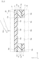
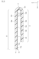
図3Aは本発明の第3実施形態におけるセンサ装置を示す平面展開図であり、図3Bは図3AのIIIB-IIIB線に沿ったセンサ装置の断面図である。
図4は本発明の第4実施形態におけるセンサ装置を示す平面展開図である。
図5は本発明の第5実施形態におけるセンサ装置を示す平面展開図である。
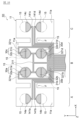
図6Aは本発明の第6実施形態におけるセンサ装置を示す平面展開図であり、図6Bは図6Aに示すセンサ装置の領域A,Cを折り曲げた状態を示す平面図であり、図6Cは図6BのVIC-VIC線に沿ったセンサ装置の断面図である。
図9は、本発明の第7実施形態におけるセンサ装置を示す平面展開図である。
図10は、本発明の第8実施形態におけるセンサ装置を示す平面展開図である。
11…絶縁性基材
12,12a~12d…センサ電極
121a~121d…引出配線
13…第1シールド部
13a~13c…領域
131,133,134…シールド電極
132…シールド配線
135…引出配線
136…対向部分
137…スリット
14,14a~14d…検知電極
141,141a~141d…引出配線
142…開口
15,15A,15B…スペーサ
151,152…開口
15a…第1面
15b…第2面
16,16a~16c…LED
17…カバーパネル
18…ベース基材
20…第2シールド部
30a~30c…センサ電極
31a~31d…入力電極
311…引出配線
31a~31d…受信電極
321a~321d…引出配線
40a~40d…遮断電極
41…引出配線
50…支持部材
51…クッション部材
R…所定領域
F…折り曲げ部
L1,L2…折り曲げ線
FIN…操作子
VF…仮想枠
Claims (12)
- 絶縁性基材と、
前記絶縁性基材の一方の主面に形成され、操作面側に配置される第1面に設けられたセンサ電極を備えたタッチセンサと、
前記第1面に設けられた遮断体と、
前記遮断体と対向配置され、前記第1面とは異なる第2面に設けられた検知電極と、を備え、
前記第1面の方が前記第2面よりも前記操作面側に位置し、
前記遮断体と前記検知電極とは、前記遮断体と前記検知電極とが接近することによる静電容量値の変化を検出する感圧センサを構成し、
前記遮断体は、前記操作面への操作子の接近に伴う前記操作子と前記検知電極との容量結合を遮り、
前記タッチセンサは、前記第1面に設けられた第1シールド部をさらに備え、
前記第1シールド部の少なくとも一部は、前記センサ電極の周囲の少なくとも一部に形成されており、
前記第1シールド部は、前記センサ電極を取り囲むように配置されており、
前記遮断体は、前記第1シールド部に含まれているセンサ装置。 - 請求項1に記載のセンサ装置であって、
前記センサ装置は、前記遮断体と前記検知電極との間の間隔を保持するスペーサをさらに備えており、
前記遮断体と前記検知電極は、前記操作子の押圧に応じて相互に接近可能であるセンサ装置。 - 請求項2に記載のセンサ装置であって、
前記スペーサは、前記遮断体と前記検知電極との間に配置された弾性体であるセンサ装置。 - 請求項2に記載のセンサ装置であって、
前記スペーサは、前記遮断体と前記検知電極との間に介在する開口を有するセンサ装置。 - 請求項1~4のいずれか一項に記載のセンサ装置であって、
前記遮断体は、平面視において、前記検知電極を覆っているセンサ装置。 - 請求項1~5のいずれか一項に記載のセンサ装置であって、
前記検知電極は、導電性材料により塗りつぶされているセンサ装置。 - 絶縁性基材と、
前記絶縁性基材の一方の主面に形成され、操作面側に配置される第1面に設けられたセンサ電極を備えたタッチセンサと、
前記第1面に設けられた遮断体と、
前記遮断体と対向配置され、前記第1面とは異なる第2面に設けられた検知電極と、を備え、
前記第1面の方が前記第2面よりも前記操作面側に位置し、
前記遮断体と前記検知電極とは、前記遮断体と前記検知電極とが接近することによる静電容量値の変化を検出する感圧センサを構成し、
前記遮断体は、前記操作面への操作子の接近に伴う前記操作子と前記検知電極との容量結合を遮り、
前記タッチセンサは、前記第1面に設けられた第1シールド部をさらに備え、
前記第1シールド部の少なくとも一部は、前記センサ電極の周囲の少なくとも一部に形成されており、
前記遮断体は、前記第1シールド部に含まれており、
前記センサ装置は、前記検知電極の周囲の少なくとも一部に形成された第2シールド部をさらに備えたセンサ装置。
- 請求項1~7のいずれか一項に記載のセンサ装置であって、
前記検知電極は、前記絶縁性基材のうち、前記センサ電極及び前記遮断体よりも外側であって所定領域を介在させた位置に形成され、
前記所定領域が屈曲されることにより、前記検知電極は前記遮断体と対向配置されるセンサ装置。 - 請求項1~8のいずれか一項に記載のセンサ装置であって、
前記タッチセンサは、複数の前記センサ電極を備え、
前記センサ装置は、複数の前記検知電極を備えており、
前記複数の検知電極は、平面視において、前記複数のセンサ電極の周囲に配置されているセンサ装置。 - 請求項9に記載のセンサ装置であって、
前記複数の前記センサ電極は、平面視において、前記複数の検知電極を包含し且つ前記複数の検知電極に接触する仮想枠の内側に配置されているセンサ装置。 - 絶縁性基材と、
前記絶縁性基材の一方の主面に形成され、操作面側に配置される第1面に設けられたセンサ電極を備えたタッチセンサと、
前記第1面に設けられた遮断体と、
前記遮断体と対向配置され、前記第1面とは異なる第2面に設けられた検知電極と、を備え、
前記第1面の方が前記第2面よりも前記操作面側に位置し、
前記遮断体と前記検知電極とは、前記遮断体と前記検知電極とが接近することによる静電容量値の変化を検出する感圧センサを構成し、
前記遮断体は、前記操作面への操作子の接近に伴う前記操作子と前記検知電極との容量結合を遮り、
前記タッチセンサは、前記第1面に設けられた第1シールド部をさらに備え、
前記第1シールド部の少なくとも一部は、前記センサ電極の周囲の少なくとも一部に形成されており、
前記遮断体は、前記第1シールド部に含まれており、
前記タッチセンサは、複数の前記センサ電極を備え、
前記センサ装置は、複数の前記検知電極を備えており、
前記複数の検知電極は、平面視において、前記複数のセンサ電極にそれぞれ対応するように配置されているセンサ装置。
- 絶縁性基材と、
前記絶縁性基材の一方の主面に形成され、操作面側に配置される第1面に設けられたセンサ電極を備えたタッチセンサと、
前記第1面に設けられた遮断体と、
前記遮断体と対向配置され、前記第1面とは異なる第2面に設けられた検知電極と、を備え、
前記第1面の方が前記第2面よりも前記操作面側に位置し、
前記遮断体と前記検知電極とは、前記遮断体と前記検知電極とが接近することによる静電容量値の変化を検出する感圧センサを構成し、
前記遮断体は、前記操作面への操作子の接近に伴う前記操作子と前記検知電極との容量結合を遮り、
前記タッチセンサは、前記第1面に設けられた第1シールド部をさらに備え、
前記第1シールド部の少なくとも一部は、前記センサ電極の周囲の少なくとも一部に形成されており、
前記遮断体は、前記第1シールド部に含まれており、
前記タッチセンサは、線状に延在するスリットを有する第1シールド部を備えており、
前記センサ装置は、前記検知電極に接続され、前記スリットを介して前記第1シールド部を通過する引出配線を備えたセンサ装置。
Applications Claiming Priority (1)
| Application Number | Priority Date | Filing Date | Title |
|---|---|---|---|
| PCT/JP2019/033725 WO2021038757A1 (ja) | 2019-08-28 | 2019-08-28 | センサ装置 |
Publications (2)
| Publication Number | Publication Date |
|---|---|
| JPWO2021038757A1 JPWO2021038757A1 (ja) | 2021-03-04 |
| JP7344968B2 true JP7344968B2 (ja) | 2023-09-14 |
Family
ID=74685315
Family Applications (1)
| Application Number | Title | Priority Date | Filing Date |
|---|---|---|---|
| JP2021541871A Active JP7344968B2 (ja) | 2019-08-28 | 2019-08-28 | センサ装置 |
Country Status (4)
| Country | Link |
|---|---|
| US (1) | US12287926B2 (ja) |
| EP (1) | EP4024426A4 (ja) |
| JP (1) | JP7344968B2 (ja) |
| WO (1) | WO2021038757A1 (ja) |
Families Citing this family (2)
| Publication number | Priority date | Publication date | Assignee | Title |
|---|---|---|---|---|
| DE102020216511A1 (de) * | 2020-12-22 | 2022-06-23 | Witte Automotive Gmbh | Elektronisches Sensormodul, Griffmodul und bewegliches Fahrzeugelement |
| JP2023023258A (ja) * | 2021-08-04 | 2023-02-16 | パナソニックIpマネジメント株式会社 | 静電スイッチの制御方法、及び、制御装置 |
Citations (4)
| Publication number | Priority date | Publication date | Assignee | Title |
|---|---|---|---|---|
| JP2005537610A (ja) | 2001-11-20 | 2005-12-08 | タッチセンサー テクノロジーズ,エルエルシー | 統合されたタッチ・センサおよび発光装置 |
| JP2007520120A (ja) | 2004-01-12 | 2007-07-19 | エーゲーオー エレクトロ・ゲレーテバウ ゲーエムベーハー | 容量性センサー素子を有する操作装置及びこのような操作装置を有する電気器具 |
| JP2010217967A (ja) | 2009-03-13 | 2010-09-30 | Alps Electric Co Ltd | 入力装置 |
| WO2019230634A1 (ja) | 2018-05-29 | 2019-12-05 | 信越ポリマー株式会社 | 感圧タッチセンサ及び感圧タッチセンサモジュール |
Family Cites Families (9)
| Publication number | Priority date | Publication date | Assignee | Title |
|---|---|---|---|---|
| US20060012944A1 (en) * | 2002-10-31 | 2006-01-19 | Mamigonians Hrand M | Mechanically operable electrical device |
| JP2009032570A (ja) | 2007-07-27 | 2009-02-12 | Fujikura Ltd | 人体接近検出装置 |
| JP5493739B2 (ja) | 2009-03-19 | 2014-05-14 | ソニー株式会社 | センサ装置及び情報処理装置 |
| US8730199B2 (en) * | 2009-09-04 | 2014-05-20 | Atmel Corporation | Capacitive control panel |
| JP5446626B2 (ja) | 2009-09-07 | 2014-03-19 | ソニー株式会社 | センサ装置及び情報処理装置 |
| JP5347913B2 (ja) * | 2009-11-06 | 2013-11-20 | ソニー株式会社 | センサ装置、電子機器、及びセンサ装置の製造方法 |
| GB2528855A (en) * | 2014-07-31 | 2016-02-10 | Touchnetix Ltd | Displacement sensing apparatus and methods |
| CN107357471A (zh) | 2016-05-09 | 2017-11-17 | 新益先创科技股份有限公司 | 感测装置 |
| FR3060733B1 (fr) * | 2016-12-16 | 2019-01-25 | Fogale Nanotech | Dispositif et procede de detection de l'approche et/ou de contact, et de l'appui d'un objet, relativement a une surface de detection |
-
2019
- 2019-08-28 WO PCT/JP2019/033725 patent/WO2021038757A1/ja not_active Ceased
- 2019-08-28 JP JP2021541871A patent/JP7344968B2/ja active Active
- 2019-08-28 EP EP19943426.7A patent/EP4024426A4/en active Pending
- 2019-08-28 US US17/638,008 patent/US12287926B2/en active Active
Patent Citations (4)
| Publication number | Priority date | Publication date | Assignee | Title |
|---|---|---|---|---|
| JP2005537610A (ja) | 2001-11-20 | 2005-12-08 | タッチセンサー テクノロジーズ,エルエルシー | 統合されたタッチ・センサおよび発光装置 |
| JP2007520120A (ja) | 2004-01-12 | 2007-07-19 | エーゲーオー エレクトロ・ゲレーテバウ ゲーエムベーハー | 容量性センサー素子を有する操作装置及びこのような操作装置を有する電気器具 |
| JP2010217967A (ja) | 2009-03-13 | 2010-09-30 | Alps Electric Co Ltd | 入力装置 |
| WO2019230634A1 (ja) | 2018-05-29 | 2019-12-05 | 信越ポリマー株式会社 | 感圧タッチセンサ及び感圧タッチセンサモジュール |
Also Published As
| Publication number | Publication date |
|---|---|
| WO2021038757A1 (ja) | 2021-03-04 |
| US20220276732A1 (en) | 2022-09-01 |
| EP4024426A4 (en) | 2023-05-24 |
| US12287926B2 (en) | 2025-04-29 |
| JPWO2021038757A1 (ja) | 2021-03-04 |
| EP4024426A1 (en) | 2022-07-06 |
Similar Documents
| Publication | Publication Date | Title |
|---|---|---|
| US10007380B2 (en) | Touch input device with edge support member | |
| KR101598412B1 (ko) | 전극 시트 및 터치 입력 장치 | |
| JP7198469B2 (ja) | スマートフォン | |
| EP3089008B1 (en) | Touch input device | |
| US20140293163A1 (en) | Touch panel | |
| CN106155411B (zh) | 触摸屏、触摸面板、显示装置以及电子设备 | |
| US10359890B2 (en) | Touch screen, touch panel, and display apparatus | |
| JP3144241U (ja) | コンデンサー式タッチパッド | |
| JP5472858B2 (ja) | タッチスイッチ | |
| EP2602698A1 (en) | Touch panel | |
| JP7344968B2 (ja) | センサ装置 | |
| JP5750466B2 (ja) | 静電容量式入力装置 | |
| KR20130045801A (ko) | 터치 패널 및 그것의 제조 방법 | |
| JP7026525B2 (ja) | センサ装置 | |
| JP3144563U (ja) | コンデンサ式タッチパッド | |
| JP2019087060A (ja) | タッチパネル | |
| EP2972709B1 (en) | Capacitive sensor electrode | |
| KR20160098988A (ko) | 터치 입력 장치 | |
| KR101865301B1 (ko) | 터치 입력 장치 | |
| JP5908637B2 (ja) | 静電容量式入力装置 | |
| JP2020149563A (ja) | タッチスクリーン、タッチパネル、表示装置および電子機器 | |
| CN110506251B (zh) | 触摸传感器 | |
| JP6578860B2 (ja) | 静電容量式タッチデバイス | |
| KR20140081241A (ko) | 터치 패널 | |
| JP2014170341A (ja) | 静電容量式入力装置 |
Legal Events
| Date | Code | Title | Description |
|---|---|---|---|
| A621 | Written request for application examination |
Free format text: JAPANESE INTERMEDIATE CODE: A621 Effective date: 20220216 |
|
| A131 | Notification of reasons for refusal |
Free format text: JAPANESE INTERMEDIATE CODE: A131 Effective date: 20221129 |
|
| A601 | Written request for extension of time |
Free format text: JAPANESE INTERMEDIATE CODE: A601 Effective date: 20230126 |
|
| A521 | Request for written amendment filed |
Free format text: JAPANESE INTERMEDIATE CODE: A523 Effective date: 20230213 |
|
| A131 | Notification of reasons for refusal |
Free format text: JAPANESE INTERMEDIATE CODE: A131 Effective date: 20230425 |
|
| A521 | Request for written amendment filed |
Free format text: JAPANESE INTERMEDIATE CODE: A523 Effective date: 20230620 |
|
| TRDD | Decision of grant or rejection written | ||
| A01 | Written decision to grant a patent or to grant a registration (utility model) |
Free format text: JAPANESE INTERMEDIATE CODE: A01 Effective date: 20230808 |
|
| A61 | First payment of annual fees (during grant procedure) |
Free format text: JAPANESE INTERMEDIATE CODE: A61 Effective date: 20230904 |
|
| R151 | Written notification of patent or utility model registration |
Ref document number: 7344968 Country of ref document: JP Free format text: JAPANESE INTERMEDIATE CODE: R151 |