JP7360246B2 - display device - Google Patents
display device Download PDFInfo
- Publication number
- JP7360246B2 JP7360246B2 JP2019047597A JP2019047597A JP7360246B2 JP 7360246 B2 JP7360246 B2 JP 7360246B2 JP 2019047597 A JP2019047597 A JP 2019047597A JP 2019047597 A JP2019047597 A JP 2019047597A JP 7360246 B2 JP7360246 B2 JP 7360246B2
- Authority
- JP
- Japan
- Prior art keywords
- heating resistor
- electrode
- light emitting
- pixel
- display device
- Prior art date
- Legal status (The legal status is an assumption and is not a legal conclusion. Google has not performed a legal analysis and makes no representation as to the accuracy of the status listed.)
- Active
Links
Images




Classifications
-
- G—PHYSICS
- G09—EDUCATION; CRYPTOGRAPHY; DISPLAY; ADVERTISING; SEALS
- G09G—ARRANGEMENTS OR CIRCUITS FOR CONTROL OF INDICATING DEVICES USING STATIC MEANS TO PRESENT VARIABLE INFORMATION
- G09G3/00—Control arrangements or circuits, of interest only in connection with visual indicators other than cathode-ray tubes
- G09G3/20—Control arrangements or circuits, of interest only in connection with visual indicators other than cathode-ray tubes for presentation of an assembly of a number of characters, e.g. a page, by composing the assembly by combination of individual elements arranged in a matrix no fixed position being assigned to or needed to be assigned to the individual characters or partial characters
- G09G3/22—Control arrangements or circuits, of interest only in connection with visual indicators other than cathode-ray tubes for presentation of an assembly of a number of characters, e.g. a page, by composing the assembly by combination of individual elements arranged in a matrix no fixed position being assigned to or needed to be assigned to the individual characters or partial characters using controlled light sources
- G09G3/30—Control arrangements or circuits, of interest only in connection with visual indicators other than cathode-ray tubes for presentation of an assembly of a number of characters, e.g. a page, by composing the assembly by combination of individual elements arranged in a matrix no fixed position being assigned to or needed to be assigned to the individual characters or partial characters using controlled light sources using electroluminescent panels
- G09G3/32—Control arrangements or circuits, of interest only in connection with visual indicators other than cathode-ray tubes for presentation of an assembly of a number of characters, e.g. a page, by composing the assembly by combination of individual elements arranged in a matrix no fixed position being assigned to or needed to be assigned to the individual characters or partial characters using controlled light sources using electroluminescent panels semiconductive, e.g. using light-emitting diodes [LED]
-
- H—ELECTRICITY
- H10—SEMICONDUCTOR DEVICES; ELECTRIC SOLID-STATE DEVICES NOT OTHERWISE PROVIDED FOR
- H10W—GENERIC PACKAGES, INTERCONNECTIONS, CONNECTORS OR OTHER CONSTRUCTIONAL DETAILS OF DEVICES COVERED BY CLASS H10
- H10W90/00—Package configurations
-
- G—PHYSICS
- G09—EDUCATION; CRYPTOGRAPHY; DISPLAY; ADVERTISING; SEALS
- G09F—DISPLAYING; ADVERTISING; SIGNS; LABELS OR NAME-PLATES; SEALS
- G09F9/00—Indicating arrangements for variable information in which the information is built-up on a support by selection or combination of individual elements
- G09F9/30—Indicating arrangements for variable information in which the information is built-up on a support by selection or combination of individual elements in which the desired character or characters are formed by combining individual elements
-
- H—ELECTRICITY
- H10—SEMICONDUCTOR DEVICES; ELECTRIC SOLID-STATE DEVICES NOT OTHERWISE PROVIDED FOR
- H10H—INORGANIC LIGHT-EMITTING SEMICONDUCTOR DEVICES HAVING POTENTIAL BARRIERS
- H10H29/00—Integrated devices, or assemblies of multiple devices, comprising at least one light-emitting semiconductor element covered by group H10H20/00
- H10H29/10—Integrated devices comprising at least one light-emitting semiconductor component covered by group H10H20/00
- H10H29/14—Integrated devices comprising at least one light-emitting semiconductor component covered by group H10H20/00 comprising multiple light-emitting semiconductor components
- H10H29/142—Two-dimensional arrangements, e.g. asymmetric LED layout
-
- H—ELECTRICITY
- H10—SEMICONDUCTOR DEVICES; ELECTRIC SOLID-STATE DEVICES NOT OTHERWISE PROVIDED FOR
- H10W—GENERIC PACKAGES, INTERCONNECTIONS, CONNECTORS OR OTHER CONSTRUCTIONAL DETAILS OF DEVICES COVERED BY CLASS H10
- H10W40/00—Arrangements for thermal protection or thermal control
-
- G—PHYSICS
- G09—EDUCATION; CRYPTOGRAPHY; DISPLAY; ADVERTISING; SEALS
- G09G—ARRANGEMENTS OR CIRCUITS FOR CONTROL OF INDICATING DEVICES USING STATIC MEANS TO PRESENT VARIABLE INFORMATION
- G09G2300/00—Aspects of the constitution of display devices
- G09G2300/04—Structural and physical details of display devices
- G09G2300/0421—Structural details of the set of electrodes
- G09G2300/0426—Layout of electrodes and connections
-
- G—PHYSICS
- G09—EDUCATION; CRYPTOGRAPHY; DISPLAY; ADVERTISING; SEALS
- G09G—ARRANGEMENTS OR CIRCUITS FOR CONTROL OF INDICATING DEVICES USING STATIC MEANS TO PRESENT VARIABLE INFORMATION
- G09G2300/00—Aspects of the constitution of display devices
- G09G2300/04—Structural and physical details of display devices
- G09G2300/0439—Pixel structures
- G09G2300/0452—Details of colour pixel setup, e.g. pixel composed of a red, a blue and two green components
-
- G—PHYSICS
- G09—EDUCATION; CRYPTOGRAPHY; DISPLAY; ADVERTISING; SEALS
- G09G—ARRANGEMENTS OR CIRCUITS FOR CONTROL OF INDICATING DEVICES USING STATIC MEANS TO PRESENT VARIABLE INFORMATION
- G09G2300/00—Aspects of the constitution of display devices
- G09G2300/08—Active matrix structure, i.e. with use of active elements, inclusive of non-linear two terminal elements, in the pixels together with light emitting or modulating elements
- G09G2300/0809—Several active elements per pixel in active matrix panels
- G09G2300/0819—Several active elements per pixel in active matrix panels used for counteracting undesired variations, e.g. feedback or autozeroing
-
- G—PHYSICS
- G09—EDUCATION; CRYPTOGRAPHY; DISPLAY; ADVERTISING; SEALS
- G09G—ARRANGEMENTS OR CIRCUITS FOR CONTROL OF INDICATING DEVICES USING STATIC MEANS TO PRESENT VARIABLE INFORMATION
- G09G2300/00—Aspects of the constitution of display devices
- G09G2300/08—Active matrix structure, i.e. with use of active elements, inclusive of non-linear two terminal elements, in the pixels together with light emitting or modulating elements
- G09G2300/0809—Several active elements per pixel in active matrix panels
- G09G2300/0842—Several active elements per pixel in active matrix panels forming a memory circuit, e.g. a dynamic memory with one capacitor
- G09G2300/0852—Several active elements per pixel in active matrix panels forming a memory circuit, e.g. a dynamic memory with one capacitor being a dynamic memory with more than one capacitor
-
- G—PHYSICS
- G09—EDUCATION; CRYPTOGRAPHY; DISPLAY; ADVERTISING; SEALS
- G09G—ARRANGEMENTS OR CIRCUITS FOR CONTROL OF INDICATING DEVICES USING STATIC MEANS TO PRESENT VARIABLE INFORMATION
- G09G2320/00—Control of display operating conditions
- G09G2320/04—Maintaining the quality of display appearance
- G09G2320/041—Temperature compensation
Landscapes
- Engineering & Computer Science (AREA)
- Physics & Mathematics (AREA)
- General Physics & Mathematics (AREA)
- Theoretical Computer Science (AREA)
- Computer Hardware Design (AREA)
- Control Of Indicators Other Than Cathode Ray Tubes (AREA)
- Control Of El Displays (AREA)
- Electroluminescent Light Sources (AREA)
- Devices For Indicating Variable Information By Combining Individual Elements (AREA)
Description
本発明は、表示装置に関する。 The present invention relates to a display device.
近年、表示素子として微小サイズの発光ダイオード(マイクロLED(micro LED))を用いたディスプレイが注目されている(例えば、特許文献1参照)。複数の発光ダイオードは、アレイ基板(特許文献1ではドライババックプレーン)に接続され、アレイ基板は、発光ダイオードを駆動するための画素回路(特許文献1では電子制御回路)を備える。 In recent years, displays using microscopic light emitting diodes (micro LEDs) as display elements have attracted attention (for example, see Patent Document 1). The plurality of light emitting diodes are connected to an array substrate (driver backplane in Patent Document 1), and the array substrate includes a pixel circuit (electronic control circuit in Patent Document 1) for driving the light emitting diodes.
発光ダイオードは、温度上昇に伴い発光効率が低下する。このため、発光ダイオードを利用した表示装置では、温度上昇に伴い輝度が低下し、表示特性が低下する可能性がある。 The light emitting efficiency of light emitting diodes decreases as the temperature rises. Therefore, in a display device using a light emitting diode, brightness may decrease as the temperature rises, and display characteristics may deteriorate.
本発明は、表示特性の低下を抑制することができる表示装置を提供することを目的とする。 An object of the present invention is to provide a display device that can suppress deterioration of display characteristics.
本発明の一態様の表示装置は、基板と、前記基板に設けられた複数の画素と、複数の前記画素の各々に設けられる発光素子と、前記基板に設けられ、前記発光素子に駆動信号を供給する画素回路と、前記画素回路に設けられた発熱抵抗体と、を有する。 A display device according to one embodiment of the present invention includes a substrate, a plurality of pixels provided on the substrate, a light-emitting element provided in each of the plurality of pixels, and a display device provided on the substrate and configured to send a drive signal to the light-emitting element. and a heating resistor provided in the pixel circuit.
本発明を実施するための形態(実施形態)につき、図面を参照しつつ詳細に説明する。以下の実施形態に記載した内容により本発明が限定されるものではない。また、以下に記載した構成要素には、当業者が容易に想定できるもの、実質的に同一のものが含まれる。さらに、以下に記載した構成要素は適宜組み合わせることが可能である。なお、開示はあくまで一例にすぎず、当業者において、発明の主旨を保っての適宜変更について容易に想到し得るものについては、当然に本発明の範囲に含有されるものである。また、図面は説明をより明確にするため、実際の態様に比べ、各部の幅、厚さ、形状等について模式的に表される場合があるが、あくまで一例であって、本発明の解釈を限定するものではない。また、本明細書と各図において、既出の図に関して前述したものと同様の要素には、同一の符号を付して、詳細な説明を適宜省略することがある。 DESCRIPTION OF THE PREFERRED EMBODIMENTS Modes (embodiments) for carrying out the present invention will be described in detail with reference to the drawings. The present invention is not limited to the contents described in the following embodiments. Further, the constituent elements described below include those that can be easily assumed by those skilled in the art and those that are substantially the same. Furthermore, the components described below can be combined as appropriate. It should be noted that the disclosure is merely an example, and any modifications that can be easily made by those skilled in the art while maintaining the gist of the invention are naturally included within the scope of the present invention. In addition, in order to make the explanation clearer, the drawings may schematically represent the width, thickness, shape, etc. of each part compared to the actual aspect, but these are only examples, and the interpretation of the present invention is It is not limited. In addition, in this specification and each figure, the same elements as those described above with respect to the previously shown figures are denoted by the same reference numerals, and detailed explanations may be omitted as appropriate.
本明細書及び特許請求の範囲において、ある構造体の上に他の構造体を配置する態様を表現するにあたり、単に「上に」と表記する場合、特に断りの無い限りは、ある構造体に接するように、直上に他の構造体を配置する場合と、ある構造体の上方に、さらに別の構造体を介して他の構造体を配置する場合との両方を含むものとする。 In this specification and the claims, when expressing a mode in which another structure is placed on top of a certain structure, when it is simply expressed as "above", unless otherwise specified, This includes both a case in which another structure is placed directly above a certain structure so as to be in contact with the structure, and a case in which another structure is placed above a certain structure via another structure.
(第1実施形態)
図1は、第1実施形態に係る表示装置を模式的に示す平面図である。図1に示すように、表示装置1は、アレイ基板2と、画素Pixと、駆動回路12と、駆動IC(Integrated Circuit)210と、カソード配線60と、を含む。アレイ基板2は、各画素Pixを駆動するための駆動回路基板であり、バックプレーン又はアクティブマトリックス基板とも呼ばれる。アレイ基板2は、基板21、複数のトランジスタ、複数の容量及び各種配線等を有する。
(First embodiment)
FIG. 1 is a plan view schematically showing a display device according to a first embodiment. As shown in FIG. 1, the
図1に示すように、表示装置1は、表示領域AAと、周辺領域GAとを有する。表示領域AAは、複数の画素Pixと重なって配置され、画像を表示する領域である。周辺領域GAは、複数の画素Pixと重ならない領域であり、表示領域AAの外側に配置される。
As shown in FIG. 1, the
複数の画素Pixは、基板21の表示領域AAにおいて、第1方向Dx及び第2方向Dyに配列される。なお、第1方向Dx及び第2方向Dyは、基板21の表面に対して平行な方向である。第1方向Dxは、第2方向Dyと直交する。ただし、第1方向Dxは、第2方向Dyと直交しないで交差してもよい。第3方向Dzは、第1方向Dx及び第2方向Dyと直交する方向である。第3方向Dzは、例えば、基板21の法線方向に対応する。なお、以下、平面視とは、第3方向Dzから見た場合の位置関係を示す。
The plurality of pixels Pix are arranged in the first direction Dx and the second direction Dy in the display area AA of the
駆動回路12は、駆動IC210からの各種制御信号に基づいて複数のゲート線(例えば、発光制御走査線BG、リセット制御走査線RG、初期化制御走査線IG、書込制御走査線SG及び発熱制御走査線HG(図3参照))を駆動する回路である。駆動回路12は、複数のゲート線を順次又は同時に選択し、選択されたゲート線にゲート駆動信号を供給する。これにより、駆動回路12は、ゲート線に接続された複数の画素Pixを選択する。
The
駆動IC210は、表示装置1の表示を制御する回路である。駆動IC210は、基板21の周辺領域GAにCOG(Chip On Glass)として実装される。これに限定されず、駆動IC210は、基板21の周辺領域GAに接続されたフレキシブルプリント基板やリジット基板の上にCOF(Chip On Film)として実装されてもよい。
The drive IC 210 is a circuit that controls the display of the
カソード配線60は、基板21の周辺領域GAに設けられる。カソード配線60は、表示領域AAの複数の画素Pix及び周辺領域GAの駆動回路12を囲んで設けられる。複数の発光素子3のカソードは、共通のカソード配線60に電気的に接続され、固定電位(例えば、グランド電位)が供給される。より具体的には、発光素子3のカソード端子32(図7参照)は、カソード電極22(第2電極)を介して、カソード配線60に接続される。
The
図2は、複数の副画素を示す平面図である。図2に示すように、1つの画素Pixは、複数の副画素49を含む。例えば、画素Pixは、第1副画素49Rと、第2副画素49Gと、第3副画素49Bとを有する。第1副画素49Rは、第1色としての原色の赤色を表示する。第2副画素49Gは、第2色としての原色の緑色を表示する。第3副画素49Bは、第3色としての原色の青色を表示する。図2に示すように、1つの画素Pixにおいて、第1副画素49Rと第3副画素49Bは第1方向Dxで並ぶ。また、第2副画素49Gと第3副画素49Bは第2方向Dyで並ぶ。なお、第1色、第2色、第3色は、それぞれ赤色、緑色、青色に限られず、補色などの任意の色を選択することができる。以下において、第1副画素49Rと、第2副画素49Gと、第3副画素49Bとをそれぞれ区別する必要がない場合、副画素49という。
FIG. 2 is a plan view showing a plurality of subpixels. As shown in FIG. 2, one pixel Pix includes a plurality of
副画素49は、それぞれ発光素子3と、アノード電極23(第1電極)と、を有する。表示装置1は、第1副画素49R、第2副画素49G及び第3副画素49Bにおいて、発光素子3R、3G、3Bごとに異なる光(例えば、赤色、緑色、青色の光)を出射することで画像を表示する。発光素子3は、複数の副画素49の各々に設けられる。発光素子3は、平面視で、3μm以上、300μm以下程度の大きさを有する発光ダイオード(LED:Light Emitting Diode)チップであり、マイクロLED(micro LED)と呼ばれる。各画素にマイクロLEDを備える表示装置1は、マイクロLED表示装置とも呼ばれる。なお、マイクロLEDのマイクロは、発光素子3の大きさを限定するものではない。
Each
なお、複数の発光素子3は、4色以上の異なる光を出射してもよい。また、複数の副画素49の配置は、図2に示す構成に限定されない。例えば、第1副画素49Rは第2副画素49Gと第1方向Dxに隣り合っていてもよい。また、第1副画素49R、第2副画素49G及び第3副画素49Bが、この順で第1方向Dxに繰り返し配列されてもよい。
Note that the plurality of
図3は、画素回路を示す回路図である。図3に示す画素回路PICAは、第1副画素49R、第2副画素49G及び第3副画素49Bのそれぞれに設けられる。画素回路PICAは、基板21に設けられ、駆動信号(電流)を発光素子3に供給する回路である。なお、図3において、画素回路PICAについての説明は、第1副画素49R、第2副画素49G及び第3副画素49Bのそれぞれが有する画素回路PICAに適用できる。
FIG. 3 is a circuit diagram showing a pixel circuit. The pixel circuit PICA shown in FIG. 3 is provided for each of the
図3に示すように、画素回路PICAは、発光素子3と、6つのトランジスタと、2つの容量と、発熱抵抗体28と、を含む。具体的には、画素回路PICAは、発光制御トランジスタBCT、初期化トランジスタIST、書込トランジスタSST、リセットトランジスタRST、駆動トランジスタDRT及び発熱制御トランジスタHSTを含む。一部のトランジスタは、隣接する複数の副画素49で共有されていてもよい。例えば、発光制御トランジスタBCTは、共通配線を介して、3つの副画素49で共有されていてもよい。また、リセットトランジスタRSTは、周辺領域GAに設けられ、例えば副画素49の各行に1つ設けられていてもよい。この場合、リセットトランジスタRSTは、共通配線を介して複数の駆動トランジスタDRTのソースに接続される。
As shown in FIG. 3, the pixel circuit PICA includes a
画素回路PICAが有する複数のトランジスタは、それぞれn型TFT(Thin Film Transistor)で構成される。ただし、これに限定されず、各トランジスタは、それぞれp型TFTで構成されてもよい。p型TFTを用いる場合は、適宜電源電位や保持容量Cs1及び容量Cs2の接続を適合させてもよい。 Each of the plurality of transistors included in the pixel circuit PICA is composed of an n-type TFT (Thin Film Transistor). However, the present invention is not limited thereto, and each transistor may be composed of a p-type TFT. When using a p-type TFT, the power supply potential and the connection of the holding capacitor Cs1 and the capacitor Cs2 may be adjusted as appropriate.
発光制御走査線BGは、発光制御トランジスタBCTのゲートに接続される。初期化制御走査線IGは、初期化トランジスタISTのゲートに接続される。書込制御走査線SGは、書込トランジスタSSTのゲートに接続される。リセット制御走査線RGは、リセットトランジスタRSTのゲートに接続される。発熱制御走査線HGは、発熱制御トランジスタHSTのゲートに接続される。 The light emission control scanning line BG is connected to the gate of the light emission control transistor BCT. Initialization control scan line IG is connected to the gate of initialization transistor IST. Write control scan line SG is connected to the gate of write transistor SST. Reset control scanning line RG is connected to the gate of reset transistor RST. The heat generation control scanning line HG is connected to the gate of the heat generation control transistor HST.
発光制御走査線BG、初期化制御走査線IG、書込制御走査線SG、リセット制御走査線RG及び発熱制御走査線HGは、それぞれ、周辺領域GAに設けられた駆動回路12(図1参照)に接続される。駆動回路12は、発光制御走査線BG、初期化制御走査線IG、書込制御走査線SG、リセット制御走査線RG及び発熱制御走査線HGに、それぞれ、発光制御信号Vbg、初期化制御信号Vig、書込制御信号Vsg、リセット制御信号Vrg及び発熱制御信号Vhgを供給する。
The light emission control scanning line BG, the initialization control scanning line IG, the write control scanning line SG, the reset control scanning line RG, and the heat generation control scanning line HG are each connected to the
駆動IC210(図1参照)は、第1副画素49R、第2副画素49G及び第3副画素49Bのそれぞれの画素回路PICAに、時分割で映像信号Vsigを供給する。第1副画素49R、第2副画素49G及び第3副画素49Bの各列と、駆動IC210との間には、マルチプレクサ等のスイッチ回路が設けられる。映像信号Vsigは、映像信号線L2を介して書込トランジスタSSTに供給される。また、駆動IC210は、リセット信号線L3を介して、リセット電源電位VrstをリセットトランジスタRSTに供給する。駆動IC210は、初期化信号線L4を介して、初期化電位Viniを初期化トランジスタISTに供給する。
The drive IC 210 (see FIG. 1) supplies the video signal Vsig to each pixel circuit PICA of the
発光制御トランジスタBCT、初期化トランジスタIST、書込トランジスタSST、リセットトランジスタRST及び発熱制御トランジスタHSTは、2ノード間の導通と非導通とを選択するスイッチング素子として機能する。駆動トランジスタDRTは、ゲートとドレインとの間の電圧に応じて、発光素子3に流れる電流を制御する電流制御素子として機能する。
The light emission control transistor BCT, initialization transistor IST, write transistor SST, reset transistor RST, and heat generation control transistor HST function as switching elements that select conduction and non-conduction between two nodes. The drive transistor DRT functions as a current control element that controls the current flowing through the
発光素子3のカソード(カソード端子32)は、カソード電源線L10(第2電源線)に接続される。また、発光素子3のアノード(アノード端子33)は、駆動トランジスタDRT及び発光制御トランジスタBCTを介してアノード電源線L1(第1電源線)に接続される。アノード電源線L1には、アノード電源電位PVDD(第1電位)が供給される。カソード電源線L10には、カソード電源電位PVSS(第2電位)が供給される。アノード電源電位PVDDは、カソード電源電位PVSSよりも高い電位である。カソード電源線L10は、カソード配線60を含む。なお、発光素子3の発光動作については後述する。
The cathode (cathode terminal 32) of the
発熱抵抗体28の一端側28e1は、アノード電極23に接続される。発熱抵抗体28の他端側28e2は、発熱制御トランジスタHSTを介してアノード電源線L1に電気的に接続される。
One end 28e1 of the
また、画素回路PICAは、保持容量Cs1及び容量Cs2を含む。保持容量Cs1は、駆動トランジスタDRTのゲートとソースとの間に形成される容量である。容量Cs2は、駆動トランジスタDRTのソース及び発光素子3のアノードと、カソード電源線L10との間に形成される付加容量である。
Further, the pixel circuit PICA includes a storage capacitor Cs1 and a capacitor Cs2. The holding capacitor Cs1 is a capacitor formed between the gate and source of the drive transistor DRT. The capacitor Cs2 is an additional capacitor formed between the source of the drive transistor DRT, the anode of the
図4は、表示装置の動作例を示すタイミングチャートである。図4に示す期間G1から期間G4のそれぞれが1水平期間である。なお、図4では、1行目の副画素49から4行目の副画素49を駆動する動作を示しているが、5行目以降、最終行の副画素49まで継続して駆動される。また、以下の説明では、1行目の副画素49から最終行の副画素49までの駆動を行う期間をフレーム期間1Fと表す。
FIG. 4 is a timing chart showing an example of the operation of the display device. Each of the periods G1 to G4 shown in FIG. 4 is one horizontal period. Note that although FIG. 4 shows the operation of driving the
図4に示す期間t0から期間t5までの動作例について、以下詳細に説明する。期間t0は、前フレーム発光期間である。つまり、あるフレーム期間1Fでの処理が開始されるまでの期間t0では、副画素49は、前フレームの発光状態を継続している。
An example of the operation from period t0 to period t5 shown in FIG. 4 will be described in detail below. The period t0 is a previous frame light emission period. That is, during the period t0 until the processing in a
次に、期間t1は、駆動トランジスタDRTのソース初期化期間である。具体的には、期間t1では、駆動回路12から供給される各制御信号により、発光制御走査線BG1の電位がL(ロウ)レベルとなり、リセット制御走査線RG1の電位がHレベルとなる。これにより、発光制御トランジスタBCTがオフ(非導通状態)となり、リセットトランジスタRSTがオン(導通状態)となる。
Next, period t1 is a source initialization period of drive transistor DRT. Specifically, in period t1, each control signal supplied from the
なお、発光制御走査線BG1は、1行目の副画素49に接続された発光制御走査線BGを示し、発光制御走査線BG2は、2行目の副画素49に接続された発光制御走査線BGを示す。発光制御走査線BG3は、3行目の副画素49に接続された発光制御走査線BGを示し、発光制御走査線BG4は、4行目の副画素49に接続された発光制御走査線BGを示す。リセット制御走査線RG1、RG2、RG3、RG4等の各走査線も同様である。
Note that the emission control scanning line BG1 indicates the emission control scanning line BG connected to the
期間t1では、1行目に属する副画素49において、アノード電源線L1からの電流が発光制御トランジスタBCTにより遮断される。発光素子3の発光が停止するとともに、副画素49内に残留していた電荷が、リセットトランジスタRSTを通じて外部に流れる。これにより、駆動トランジスタDRTのソースがリセット電源電位Vrstに固定される。リセット電源電位Vrstは、カソード電源電位PVSSに対して所定の電位差を有して設定される。この場合、リセット電源電位Vrstとカソード電源電位PVSSとの電位差は、発光素子3が発光を開始する電位差よりも小さい。
In the period t1, the current from the anode power supply line L1 is cut off by the light emission control transistor BCT in the
次に、期間t2は、駆動トランジスタDRTのゲート初期化期間である。具体的には、期間t2では、駆動回路12から供給される各制御信号により、初期化制御走査線IG1の電位がHレベルとなる。初期化トランジスタISTは、オンとなる。1行目に属する副画素49において、初期化トランジスタISTを介して駆動トランジスタDRTのゲートが初期化電位Viniに固定される。初期化電位Viniは、リセット電源電位Vrstに対して、駆動トランジスタDRTのしきい値よりも大きい電位を有している。このため、駆動トランジスタDRTはオンとなる。ただし、期間t2では、発光制御トランジスタBCTがオフの状態を維持しているので、駆動トランジスタDRTには電流が流れない。
Next, a period t2 is a gate initialization period of the drive transistor DRT. Specifically, in the period t2, each control signal supplied from the
次に、期間t3は、オフセットキャンセル動作期間である。具体的には、期間t3では、駆動回路12から供給される各制御信号により、発光制御走査線BG1の電位がHレベルとなり、リセット制御走査線RG1の電位がLレベルとなる。これにより、発光制御トランジスタBCTがオンとなり、リセットトランジスタRSTがオフとなる。
Next, period t3 is an offset cancellation operation period. Specifically, in period t3, each control signal supplied from the
駆動トランジスタDRTは、期間t2の動作によりオン状態となっている。このため、アノード電源線L1(アノード電源電位PVDD)から、発光制御トランジスタBCTを介して駆動トランジスタDRTに電流が供給される。 The drive transistor DRT is in the on state due to the operation during the period t2. Therefore, current is supplied from the anode power supply line L1 (anode power supply potential PVDD) to the drive transistor DRT via the light emission control transistor BCT.
この段階では、発光素子3のアノードとカソードとの間の電圧は、発光開始電圧よりも小さいので、電流が流れない。したがって、アノード電源電位PVDDによって駆動トランジスタDRTのソースが充電され、ソースの電位が上昇する。駆動トランジスタDRTのゲート電位は、初期化電位Viniとなっている。このため、駆動トランジスタDRTのソース電位が(Vini-Vth)となった段階で駆動トランジスタDRTがオフになり、電位の上昇が停止する。ここで、Vthは、駆動トランジスタDRTのしきい値電圧Vthである。
At this stage, the voltage between the anode and cathode of the
しきい値電圧Vthは、副画素49ごとにばらつきがある。このため、電位の上昇が停止したときの駆動トランジスタDRTのソースの電位は、副画素49ごとに異なる。つまり、期間t3の動作によって、各副画素49で、駆動トランジスタDRTのしきい値電圧Vthに相当する電圧が取得される。このとき、発光素子3には、((Vini-Vth)-PVSS)の電圧が印加される。この電圧は、発光素子3の発光開始電圧よりも小さいので、発光素子3には電流が流れない。
The threshold voltage Vth varies from subpixel to
次に、期間t4は、映像信号書込動作期間である。具体的には、期間t4では、駆動回路12から供給される各制御信号により、発光制御走査線BG1の電位がLレベルとなり、初期化制御走査線IG1の電位がLレベルとなり、書込制御走査線SG1がHレベルとなる。
Next, period t4 is a video signal writing operation period. Specifically, in period t4, each control signal supplied from the
これにより、発光制御トランジスタBCTがオフになり、初期化トランジスタISTがオフになり、書込トランジスタSSTがオンになる。期間t4では、1行目に属する副画素49において、映像信号Vsigが駆動トランジスタDRTのゲートに入力される。駆動トランジスタDRTのゲート電位は、初期化電位Viniから映像信号Vsigの電位に変化する。一方、駆動トランジスタDRTのソースの電位は、(Vini-Vth)を維持している。この結果、駆動トランジスタDRTのゲートとソースとの間の電圧は、(Vsig-(Vini-Vth))となり、副画素49間のしきい値電圧Vthのばらつきが反映されたものとなる。
As a result, the light emission control transistor BCT is turned off, the initialization transistor IST is turned off, and the write transistor SST is turned on. In the period t4, the video signal Vsig is input to the gate of the drive transistor DRT in the
映像信号線L2は、第2方向Dy(図1参照)に延在し、同列に属する複数行の副画素49に接続される。このため、映像書込動作を行う期間t4は、1行ごとに実施される。
The video signal line L2 extends in the second direction Dy (see FIG. 1) and is connected to multiple rows of
次に、期間t5は、発光動作期間である。具体的には、期間t5では、駆動回路12から供給される各制御信号により、発光制御走査線BG1の電位がHレベルとなり、書込制御走査線SG1がLレベルとなる。これにより、発光制御トランジスタBCTがオンになり、書込トランジスタSSTがオフになる。アノード電源線L1(アノード電源電位PVDD)から、発光制御トランジスタBCTを介して駆動トランジスタDRTに電流が供給される。
Next, period t5 is a light emission operation period. Specifically, in period t5, each control signal supplied from the
駆動トランジスタDRTは、期間t4までに設定されたゲートソース間の電圧に応じた電流を、発光素子3に供給する。発光素子3は、この電流に応じた輝度で発光する。このとき、発光素子3のアノードとカソードとの間の電圧は、駆動トランジスタDRTを通して供給された電流値に応じた電圧となる。これにより、発光素子3のアノードの電位が上昇する。ここで、駆動トランジスタDRTのゲートとソースとの間の電圧は、保持容量Cs1によって保持される。このため、保持容量Cs1のカップリングにより、発光素子3のアノードの電位上昇に伴って、駆動トランジスタDRTのゲート電位も上昇する。
The drive transistor DRT supplies the
実際には、駆動トランジスタDRTのゲートには、保持容量Cs1に加えて容量Cs2等の付加容量が存在するので、アノードの電位上昇よりも、駆動トランジスタDRTのゲート電位の上昇はわずかに小さくなる。ただし、この値は既知であるため、最終的な駆動トランジスタDRTのゲートとソースとの間の電圧において、所望の電流値となるように、映像信号Vsigの電位を決定すれはよい。 Actually, since an additional capacitor such as a capacitor Cs2 is present in addition to the storage capacitor Cs1 at the gate of the drive transistor DRT, the rise in the gate potential of the drive transistor DRT is slightly smaller than the rise in the potential of the anode. However, since this value is known, it is sufficient to determine the potential of the video signal Vsig so that the final voltage between the gate and source of the drive transistor DRT has a desired current value.
以上の動作を1行目から最終行まで完了すると、1フレーム分の画像の表示が行われる。例えば、2行目に属する副画素49のリセット動作は、期間t2及び期間t3と重なる期間に実行される。2行目に属する副画素49のオフセットキャンセル動作は、期間t3及び期間t4と重なる期間に実行される。2行目に属する副画素49の映像信号書込動作は、期間t5と重なる期間に行われる。以後、このような動作を繰り返して映像の表示が行われる。
When the above operations are completed from the first line to the last line, one frame worth of images is displayed. For example, the reset operation of the
なお、図4に示す動作例では、期間t1から期間t5において、1行分の副画素49の駆動が実施されているが、これに限定されない。駆動回路12は、2行の副画素49を同時に駆動してもよいし、3行分以上の副画素49を同時に駆動してもよい。
Note that in the operation example shown in FIG. 4, one row of
なお、上述した図3に示す画素回路PICAの構成及び図4に示す動作例はあくまで一例であり、適宜変更することができる。例えば1つの副画素49での配線の数及びトランジスタの数は異なっていてもよい。また、画素回路PICAはカレントミラー回路等の構成を採用することもできる。
Note that the configuration of the pixel circuit PICA shown in FIG. 3 and the operation example shown in FIG. 4 are merely examples, and can be changed as appropriate. For example, the number of wiring lines and the number of transistors in one
図5は、表示装置の起動時の動作例を示すタイミングチャートである。図5に示すように、表示装置1は、非表示期間NDPとフレーム期間1Fとの間にプレヒート期間PHを有する。非表示期間NDPは、表示装置1が画像の表示を停止した状態の期間である。非表示期間NDPは、例えば、表示装置1の電源が停止している期間や、所定の期間入力操作がない場合に、表示を停止するスリープモードの期間を含む。
FIG. 5 is a timing chart showing an example of the operation when the display device is activated. As shown in FIG. 5, the
時刻tonにおいて、表示装置1の電源が投入され又はスリープモードからの復帰の操作が行われた場合に、駆動IC210は、プレヒート期間PHを実行する。具体的には、駆動回路12から供給される各制御信号により、各行に属するリセット制御走査線RGの電位がHレベルとなり、発熱制御走査線HGの電位がHレベルとなり、発光制御走査線BG、初期化制御走査線IG及び書込制御走査線SGの電位がLレベルとなる。
At time ton, when the
これにより、発熱制御トランジスタHST及びリセットトランジスタRSTがオンになり、その他のトランジスタがオフになる。これにより、アノード電源線L1、発熱制御トランジスタHST、発熱抵抗体28、リセットトランジスタRST及びリセット信号線L3が導通して電流経路が形成される。このため、アノード電源線L1(アノード電源電位PVDD)から、発熱制御トランジスタHSTを介して発熱抵抗体28に電流が供給される。
As a result, the heat generation control transistor HST and the reset transistor RST are turned on, and the other transistors are turned off. As a result, the anode power supply line L1, heat generation control transistor HST,
これにより、発熱抵抗体28の温度が上昇する。発熱抵抗体28は、画素回路PICAに設けられているので、発熱抵抗体28で発生する熱が発光素子3に伝えられ、発光素子3の温度が上昇する。なお、プレヒート期間PHにおいて、アノード電源線L1から供給される電位は、フレーム期間1Fに供給されるアノード電源電位PVDDと異なる電位であってもよい。これにより、表示装置1は、発熱抵抗体28に流れる電流を適切に調整して、発熱抵抗体28の発熱を制御することができる。
As a result, the temperature of the
所定の期間、発熱抵抗体28に電流を供給した後、各行に属するリセット制御走査線RG及び発熱制御走査線HGの電位がLレベルとなり、発光制御走査線BGの電位がHレベルとなる。これにより、発熱抵抗体28への電流の供給が停止する。その後、表示装置1は、上述したフレーム期間1Fの表示を実行する。
After supplying current to the
図5に示す動作例では、プレヒート期間PHにおいて、4行分の副画素49に属する発熱抵抗体28が同時に駆動されているが、これに限定されない。駆動回路12は、3行以下、又は5行以上の副画素49に属する発熱抵抗体28を同時に駆動してもよいし、1行目から最終行の副画素49に属する全ての発熱抵抗体28を同時に駆動してもよい。
In the operation example shown in FIG. 5, the
図6は、比較例における発光素子の輝度及び温度と、時間との関係を模式的に示すグラフである。図6に示すグラフの横軸は、発光素子3へ電流が供給された時間であり、時間t=0は、発光素子3への電流の供給が開始された時間を示す。図6に示すグラフの縦軸は、発光素子3の輝度及び温度を示す。
FIG. 6 is a graph schematically showing the relationship between the luminance and temperature of a light emitting element in a comparative example and time. The horizontal axis of the graph shown in FIG. 6 is the time when the current was supplied to the
図6に示すように、比較例に係る発光素子3は、温度の上昇に伴って発光効率が低下する温度特性を有する。具体的には、比較例に係る発光素子3に電流が流れ始める時間t=0から時間tphまでの期間において、発光素子3の温度が上昇すると、輝度(発光効率)が低下し、発光動作が不安定になる傾向を有する。時間tph以降では、発光素子3は一定の温度Tsとなり、輝度も安定する。
As shown in FIG. 6, the
本実施形態では、プレヒート期間PHにおいて、発熱抵抗体28によりあらかじめ発光素子3が加熱され、この期間には発光素子3には電流が流れない。例えば、図6に示す温度Tsまで発光素子3の温度が上昇した後に、フレーム期間1Fが開始される。これにより、表示装置1は、期間t5(発光動作期間)において発光素子3に電流が流れた場合の、発光素子3の温度上昇を抑制することができる。つまり、発光素子3は、図6に示す時間tph以降の発光動作が安定になった領域で電流の供給が開始され駆動される。これにより、表示装置1は、発光素子3の温度上昇に伴う輝度(発光効率)の低下を抑制することができる。この結果、表示装置1は、表示特性の低下を抑制することができる。
In this embodiment, the
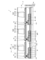
次に、表示装置1の断面構成について説明する。図7は、図2のVII-VII’断面図である。図8は、図1のVIII-VIII’断面図である。図7に示すように、発光素子3は、アレイ基板2の上に設けられる。アレイ基板2は、基板21、アノード電極23、対向電極25、接続電極26a、発熱抵抗体28(図10参照)、各種トランジスタ、各種配線及び各種絶縁膜を有する。
Next, the cross-sectional configuration of the
基板21は絶縁基板であり、例えば、石英、無アルカリガラス等のガラス基板、又はポリイミド等の樹脂基板が用いられる。基板21として、可撓性を有する樹脂基板を用いた場合には、シートディスプレイとして表示装置1を構成することができる。また、基板21は、ポリイミドに限らず、他の樹脂材料を用いても良い。
The
なお、本明細書において、基板21の表面に垂直な方向において、基板21から発光素子3に向かう方向を「上側」又は単に「上」とする。また、発光素子3から基板21に向かう方向を「下側」又は単に「下」とする。
Note that in this specification, the direction from the
基板21の上にアンダーコート膜91が設けられる。アンダーコート膜91は、例えば、絶縁膜91a、91b、91cを有する3層積層構造である。絶縁膜91aはシリコン酸化膜であり、絶縁膜91bはシリコン窒化膜であり、絶縁膜91cはシリコン酸化膜である。下層の絶縁膜91aは、基板21とアンダーコート膜91との密着性向上のために設けられる。中層の絶縁膜91bは、外部からの水分及び不純物のブロック膜として設けられる。上層の絶縁膜91cは、絶縁膜91bのシリコン窒化膜中に含有する水素原子が半導体層61側に拡散しないようにするブロック膜として設けられる。
An
アンダーコート膜91の構成は、図7に示すものに限定されない。例えば、アンダーコート膜91は、単層膜あるいは2層積層膜であってもよく、4層以上積層されていてもよい。また、基板21がガラス基板である場合、シリコン窒化膜は比較的密着性が良いため、基板21上に直接シリコン窒化膜を形成してもよい。
The structure of
遮光膜65は、絶縁膜91aの上に設けられる。遮光膜65は、半導体層61と基板21との間に設けられる。遮光膜65により、半導体層61のチャネル領域61aへの基板21側からの光の侵入を抑制することができる。あるいは、遮光膜65を導電性材料で形成して、所定の電位を与えることで、駆動トランジスタDRTへのバックゲート効果を与えることができる。なお、遮光膜65は、基板21上に設けられ、遮光膜65を覆って絶縁膜91aが設けられていてもよい。
The
駆動トランジスタDRTは、アンダーコート膜91の上に設けられる。なお、図7では、複数のトランジスタのうち、駆動トランジスタDRTを示しているが、画素回路PICAに含まれる発光制御トランジスタBCT、初期化トランジスタIST、書込トランジスタSST、リセットトランジスタRST及び発熱制御トランジスタHSTも、駆動トランジスタDRTと同様の積層構造を有する。
Drive transistor DRT is provided on
駆動トランジスタDRTは、半導体層61、ソース電極62、ドレイン電極63及びゲート電極64を有する。半導体層61は、アンダーコート膜91の上に設けられる。半導体層61は、例えば、ポリシリコンが用いられる。ただし、半導体層61は、これに限定されず、微結晶酸化物半導体、アモルファス酸化物半導体、低温ポリシリコン等であってもよい。駆動トランジスタDRTとして、n型TFTのみ示しているが、p型TFTを同時に形成しても良い。n型TFTでは、半導体層61は、チャネル領域61a、ソース領域61b、ドレイン領域61c及び低濃度不純物領域61dを有する。低濃度不純物領域61dは、チャネル領域61aとソース領域61bとの間に設けられ、また、チャネル領域61aとドレイン領域61cとの間に設けられる。
Drive transistor DRT has a
ゲート絶縁膜92は、半導体層61を覆ってアンダーコート膜91の上に設けられる。ゲート絶縁膜92は、例えばシリコン酸化膜である。ゲート電極64は、ゲート絶縁膜92の上に設けられる。また、ゲート電極64と同層に第1配線66が設けられる。ゲート電極64及び第1配線66は、例えば、モリブデンタングステン(MoW)が用いられる。図7に示す例では、駆動トランジスタDRTは、ゲート電極64が半導体層61の上側に設けられたトップゲート構造である。ただし、これに限定されず、駆動トランジスタDRTは、半導体層61の下側にゲート電極64が設けられたボトムゲート構造でもよく、半導体層61の上側及び下側の両方にゲート電極64が設けられたデュアルゲート構造でもよい。
層間絶縁膜93は、ゲート電極64を覆ってゲート絶縁膜92の上に設けられる。層間絶縁膜93は、例えば、シリコン窒化膜とシリコン酸化膜との積層構造を有する。ソース電極62及びドレイン電極63は、層間絶縁膜93の上に設けられる。ソース電極62は、ゲート絶縁膜92及び層間絶縁膜93に設けられたコンタクトホールを介して、ソース領域61bに接続される。ドレイン電極63は、ゲート絶縁膜92及び層間絶縁膜93に設けられたコンタクトホールを介して、ドレイン領域61cに接続される。ソース電極62には、引き回し配線となる第2配線67が接続される。ソース電極62、ドレイン電極63及び第2配線67は、例えば、チタン(Ti)、アルミニウム(Al)、チタン(Ti)の3層積層構造を採用することができる。
第2配線67の一部は、第1配線66と重なる領域に形成される。層間絶縁膜93を介して対向する第1配線66と第2配線67とで、保持容量Cs1が形成される。また、第1配線66は、半導体層61の一部と重なる領域に形成される。保持容量Cs1は、ゲート絶縁膜92を介して対向する半導体層61と第1配線66とで形成される容量も含む。
A portion of the
平坦化膜94は、駆動トランジスタDRT及び第2配線67を覆って層間絶縁膜93の上に設けられる。平坦化膜94としては感光性アクリル等の有機材料が用いられる。感光性アクリル等の有機材料は、CVD等により形成される無機絶縁材料に比べ、配線段差のカバレッジ性や、表面の平坦性に優れる。
The
平坦化膜94の上に、対向電極25、容量絶縁膜95、アノード電極23、アノード電極絶縁膜96の順に積層される。対向電極25は、例えばITO(Indium Tin Oxide)等の透光性を有する導電性材料で構成される。対向電極25と同層に接続電極26aが設けられる。接続電極26aは、平坦化膜94に設けられたコンタクトホールH1の内部を覆って設けられ、コンタクトホールH1の底部で第2配線67と接続される。
On the
容量絶縁膜95は、対向電極25及び接続電極26aを覆って設けられ、コンタクトホールH1と重なる領域に開口を有する。容量絶縁膜95は、例えば、シリコン窒化膜である。アノード電極23は、容量絶縁膜95を介して対向電極25と対向する。アノード電極23は、コンタクトホールH1を介して接続電極26a及び第2配線67と電気的に接続される。これにより、アノード電極23は、駆動トランジスタDRTと電気的に接続される。アノード電極23は、モリブデン(Mo)、アルミニウム(Al)の積層構造としている。ただし、これに限定されず、アノード電極23は、モリブデン、チタンの金属のいずれか1つ以上を含む材料であってもよい。又は、アノード電極23は、モリブデン、チタンのいずれか1つ以上を含む合金、又は透光性導電材料であってもよい。
Capacitive insulating
容量絶縁膜95を介して対向するアノード電極23と対向電極25との間に容量Cs2が形成される。また、ITOで形成される対向電極25は、アノード電極23を形成する工程において、第2配線67等の各種配線を保護するためのバリア膜としての機能も有する。ところで、アノード電極23のパターニング時、一部において対向電極25がエッチング環境にさらされるが、対向電極25の形成からアノード電極23の形成までの間に行われるアニール処理によって、対向電極25はアノード電極23のエッチングに対し十分な耐性を有する。
A capacitor Cs2 is formed between the
アノード電極絶縁膜96は、アノード電極23を覆って設けられる。アノード電極絶縁膜96は、例えばシリコン窒化膜である。アノード電極絶縁膜96は、アノード電極23の周縁部を覆っており、隣り合う副画素49のアノード電極23を絶縁する。
The anode
アノード電極絶縁膜96は、アノード電極23と重なる位置に、発光素子3を実装するための開口OPを有する。開口OPの大きさは、発光素子3の実装工程における実装ズレ量等を考慮し、発光素子3よりも大きい面積の開口とする。すなわち、基板21に垂直な方向からの平面視で、アノード電極23の面積は、発光素子3の面積よりも大きい。さらに、発光素子3は、少なくとも2つの端子(アノード端子33及びカソード端子32)を有し、基板21に垂直な方向からの平面視で、アノード電極23の面積は、少なくとも2つの端子(アノード端子33及びカソード端子32)の一方の面積よりも大きい。例えば発光素子3が平面視で、10μm×10μm程度の実装面積である場合、開口OPの面積として、20μm×20μm程度は確保されることが好ましい。
The anode
発光素子3R、3G、3Bは、それぞれに対応するアノード電極23に実装される。各発光素子3は、アノード端子33がアノード電極23に接するように実装される。発光素子3は、半導体層31、カソード端子32及びアノード端子33を有する。半導体層31は、n型クラッド層、活性層及びp型クラッド層が積層された構成を採用することができる。
The
半導体層31は、例えば、窒化ガリウム(GaN)、アルミニウムインジウム燐(AlInP)等の化合物半導体が用いられる。半導体層31は、発光素子3R、3G、3Bごとに異なる材料が用いられてもよい。また、活性層として、高効率化のために数原子層からなる井戸層と障壁層とを周期的に積層させた多重量子井戸構造(MQW構造)が採用されてもよい。また、発光素子3として、半導体基板上に半導体層31が形成された構成でもよい。あるいは、発光素子3単体がアレイ基板2に実装される構成に限定されず、発光素子3を含むLEDチップがアレイ基板2に実装される構成であってもよい。LEDチップは、例えば、発光素子基板と、発光素子基板に設けられた発光素子3と、発光素子基板に設けられ、発光素子3を駆動する回路素子群とを有し、発光素子基板、発光素子3及び回路素子群が1チップに集積された構成が挙げられる。
For the semiconductor layer 31, a compound semiconductor such as gallium nitride (GaN) or aluminum indium phosphorus (AlInP) is used, for example. Different materials may be used for the semiconductor layer 31 for each of the
複数の発光素子3の間に素子絶縁膜97が設けられる。素子絶縁膜97は樹脂材料で形成される。素子絶縁膜97は、発光素子3の側面を覆っており、発光素子3のカソード端子32は、素子絶縁膜97から露出する。素子絶縁膜97の上面と、カソード端子32の上面とが同一面を形成するように、素子絶縁膜97は平坦に形成される。ただし、素子絶縁膜97の上面の位置は、カソード端子32の上面の位置と異なっていてもよい。
An
カソード電極22は、複数の発光素子3及び素子絶縁膜97を覆って、複数の発光素子3に電気的に接続される。より具体的には、カソード電極22は、素子絶縁膜97の上面と、カソード端子32の上面とに亘って設けられる。カソード電極22は、例えばITO等の透光性を有する導電性材料が用いられる。これにより、発光素子3からの出射光を効率よく外部に取り出すことができる。カソード電極22は、表示領域AAに実装された複数の発光素子3のカソード端子32と電気的に接続される。
The
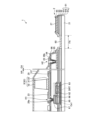
図8に示すように、カソード電極22は、表示領域AAの外側に設けられた陰極コンタクト部(コンタクトホールH2)で、アレイ基板2側に設けられたカソード配線60と接続される。なお、図6では、周辺領域GAの断面構成と、表示領域AAの断面構成との対応関係を分かりやすくするために、周辺領域GAと表示領域AAとを併せて示している。
As shown in FIG. 8, the
図8に示すように、表示装置1は、周辺領域GAにおいて、端子部27、折曲領域FA及び陰極コンタクト部(コンタクトホールH2)を有する。端子部27は、駆動IC210又はフレキシブルプリント基板等の配線基板と接続される端子である。折曲領域FAは、アレイ基板2のうち、端子部27側の周辺領域GAを折り曲げるため領域である。なお、折曲領域FAが設けられる場合には、基板21として可撓性を有する樹脂材料が用いられる。
As shown in FIG. 8, the
具体的には、アンダーコート膜91、ゲート絶縁膜92及び層間絶縁膜93は、表示領域AAから周辺領域GAに亘って、基板21の端部まで設けられている。アンダーコート膜91、ゲート絶縁膜92及び層間絶縁膜93は、折曲領域FAで除去される。アンダーコート膜91、ゲート絶縁膜92及び層間絶縁膜93は、折曲領域FAにおいて、エッチングにより除去される。この場合、ポリイミド等の樹脂材料で構成される基板21の表面が一部エッチングにより浸食されて凹部が形成される場合がある。
Specifically, the
カソード配線60は、層間絶縁膜93の上に設けられる。つまり、カソード配線60は、ソース電極62、ドレイン電極63及び第2配線67と同層に設けられ、同じ材料で形成される。カソード配線60は、折曲領域FAに跨がって設けられ、アンダーコート膜91、ゲート絶縁膜92及び層間絶縁膜93と、基板21とで形成される段差に沿って設けられる。また、カソード配線60は、折曲領域FAにおいて基板21の上に設けられ、折曲領域FAと基板21の端部との間において、層間絶縁膜93の上に設けられる。
平坦化膜94は、周辺領域GAの、折曲領域FA及び折曲領域FAと基板21の端部との間の領域で除去される。平坦化膜94には、折曲領域FAと表示領域AAとの間の領域にコンタクトホールH2が設けられる。カソード配線60はコンタクトホールH2の底面に露出する、また、素子絶縁膜97の厚さは、表示領域AAの周縁部から周辺領域GAに向かって、薄くなるように設けられる。カソード電極22は、コンタクトホールH2の内部に設けられた接続電極26bを介して、カソード配線60と電気的に接続される。接続電極26bは、対向電極25及び接続電極26aと同層に設けられ、対向電極25及び接続電極26aと同じ材料で形成される。
The
また、端子部27は、折曲領域FAと基板21の端部との間の領域で、カソード配線60の上に設けられる。容量絶縁膜95は、端子部27を覆って設けられ、端子部27と重なる領域に開口を有する。
Further, the
以上のように、表示素子として発光素子3を用いた表示装置1が構成される。なお、表示装置1は、必要に応じて、カソード電極22の上側に、カバーガラスやタッチパネル等を設けてもよい。また、この場合、表示装置1とカバーガラス等の部材との間に、樹脂などを用いた充填材が設けられていてもよい。また、表示装置1において、発光素子3の上部でカソード電極22に接続されるフェースアップ構造に限定されず、発光素子3の下部が、アノード電極23及びカソード電極22に接続される、いわゆるフェースダウン構造であってもよい。
As described above, the
次に、副画素49及び発熱抵抗体28の詳細な構成について説明する。図9は、第1実施形態に係る表示装置の、1つの副画素を拡大して示す平面図である。図10は、図9のX-X’断面図である。なお、図9では、図面を見やすくするために、発光素子3を省略して示す。また、図9では、アノード電極23を二点鎖線で示し、アノード電源線L1、映像信号線L2、リセット信号線L3、初期化信号線L4、接続配線L5、L6及び発熱抵抗体28に斜線を付けて示している。また、各トランジスタが有する半導体層61、71、76、77、78、79を点線で示している。
Next, detailed configurations of the
図9に示すように、アノード電源線L1、映像信号線L2及び初期化信号線L4は、第2方向Dyに延在する。リセット信号線L3はアノード電源線L1と映像信号線L2との間に設けられる。なお、リセット信号線L3は、図面を見やすくするために簡略化して示しているが、アノード電源線L1等と同様に第2方向Dyに延在して設けられる。 As shown in FIG. 9, the anode power line L1, the video signal line L2, and the initialization signal line L4 extend in the second direction Dy. The reset signal line L3 is provided between the anode power supply line L1 and the video signal line L2. Although the reset signal line L3 is shown in a simplified manner to make the drawing easier to read, it is provided to extend in the second direction Dy like the anode power supply line L1 and the like.
リセット制御走査線RG、発光制御走査線BG、書込制御走査線SG、初期化制御走査線IG及び発熱制御走査線HGは、それぞれ、第1方向Dxに延在し、平面視で、アノード電源線L1及び映像信号線L2とそれぞれ交差する。接続配線L5は、駆動トランジスタDRT、初期化トランジスタIST及び書込トランジスタSSTを接続する。接続配線L6は、発熱抵抗体28と、発熱制御トランジスタHSTとを接続する。
The reset control scanning line RG, the light emission control scanning line BG, the write control scanning line SG, the initialization control scanning line IG, and the heat generation control scanning line HG each extend in the first direction Dx, and in plan view, the anode power supply It intersects with the line L1 and the video signal line L2, respectively. The connection wiring L5 connects the drive transistor DRT, the initialization transistor IST, and the write transistor SST. The connection wiring L6 connects the
駆動トランジスタDRTを構成する半導体層61、ソース電極62(第2配線67)、ゲート電極64(第1配線66)は、アノード電源線L1、映像信号線L2、発光制御走査線BG及び書込制御走査線SGで囲まれた領域に設けられる。半導体層61は、ゲート電極64(第1配線66)と重ならない部分で、コンタクトホールH3を介してソース電極62(第2配線67)と接続される。アノード電極23及び対向電極25は、駆動トランジスタDRTと重なる領域に設けられる。対向電極25は、カソード電源線L10に接続され、カソード電源電位PVSSが供給される。これにより、対向電極25は、アレイ基板2の各トランジスタ及び各種配線と、アノード電極23及び発光素子3との間をシールドすることができる。
The
アノード電極23は、駆動トランジスタDRTと重ならない領域まで延在し、アノード電極23の一部が発熱抵抗体28の一端側28e1と重なる。発熱抵抗体28は、平面視でミアンダ状の配線パターンを有し、全体として、アノード電源線L1に沿って第2方向Dyに延在する。発熱抵抗体28の一端側28e1は、コンタクトホールH4を介してアノード電極23と接続される。また、発熱抵抗体28の他端側28e2は、コンタクトホールH5を介して接続配線L6と接続される。
The
発熱制御トランジスタHSTは、半導体層71、ソース電極72、ドレイン電極73及びゲート電極74を有する。半導体層71は、第2方向Dyに延在し、発熱制御走査線HGと平面視で交差する。半導体層71のうち、発熱制御走査線HGと重なる領域にチャネル領域が形成される。発熱制御走査線HGのうち半導体層71と重なる部分が、発熱制御トランジスタHSTのゲート電極74として機能する。半導体層71の一端側は、アノード電源線接続部L1bと接続される。半導体層71の他端側は、接続配線L6と接続される。アノード電源線接続部L1bは、アノード電源線L1から第1方向Dxに分岐された部分である。アノード電源線接続部L1b及び接続配線L6の一部が、それぞれソース電極72及びドレイン電極73として機能する。
Heat generation control transistor HST has a
このような構成により、発熱抵抗体28の一端側28e1がアノード電極23に電気的に接続され、発熱抵抗体28の他端側28e2が発熱制御トランジスタHSTを介してアノード電源線L1に電気的に接続される。
With this configuration, one end side 28e1 of the
発光制御トランジスタBCTは、半導体層76有する。半導体層76は駆動トランジスタDRTの半導体層61と接続されており、発光制御走査線BGと平面視で交差する。半導体層76の一端側は、アノード電源線接続部L1aと電気的に接続される。アノード電源線接続部L1aは、アノード電源線L1から第1方向Dxに分岐された部分である。これにより、駆動トランジスタDRT及び発光制御トランジスタBCTには、アノード電源線L1に電気的に接続される。
The light emission control transistor BCT has a
リセットトランジスタRSTは、半導体層77を有する。半導体層77の一端側は、リセット信号線L3と接続され、半導体層77の他端側は、駆動トランジスタDRTの半導体層61と接続される。半導体層77は、第2方向Dyに延在し、平面視で発光制御走査線BG及びリセット制御走査線RGと交差する。半導体層77の、リセット制御走査線RGと重なる部分にチャネル領域が形成される。
Reset transistor RST has a
半導体層77及び半導体層76は、半導体層61と接続されているので、図3に示す回路図に示す、駆動トランジスタDRT、発光制御トランジスタBCT及びリセットトランジスタRSTの接続構成が実現される。
Since the
書込トランジスタSSTは半導体層78を有する。半導体層78の一端側は、映像信号線接続部L2aと接続される。映像信号線接続部L2aは、映像信号線L2から第1方向Dxに分岐された部分である。半導体層78の他端側は、接続配線L5と接続される。半導体層78は、第1方向Dxに延在し、平面視で分岐部SGaと交差する。分岐部SGaは、書込制御走査線SGから第2方向Dyに分岐された部分である。
Write transistor SST has a
初期化トランジスタISTは半導体層79を有する。半導体層79の一端側は、初期化信号線L4と接続される。半導体層79の他端側は、接続配線L5と接続される。半導体層79は、第2方向Dyに延在し、平面視で初期化制御走査線IGと交差する。
Initialization transistor IST has a
図10に示すように、発熱抵抗体28は、平坦化膜94の上に設けられる。発熱抵抗体28は、対向電極25と同層に設けられ、基板21に垂直な方向において、映像信号線L2、発熱抵抗体28、アノード電極23の順に積層される。発熱抵抗体28は、対向電極25と同じ材料、すなわちITO等の透光性を有する導電性材料で構成される。発熱抵抗体28は、アノード電極23よりも高いシート抵抗値を有し、発熱抵抗体28に電流が流れた場合に、電気エネルギーが良好に熱に変換される。なお、発熱抵抗体28は、ITOに限定されず、In2O3にGe、Mo、F、Ti、Zr、Hf、Nb、Ta、W、あるいはTeをドープした透光性導電膜、ZnOにAl、Ga、B、In、Y、Sc、F、V、Si、Ge、Ti、Zr、あるいはHfをドープした透光性導電膜、SnO2にSb、F、As、Nb、あるいはTaをドープした透光性導電膜であってもよい。又は、発熱抵抗体28は、モリブデン(Mo)若しくはMo合金、タングステン(W)若しくはW合金、又はチタン(Ti)若しくはTi合金等の高融点材料で形成されてもよい。
As shown in FIG. 10, the
また、発熱抵抗体28は、容量絶縁膜95を介してアノード電極23と異なる層に設けられ、容量絶縁膜95に設けられたコンタクトホールH4を介してアノード電極23と接続される。これにより、発熱抵抗体28で発生した熱が、コンタクトホールH4及びアノード電極23を経由して発光素子3に良好に伝わる。また、アノード電極23は、発熱抵抗体28よりも、平面視での面積が大きく、熱伝導率が高い。このため、コンタクトホールH4の周囲の、アノード電極23と発熱抵抗体28との重畳部分でも、発熱抵抗体28で発生した熱がアノード電極23に伝わる。
Further, the
発熱制御トランジスタHSTの積層構造は、図7に示した駆動トランジスタDRTと同様であり、詳細な説明は省略する。ソース電極72(アノード電源線接続部L1b)及びドレイン電極73(接続配線L6)、アノード電源線L1及び映像信号線L2は、駆動トランジスタDRTのソース電極62(第2配線67)及びドレイン電極63と同層に設けられる。なお、図10では図示されないが、リセット信号線L3、初期化信号線L4及び接続配線L5もアノード電源線L1等と同層に設けられる。
The stacked structure of the heat generation control transistor HST is similar to that of the drive transistor DRT shown in FIG. 7, and detailed description thereof will be omitted. The source electrode 72 (anode power line connection portion L1b), the drain electrode 73 (connection wiring L6), the anode power line L1, and the video signal line L2 are connected to the source electrode 62 (second wiring 67) and
発熱制御走査線HG、初期化制御走査線IG及び書込制御走査線SGは、ゲート電極64(第1配線66)と同層に設けられる。なお、図10では図示されないが、発光制御走査線BG及びリセット制御走査線RGも発熱制御走査線HG等と同層に設けられる。 The heat generation control scanning line HG, the initialization control scanning line IG, and the write control scanning line SG are provided in the same layer as the gate electrode 64 (first wiring 66). Although not shown in FIG. 10, the light emission control scanning line BG and the reset control scanning line RG are also provided in the same layer as the heat generation control scanning line HG and the like.
発熱制御トランジスタHSTの半導体層71及び各トランジスタが有する半導体層76、77、78、79は、駆動トランジスタDRTの半導体層61と同層に設けられる。ただし、発熱制御トランジスタHSTの半導体層71、ソース電極72(アノード電源線接続部L1b)及びドレイン電極73及びゲート電極74は、それぞれ駆動トランジスタDRTと異なる層に設けられていてもよい。
The
図11は、第1副画素が有する第1発熱抵抗体、第2副画素が有する第2発熱抵抗体及び第3副画素が有する第3発熱抵抗体を比較して説明するための説明図である。図11に示すように、第1副画素49Rは第1発熱抵抗体28Rを有する。第2副画素49Gは第2発熱抵抗体28Gを有する。第3副画素49Bは第3発熱抵抗体28Bを有する。図11では、第1発熱抵抗体28R、第2発熱抵抗体28G及び第3発熱抵抗体28Bを模式的に並べて示している。
FIG. 11 is an explanatory diagram for comparing and explaining the first heating resistor of the first subpixel, the second heating resistor of the second subpixel, and the third heating resistor of the third subpixel. be. As shown in FIG. 11, the
第1発熱抵抗体28R、第2発熱抵抗体28G及び第3発熱抵抗体28Bは、それぞれ、複数の第1部分28aと、複数の第2部分28bとを有する。複数の第1部分28aは、それぞれ第1方向Dxに延在し、第2方向Dyに配列される。第2部分28bは、第2方向Dyに隣り合う2つの第1部分28aの同じ側の端部を接続する。複数の第1部分28aと複数の第2部分28bとが接続されてミアンダ状の配線パターンが形成される。
The
第1発熱抵抗体28R、第2発熱抵抗体28G及び第3発熱抵抗体28Bは、配線パターンの配線長が異なる。第1発熱抵抗体28R、第2発熱抵抗体28G、第3発熱抵抗体28Bの順に配線長が長い。ここで、各発熱抵抗体28の配線長は、配線パターンに沿った合計の長さである。つまり、各発熱抵抗体28の配線長は、複数の第1部分28aの配線長W1と、複数の第2部分28bの配線長W2との合計の長さである。
The
これにより、第1発熱抵抗体28R、第2発熱抵抗体28G及び第3発熱抵抗体28Bは、異なる抵抗値を有する。具体的には、第1発熱抵抗体28Rの抵抗値は、第2発熱抵抗体28Gの抵抗値及び第3発熱抵抗体28Bの抵抗値よりも小さい。また、第2発熱抵抗体28Gの抵抗値は、第3発熱抵抗体28Bの抵抗値よりも小さい。
As a result, the
これにより、第1発熱抵抗体28Rに流れる電流が、第2発熱抵抗体28G及び第3発熱抵抗体28Bよりも大きくなり、第1発熱抵抗体28Rの発熱量が大きくなる。これにより、各副画素49が有する発光素子3Rの発光効率が、発光素子3G、発光素子3Bよりも小さい場合であっても、第1発熱抵抗体28Rにより発光素子3Rを良好に加熱することで、発光素子3Rを安定して発光させることができる。
As a result, the current flowing through the
なお、図11では、第1発熱抵抗体28R、第2発熱抵抗体28G及び第3発熱抵抗体28Bの第2方向Dyの長さを異ならせる例を示したが、他の構成で抵抗値を異ならせてもよい。例えば、第2方向Dyの長さ、つまり第1部分28a及び第2部分28bの配線長W1、W2を異ならせてもよく、第1部分28a及び第2部分28bのそれぞれの配線幅を異ならせてもよい。あるいは、第1発熱抵抗体28R、第2発熱抵抗体28G及び第3発熱抵抗体28Bとしてそれぞれ異なる材料を用いてもよい。
Although FIG. 11 shows an example in which the lengths in the second direction Dy of the
なお、図11に示した各発熱抵抗体28の配線パターンはあくまで一例であり、異なる配線パターンであってもよい。第1発熱抵抗体28R、第2発熱抵抗体28G及び第3発熱抵抗体28Bは、同じ配線パターンで形成され、同じ抵抗値を有していてもよい。また、第1副画素49R、第2副画素49G及び第3副画素49Bの全てが、発熱抵抗体28を有する構成に限定されない。少なくとも第1副画素49Rが第1発熱抵抗体28Rを有し、第2副画素49G及び第3副画素49Bの少なくとも一方が発熱抵抗体28を有さない構成を採用することもできる。
Note that the wiring pattern of each
(第2実施形態)
図12は、第2実施形態に係る画素回路を示す回路図である。なお、以下の説明においては、上述した実施形態で説明したものと同じ構成要素には同一の符号を付して重複する説明は省略する。
(Second embodiment)
FIG. 12 is a circuit diagram showing a pixel circuit according to the second embodiment. In the following description, the same components as those described in the embodiments described above are denoted by the same reference numerals, and redundant description will be omitted.
図12に示すように、第2実施形態に係る画素回路PICAは、第1実施形態に比べて、抵抗体信号線L7を有する構成が異なる。抵抗体信号線L7には、駆動IC210から、抵抗体駆動信号Vprehtが供給される。発熱抵抗体28の他端側28e2は、発熱制御トランジスタHSTを介して抵抗体信号線L7に接続される。発熱抵抗体28の一端側28e1は、第1実施形態と同様にアノード電極23に接続される。
As shown in FIG. 12, the pixel circuit PICA according to the second embodiment has a different configuration from the first embodiment in that it includes a resistor signal line L7. A resistor drive signal Vpreht is supplied from the
各トランジスタの動作は、図5に示すプレヒート期間PHと同様であり、発熱制御トランジスタHST及びリセットトランジスタRSTがオンになり、その他のトランジスタがオフになる。これにより、抵抗体信号線L7、発熱制御トランジスタHST、発熱抵抗体28、リセットトランジスタRST及びリセット信号線L3が導通して電流経路が形成される。発熱抵抗体28には、抵抗体信号線L7から供給される抵抗体駆動信号Vprehtに応じて電流が流れる。
The operation of each transistor is similar to the preheat period PH shown in FIG. 5, with the heat generation control transistor HST and reset transistor RST turned on, and the other transistors turned off. As a result, the resistor signal line L7, heat generation control transistor HST,
本実施形態では、発熱抵抗体28に供給される電位が、アノード電源線L1(アノード電源電位PVDD)から独立して制御される。このため、表示装置1の表示期間に、発熱抵抗体28の発熱を制御することも可能である。
In this embodiment, the potential supplied to the
(第3実施形態)
図13は、第3実施形態に係る画素回路を示す回路図である。図13に示すように、第3実施形態に係る画素回路PICAは、第1実施形態に比べて、発熱抵抗体28の一端側28e1が、カソード電極22に電気的に接続される構成が異なる。発熱抵抗体28の他端側28e2は、第1実施形態と同様に、発熱制御トランジスタHSTを介してアノード電源線L1に電気的に接続される。
(Third embodiment)
FIG. 13 is a circuit diagram showing a pixel circuit according to the third embodiment. As shown in FIG. 13, the pixel circuit PICA according to the third embodiment differs from the first embodiment in that one end side 28e1 of the
第3実施形態では、図5に示すプレヒート期間PHにおいて、発熱制御トランジスタHSTがオンになり、その他のトランジスタがオフになる。これにより、アノード電源線L1、発熱制御トランジスタHST、発熱抵抗体28及びカソード電源線L10が導通して電流経路が形成される。発熱抵抗体28には、アノード電源線L1(アノード電源電位PVDD)から電流が流れる。
In the third embodiment, during the preheat period PH shown in FIG. 5, the heat generation control transistor HST is turned on and the other transistors are turned off. As a result, the anode power supply line L1, heat generation control transistor HST,
第3実施形態では、プレヒート期間PHにおいて、発熱制御トランジスタHSTのオン、オフの切り換えのみで発熱抵抗体28の発熱が制御できるので、プレヒート期間PHでの画素回路PICAの駆動を簡易にできる。なお、第3実施形態では、発熱抵抗体28の一端側28e1がアノード電極23に接続されていない。この場合であっても、図9及び図10と同様に、アノード電極23の一部が発熱抵抗体28と重なって設けられる構成とすることで、発熱抵抗体28で発生した熱を、アノード電極23に効率よく伝えることができる。
In the third embodiment, the heat generation of the
なお、本実施形態の構成は第2実施形態にも適用できる。すなわち、図12に示す画素回路PICAにおいて、抵抗体信号線L7、発熱制御トランジスタHST、発熱抵抗体28及びカソード電源線L10が導通して電流経路が形成される構成も採用できる。
Note that the configuration of this embodiment can also be applied to the second embodiment. That is, in the pixel circuit PICA shown in FIG. 12, a configuration can also be adopted in which the resistor signal line L7, heat generation control transistor HST,
(第4実施形態)
図14は、第4実施形態に係る、温度センサを有する画素を示す平面図である。図15は、温度センサの一例を説明するための説明図である。図14に示すように、表示装置1Aは、画素Pixに温度センサ8及び温度センサ回路81を有する。温度センサ8は、例えばpn接合ダイオードを用いることができる。温度センサ回路81は、温度センサ8を駆動するための回路である。温度センサ回路81は、複数のトランジスタ等の回路素子を備え、温度センサ8への駆動信号の供給を制御する。
(Fourth embodiment)
FIG. 14 is a plan view showing a pixel including a temperature sensor according to the fourth embodiment. FIG. 15 is an explanatory diagram for explaining an example of a temperature sensor. As shown in FIG. 14, the
図15に示すように、温度センサ8は、センサアノード電源線SL1及びセンサカソード電源線SL10に接続され、センサアノード電源線SL1及びセンサカソード電源線SL10から順バイアス電圧信号が印加される。温度センサ回路81は、温度センサ8に一定の順方向電流Ifが流れるように制御する。
As shown in FIG. 15,
検出回路211は、温度センサ8から、出力信号としてアノードとカソードとの間の出力電圧Vfを受け取る。検出回路211は、駆動IC210に設けられていてもよいし、駆動IC210とは別のICとして設けられていてもよい。検出回路211は、pn接合ダイオードの出力電圧Vfの温度依存性に基づいて画素Pixの温度を検出することができる。駆動IC210は、画素Pixの温度の情報に基づいて、プレヒート期間PHにおいて、発熱抵抗体28に流れる電流値又は発熱制御トランジスタHSTのオン時間を適切に制御することができる。
The
なお、温度センサ回路81は、温度センサ8に一定の逆バイアス電圧信号を印加してもよい。検出回路211は、温度センサ8の出力信号として逆バイアス電流値を受け取って、逆バイアス電流値の温度依存性に基づいて温度を検出してもよい。また、温度センサ8は、各画素Pixに設けられていてもよいし、複数の画素Pixに対して1つの温度センサ8が設けられていてもよい。また、温度センサ8は各副画素49の画素回路PICAに設けられていてもよい。この場合、温度センサ8は、画素回路PICAに設けられたトランジスタの一部をセンサとして共用してもよい。又は、温度センサ8は、発光素子3を逆バイアス駆動することでセンサとして共用してもよい。
Note that the
これまでの説明において、アノード端子33、カソード端子32として表記してきた部分においては、発光素子3の接続方向、及び電圧の印加方向によっては明細書中の記載に限定するものではなく、逆転していても良い。また、図7、図8においては、発光素子3の一方の電極が下側に、他方の電極が上側にある構成を示しているが、その両方が下側、つまりアレイ基板2に対面する側に有る構成であっても良い。
In the explanation so far, the parts described as the
以上、本発明の好適な実施の形態を説明したが、本発明はこのような実施の形態に限定されるものではない。実施の形態で開示された内容はあくまで一例にすぎず、本発明の趣旨を逸脱しない範囲で種々の変更が可能である。本発明の趣旨を逸脱しない範囲で行われた適宜の変更についても、当然に本発明の技術的範囲に属する。上述した各実施形態及び各変形例の要旨を逸脱しない範囲で、構成要素の種々の省略、置換及び変更のうち少なくとも1つを行うことができる。 Although preferred embodiments of the present invention have been described above, the present invention is not limited to such embodiments. The contents disclosed in the embodiments are merely examples, and various changes can be made without departing from the spirit of the present invention. Appropriate changes made without departing from the spirit of the present invention also naturally fall within the technical scope of the present invention. At least one of various omissions, substitutions, and modifications of the constituent elements can be made without departing from the gist of each of the embodiments and modifications described above.
1、1A 表示装置
2 アレイ基板
3、3R、3G、3B 発光素子
8 温度センサ
12 駆動回路
21 基板
22 カソード電極
23 アノード電極
27 端子部
28 発熱抵抗体
28R 第1発熱抵抗体
28G 第2発熱抵抗体
28B 第3発熱抵抗体
28e1 一端側
28e2 他端側
31 半導体層
32 カソード端子
33 アノード端子
49 副画素
60 カソード配線
210 駆動IC
DRT 駆動トランジスタ
BCT 発光制御トランジスタ
IST 初期化トランジスタ
SST 書込トランジスタ
RST リセットトランジスタ
HST 発熱制御トランジスタ
BG 発光制御走査線
HG 発熱制御走査線
IG 初期化制御走査線
RG リセット制御走査線
SG 書込制御走査線
L1 アノード電源線
L10 カソード電源線
Pix 画素
PICA 画素回路
1,
DRT Drive transistor BCT Light emission control transistor IST Initialization transistor SST Write transistor RST Reset transistor HST Heat generation control transistor BG Light emission control scan line HG Heat generation control scan line IG Initialization control scan line RG Reset control scan line SG Write control scan line L1 Anode power line L10 Cathode power line Pix Pixel PICA Pixel circuit
Claims (11)
前記基板に設けられた複数の画素と、
複数の前記画素の各々に設けられる発光素子と、
前記基板に設けられ、前記発光素子と電気的に接続される第1電極と、
前記第1電極と電気的に接続されるトランジスタと、
前記基板に設けられ、前記発光素子に駆動信号を供給する画素回路と、
前記画素回路に設けられた発熱抵抗体と、を有し、
前記発熱抵抗体は、前記第1電極よりも高いシート抵抗値を有し、
前記基板に垂直な方向からの平面視で、前記発熱抵抗体はミアンダ状の配線パターンを有し、
前記複数の画素の一は、赤色の赤色を表示する第1副画素と、緑色を表示する第2副画素と、青色を表示する第3副画素とを含み、
前記第1副画素は、前記発熱抵抗体として第1発熱抵抗体を有し、
前記第2副画素は、前記発熱抵抗体として第2発熱抵抗体を有し、
前記第3副画素は、前記発熱抵抗体として第3発熱抵抗体を有し、
前記第1副画素が有する前記第1発熱抵抗体の抵抗値は、前記第2発熱抵抗体の抵抗値及び前記第3発熱抵抗体の抵抗値よりも小さい
表示装置。 A substrate and
a plurality of pixels provided on the substrate;
a light emitting element provided in each of the plurality of pixels;
a first electrode provided on the substrate and electrically connected to the light emitting element;
a transistor electrically connected to the first electrode;
a pixel circuit provided on the substrate and supplying a drive signal to the light emitting element;
a heating resistor provided in the pixel circuit;
The heating resistor has a sheet resistance value higher than that of the first electrode,
When viewed from above in a direction perpendicular to the substrate, the heating resistor has a meandering wiring pattern,
One of the plurality of pixels includes a first sub-pixel that displays red, a second sub-pixel that displays green, and a third sub-pixel that displays blue,
The first sub-pixel has a first heating resistor as the heating resistor,
The second sub-pixel has a second heating resistor as the heating resistor,
The third sub-pixel has a third heating resistor as the heating resistor,
The resistance value of the first heating resistor of the first sub-pixel is smaller than the resistance value of the second heating resistor and the resistance value of the third heating resistor.
Display device.
請求項1に記載の表示装置。 The display device according to claim 1, wherein one end side of the heating resistor is electrically connected to the first electrode.
前記第2電極を介して、第2電位を前記発光素子に供給する第2電源線と、を有し、
前記発熱抵抗体の一端側は前記第2電極に電気的に接続される
請求項1に記載の表示装置。 a second electrode provided on the substrate and electrically connected to the light emitting element;
a second power supply line that supplies a second potential to the light emitting element via the second electrode;
The display device according to claim 1, wherein one end side of the heating resistor is electrically connected to the second electrode.
前記発熱抵抗体の他端側は前記第1電源線に電気的に接続される
請求項2又は請求項3に記載の表示装置。 The pixel circuit has a first power line that supplies a first potential to the light emitting element via the first electrode,
The display device according to claim 2 or 3, wherein the other end side of the heating resistor is electrically connected to the first power supply line.
前記発熱抵抗体の他端側は前記抵抗体信号線に電気的に接続される
請求項2又は請求項3に記載の表示装置。 The pixel circuit has a resistor signal line that supplies a resistor drive signal to the heat generating resistor,
The display device according to claim 2 or 3, wherein the other end of the heating resistor is electrically connected to the resistor signal line.
請求項1から請求項5のいずれか1項に記載の表示装置。 The display device according to any one of claims 1 to 5, wherein at least a portion of the first electrode is provided to overlap with the heating resistor when viewed in plan from a direction perpendicular to the substrate.
前記第2電極は、複数の前記発光素子及び前記素子絶縁膜を覆って、複数の前記発光素子に電気的に接続される
請求項3に記載の表示装置。 an element insulating film provided between the plurality of light emitting elements and covering at least part of the side surfaces of the plurality of light emitting elements;
The display device according to claim 3, wherein the second electrode covers the plurality of light emitting elements and the element insulating film and is electrically connected to the plurality of light emitting elements.
請求項1から請求項7のいずれか1項に記載の表示装置。 The heating resistor is provided in a layer different from the first electrode through an insulating film, and is connected to the first electrode through a contact hole provided in the insulating film. The display device according to any one of the items.
前記基板に垂直な方向において、前記信号線、前記発熱抵抗体、前記第1電極の順に積層される
請求項1から請求項8のいずれか1項に記載の表示装置。 further comprising a signal line that supplies a video signal to the transistor,
The display device according to any one of claims 1 to 8, wherein the signal line, the heating resistor, and the first electrode are stacked in this order in a direction perpendicular to the substrate.
前記温度センサからの出力信号を受け取って、前記出力信号の温度依存性に基づいて温度を検出する検出回路と、を有する
請求項1から請求項9のいずれか1項に記載の表示装置。 a temperature sensor provided in the pixel;
The display device according to any one of claims 1 to 9 , further comprising a detection circuit that receives an output signal from the temperature sensor and detects temperature based on temperature dependence of the output signal.
請求項1から請求項10のいずれか1項に記載の表示装置。 The display device according to any one of claims 1 to 10 , wherein the heating resistor is provided in a layer above the transistor and below the first electrode.
Priority Applications (4)
| Application Number | Priority Date | Filing Date | Title |
|---|---|---|---|
| JP2019047597A JP7360246B2 (en) | 2019-03-14 | 2019-03-14 | display device |
| PCT/JP2019/050422 WO2020183861A1 (en) | 2019-03-14 | 2019-12-23 | Display device |
| TW109107779A TWI738242B (en) | 2019-03-14 | 2020-03-10 | Display device |
| US17/471,202 US11721276B2 (en) | 2019-03-14 | 2021-09-10 | Display device |
Applications Claiming Priority (1)
| Application Number | Priority Date | Filing Date | Title |
|---|---|---|---|
| JP2019047597A JP7360246B2 (en) | 2019-03-14 | 2019-03-14 | display device |
Publications (3)
| Publication Number | Publication Date |
|---|---|
| JP2020148964A JP2020148964A (en) | 2020-09-17 |
| JP2020148964A5 JP2020148964A5 (en) | 2022-03-22 |
| JP7360246B2 true JP7360246B2 (en) | 2023-10-12 |
Family
ID=72427423
Family Applications (1)
| Application Number | Title | Priority Date | Filing Date |
|---|---|---|---|
| JP2019047597A Active JP7360246B2 (en) | 2019-03-14 | 2019-03-14 | display device |
Country Status (4)
| Country | Link |
|---|---|
| US (1) | US11721276B2 (en) |
| JP (1) | JP7360246B2 (en) |
| TW (1) | TWI738242B (en) |
| WO (1) | WO2020183861A1 (en) |
Families Citing this family (8)
| Publication number | Priority date | Publication date | Assignee | Title |
|---|---|---|---|---|
| KR102952466B1 (en) | 2020-10-30 | 2026-04-15 | 미쿠니 일렉트론 코포레이션 | Display devices equipped with touch and fingerprint sensors |
| KR102810624B1 (en) * | 2021-02-23 | 2025-05-22 | 삼성디스플레이 주식회사 | Pixel circuit, display apparatus including the same and method of driving the same |
| CN113870791B (en) * | 2021-10-11 | 2023-07-25 | 京东方科技集团股份有限公司 | Pixel driving circuit and driving method thereof |
| KR20230095457A (en) * | 2021-12-22 | 2023-06-29 | 엘지디스플레이 주식회사 | Organic Light Emitting Diode Display Device Including Low Level Line |
| US11961822B2 (en) * | 2022-01-17 | 2024-04-16 | Samsung Display Co., Ltd. | Display device, and tiled display device including the display device |
| CN114882816B (en) * | 2022-06-16 | 2025-01-14 | 厦门天马微电子有限公司 | Display panel and detection method thereof, and display device |
| JP2024171113A (en) * | 2023-05-29 | 2024-12-11 | 株式会社ジャパンディスプレイ | Temperature control method for electronic device and electronic device |
| KR20250071980A (en) * | 2023-11-15 | 2025-05-23 | 엘지디스플레이 주식회사 | Display device and method for fabricating the same |
Citations (6)
| Publication number | Priority date | Publication date | Assignee | Title |
|---|---|---|---|---|
| JP2002307734A (en) | 2001-03-29 | 2002-10-23 | Shandong Hualing Electronics Co Ltd | Thermal printer head and its manufacturing method |
| JP2005309731A (en) | 2004-04-21 | 2005-11-04 | Toppan Printing Co Ltd | Board design apparatus, board design method, and board design program |
| JP2005321684A (en) | 2004-05-11 | 2005-11-17 | Sony Corp | Video display device and video display method |
| US20050258446A1 (en) | 2004-05-18 | 2005-11-24 | New Millennium Media International Inc. | LED assembly with vented circuit board |
| JP2007081094A (en) | 2005-09-14 | 2007-03-29 | Seiko Epson Corp | LIGHT EMITTING DEVICE AND ELECTRONIC DEVICE |
| JP2014082383A (en) | 2012-10-17 | 2014-05-08 | Kyocera Corp | Light-emitting unit, light-emission control unit, and light-emitting device |
Family Cites Families (15)
| Publication number | Priority date | Publication date | Assignee | Title |
|---|---|---|---|---|
| US6879110B2 (en) * | 2000-07-27 | 2005-04-12 | Semiconductor Energy Laboratory Co., Ltd. | Method of driving display device |
| JP4452076B2 (en) * | 2001-09-07 | 2010-04-21 | パナソニック株式会社 | EL display device. |
| US6911624B2 (en) * | 2002-08-23 | 2005-06-28 | Micron Technology, Inc. | Component installation, removal, and replacement apparatus and method |
| JP2012231083A (en) * | 2011-04-27 | 2012-11-22 | Hitachi Consumer Electronics Co Ltd | Back light and liquid crystal display unit using the same |
| JP6152801B2 (en) * | 2014-01-21 | 2017-06-28 | 豊田合成株式会社 | Light emitting device and manufacturing method thereof |
| JP2015215780A (en) * | 2014-05-12 | 2015-12-03 | 株式会社ジャパンディスプレイ | Display device |
| GB201413578D0 (en) | 2014-07-31 | 2014-09-17 | Infiniled Ltd | A colour iled display on silicon |
| US9728125B2 (en) * | 2014-12-22 | 2017-08-08 | Shenzhen China Star Optoelectronics Technology Co., Ltd | AMOLED pixel circuit |
| KR102601579B1 (en) * | 2015-12-16 | 2023-11-13 | 삼성전자주식회사 | Substrate and light emitting device package using the same |
| CN106652877B (en) * | 2017-02-09 | 2020-02-14 | 京东方科技集团股份有限公司 | Display panel and display device |
| JP2019061929A (en) * | 2017-09-28 | 2019-04-18 | シャープ株式会社 | Illuminating device and display device provided with the same |
| CN107452345B (en) * | 2017-09-29 | 2020-01-10 | 京东方科技集团股份有限公司 | Display device brightness compensation method and device and display device |
| CN110136622B (en) * | 2018-02-02 | 2022-09-23 | 上海和辉光电股份有限公司 | Display panel, display device, and display data processing method and device |
| CN108649026A (en) * | 2018-07-06 | 2018-10-12 | 易美芯光(北京)科技有限公司 | A kind of color temperature-tunable LED structure |
| CN109360525A (en) * | 2018-09-13 | 2019-02-19 | 天长市辉盛电子有限公司 | The control method and LED display screen system of LED display screen system |
-
2019
- 2019-03-14 JP JP2019047597A patent/JP7360246B2/en active Active
- 2019-12-23 WO PCT/JP2019/050422 patent/WO2020183861A1/en not_active Ceased
-
2020
- 2020-03-10 TW TW109107779A patent/TWI738242B/en active
-
2021
- 2021-09-10 US US17/471,202 patent/US11721276B2/en active Active
Patent Citations (6)
| Publication number | Priority date | Publication date | Assignee | Title |
|---|---|---|---|---|
| JP2002307734A (en) | 2001-03-29 | 2002-10-23 | Shandong Hualing Electronics Co Ltd | Thermal printer head and its manufacturing method |
| JP2005309731A (en) | 2004-04-21 | 2005-11-04 | Toppan Printing Co Ltd | Board design apparatus, board design method, and board design program |
| JP2005321684A (en) | 2004-05-11 | 2005-11-17 | Sony Corp | Video display device and video display method |
| US20050258446A1 (en) | 2004-05-18 | 2005-11-24 | New Millennium Media International Inc. | LED assembly with vented circuit board |
| JP2007081094A (en) | 2005-09-14 | 2007-03-29 | Seiko Epson Corp | LIGHT EMITTING DEVICE AND ELECTRONIC DEVICE |
| JP2014082383A (en) | 2012-10-17 | 2014-05-08 | Kyocera Corp | Light-emitting unit, light-emission control unit, and light-emitting device |
Also Published As
| Publication number | Publication date |
|---|---|
| WO2020183861A1 (en) | 2020-09-17 |
| JP2020148964A (en) | 2020-09-17 |
| US11721276B2 (en) | 2023-08-08 |
| TWI738242B (en) | 2021-09-01 |
| US20210407385A1 (en) | 2021-12-30 |
| TW202040548A (en) | 2020-11-01 |
Similar Documents
| Publication | Publication Date | Title |
|---|---|---|
| JP7360246B2 (en) | display device | |
| TWI715052B (en) | Display device | |
| US11410595B2 (en) | Display device and driving method for display device | |
| TWI756731B (en) | display device | |
| CN111326673B (en) | Display device | |
| WO2020189047A1 (en) | Display device | |
| CN108511485A (en) | Display device | |
| KR20150019129A (en) | Display device | |
| KR20200138543A (en) | Display device and manufacturing method thereof | |
| US12142714B2 (en) | Display device | |
| US20250096216A1 (en) | Display device | |
| WO2020084898A1 (en) | Display device | |
| US11508292B2 (en) | Display device | |
| US12588347B2 (en) | Display device | |
| JP7264669B2 (en) | Display device | |
| CN115621398B (en) | Display device | |
| US20230387374A1 (en) | Display device | |
| KR102292516B1 (en) | Display device |
Legal Events
| Date | Code | Title | Description |
|---|---|---|---|
| A521 | Request for written amendment filed |
Free format text: JAPANESE INTERMEDIATE CODE: A523 Effective date: 20220311 |
|
| A621 | Written request for application examination |
Free format text: JAPANESE INTERMEDIATE CODE: A621 Effective date: 20220311 |
|
| A131 | Notification of reasons for refusal |
Free format text: JAPANESE INTERMEDIATE CODE: A131 Effective date: 20230411 |
|
| A521 | Request for written amendment filed |
Free format text: JAPANESE INTERMEDIATE CODE: A523 Effective date: 20230612 |
|
| TRDD | Decision of grant or rejection written | ||
| A01 | Written decision to grant a patent or to grant a registration (utility model) |
Free format text: JAPANESE INTERMEDIATE CODE: A01 Effective date: 20230905 |
|
| A61 | First payment of annual fees (during grant procedure) |
Free format text: JAPANESE INTERMEDIATE CODE: A61 Effective date: 20230929 |
|
| R150 | Certificate of patent or registration of utility model |
Ref document number: 7360246 Country of ref document: JP Free format text: JAPANESE INTERMEDIATE CODE: R150 |