JP7369953B2 - スイッチング回路 - Google Patents
スイッチング回路 Download PDFInfo
- Publication number
- JP7369953B2 JP7369953B2 JP2020502843A JP2020502843A JP7369953B2 JP 7369953 B2 JP7369953 B2 JP 7369953B2 JP 2020502843 A JP2020502843 A JP 2020502843A JP 2020502843 A JP2020502843 A JP 2020502843A JP 7369953 B2 JP7369953 B2 JP 7369953B2
- Authority
- JP
- Japan
- Prior art keywords
- terminal
- gate
- switching element
- switching
- source
- Prior art date
- Legal status (The legal status is an assumption and is not a legal conclusion. Google has not performed a legal analysis and makes no representation as to the accuracy of the status listed.)
- Active
Links
Images




Classifications
-
- H—ELECTRICITY
- H03—ELECTRONIC CIRCUITRY
- H03K—PULSE TECHNIQUE
- H03K17/00—Electronic switching or gating, i.e. not by contact-making and –breaking
- H03K17/08—Modifications for protecting switching circuit against overcurrent or overvoltage
- H03K17/081—Modifications for protecting switching circuit against overcurrent or overvoltage without feedback from the output circuit to the control circuit
- H03K17/0812—Modifications for protecting switching circuit against overcurrent or overvoltage without feedback from the output circuit to the control circuit by measures taken in the control circuit
- H03K17/08122—Modifications for protecting switching circuit against overcurrent or overvoltage without feedback from the output circuit to the control circuit by measures taken in the control circuit in field-effect transistor switches
-
- H—ELECTRICITY
- H03—ELECTRONIC CIRCUITRY
- H03K—PULSE TECHNIQUE
- H03K17/00—Electronic switching or gating, i.e. not by contact-making and –breaking
- H03K17/10—Modifications for increasing the maximum permissible switched voltage
- H03K17/102—Modifications for increasing the maximum permissible switched voltage in field-effect transistor switches
-
- H—ELECTRICITY
- H03—ELECTRONIC CIRCUITRY
- H03K—PULSE TECHNIQUE
- H03K17/00—Electronic switching or gating, i.e. not by contact-making and –breaking
- H03K17/51—Electronic switching or gating, i.e. not by contact-making and –breaking characterised by the components used
- H03K17/56—Electronic switching or gating, i.e. not by contact-making and –breaking characterised by the components used by the use, as active elements, of semiconductor devices
- H03K17/687—Electronic switching or gating, i.e. not by contact-making and –breaking characterised by the components used by the use, as active elements, of semiconductor devices the devices being field-effect transistors
-
- H—ELECTRICITY
- H02—GENERATION; CONVERSION OR DISTRIBUTION OF ELECTRIC POWER
- H02M—APPARATUS FOR CONVERSION BETWEEN AC AND AC, BETWEEN AC AND DC, OR BETWEEN DC AND DC, AND FOR USE WITH MAINS OR SIMILAR POWER SUPPLY SYSTEMS; CONVERSION OF DC OR AC INPUT POWER INTO SURGE OUTPUT POWER; CONTROL OR REGULATION THEREOF
- H02M1/00—Details of apparatus for conversion
- H02M1/08—Circuits specially adapted for the generation of control voltages for semiconductor devices incorporated in static converters
-
- H—ELECTRICITY
- H02—GENERATION; CONVERSION OR DISTRIBUTION OF ELECTRIC POWER
- H02M—APPARATUS FOR CONVERSION BETWEEN AC AND AC, BETWEEN AC AND DC, OR BETWEEN DC AND DC, AND FOR USE WITH MAINS OR SIMILAR POWER SUPPLY SYSTEMS; CONVERSION OF DC OR AC INPUT POWER INTO SURGE OUTPUT POWER; CONTROL OR REGULATION THEREOF
- H02M1/00—Details of apparatus for conversion
- H02M1/32—Means for protecting converters other than automatic disconnection
- H02M1/34—Snubber circuits
-
- H—ELECTRICITY
- H03—ELECTRONIC CIRCUITRY
- H03K—PULSE TECHNIQUE
- H03K17/00—Electronic switching or gating, i.e. not by contact-making and –breaking
- H03K17/04—Modifications for accelerating switching
- H03K17/041—Modifications for accelerating switching without feedback from the output circuit to the control circuit
- H03K17/04106—Modifications for accelerating switching without feedback from the output circuit to the control circuit in field-effect transistor switches
-
- H—ELECTRICITY
- H03—ELECTRONIC CIRCUITRY
- H03K—PULSE TECHNIQUE
- H03K17/00—Electronic switching or gating, i.e. not by contact-making and –breaking
- H03K17/04—Modifications for accelerating switching
- H03K17/041—Modifications for accelerating switching without feedback from the output circuit to the control circuit
- H03K17/0412—Modifications for accelerating switching without feedback from the output circuit to the control circuit by measures taken in the control circuit
-
- H—ELECTRICITY
- H03—ELECTRONIC CIRCUITRY
- H03K—PULSE TECHNIQUE
- H03K17/00—Electronic switching or gating, i.e. not by contact-making and –breaking
- H03K17/04—Modifications for accelerating switching
- H03K17/041—Modifications for accelerating switching without feedback from the output circuit to the control circuit
- H03K17/0412—Modifications for accelerating switching without feedback from the output circuit to the control circuit by measures taken in the control circuit
- H03K17/04123—Modifications for accelerating switching without feedback from the output circuit to the control circuit by measures taken in the control circuit in field-effect transistor switches
-
- H—ELECTRICITY
- H03—ELECTRONIC CIRCUITRY
- H03K—PULSE TECHNIQUE
- H03K17/00—Electronic switching or gating, i.e. not by contact-making and –breaking
- H03K17/51—Electronic switching or gating, i.e. not by contact-making and –breaking characterised by the components used
- H03K17/56—Electronic switching or gating, i.e. not by contact-making and –breaking characterised by the components used by the use, as active elements, of semiconductor devices
- H03K17/687—Electronic switching or gating, i.e. not by contact-making and –breaking characterised by the components used by the use, as active elements, of semiconductor devices the devices being field-effect transistors
- H03K17/6877—Electronic switching or gating, i.e. not by contact-making and –breaking characterised by the components used by the use, as active elements, of semiconductor devices the devices being field-effect transistors the control circuit comprising active elements different from those used in the output circuit
-
- H—ELECTRICITY
- H03—ELECTRONIC CIRCUITRY
- H03K—PULSE TECHNIQUE
- H03K17/00—Electronic switching or gating, i.e. not by contact-making and –breaking
- H03K17/51—Electronic switching or gating, i.e. not by contact-making and –breaking characterised by the components used
- H03K17/74—Electronic switching or gating, i.e. not by contact-making and –breaking characterised by the components used by the use, as active elements, of diodes
-
- H—ELECTRICITY
- H02—GENERATION; CONVERSION OR DISTRIBUTION OF ELECTRIC POWER
- H02M—APPARATUS FOR CONVERSION BETWEEN AC AND AC, BETWEEN AC AND DC, OR BETWEEN DC AND DC, AND FOR USE WITH MAINS OR SIMILAR POWER SUPPLY SYSTEMS; CONVERSION OF DC OR AC INPUT POWER INTO SURGE OUTPUT POWER; CONTROL OR REGULATION THEREOF
- H02M7/00—Conversion of AC power input into DC power output; Conversion of DC power input into AC power output
- H02M7/003—Constructional details, e.g. physical layout, assembly, wiring or busbar connections
-
- H—ELECTRICITY
- H02—GENERATION; CONVERSION OR DISTRIBUTION OF ELECTRIC POWER
- H02M—APPARATUS FOR CONVERSION BETWEEN AC AND AC, BETWEEN AC AND DC, OR BETWEEN DC AND DC, AND FOR USE WITH MAINS OR SIMILAR POWER SUPPLY SYSTEMS; CONVERSION OF DC OR AC INPUT POWER INTO SURGE OUTPUT POWER; CONTROL OR REGULATION THEREOF
- H02M7/00—Conversion of AC power input into DC power output; Conversion of DC power input into AC power output
- H02M7/42—Conversion of DC power input into AC power output without possibility of reversal
- H02M7/44—Conversion of DC power input into AC power output without possibility of reversal by static converters
- H02M7/48—Conversion of DC power input into AC power output without possibility of reversal by static converters using discharge tubes with control electrode or semiconductor devices with control electrode
- H02M7/53—Conversion of DC power input into AC power output without possibility of reversal by static converters using discharge tubes with control electrode or semiconductor devices with control electrode using devices of a triode or transistor type requiring continuous application of a control signal
- H02M7/537—Conversion of DC power input into AC power output without possibility of reversal by static converters using discharge tubes with control electrode or semiconductor devices with control electrode using devices of a triode or transistor type requiring continuous application of a control signal using semiconductor devices only, e.g. single switched pulse inverters
- H02M7/538—Conversion of DC power input into AC power output without possibility of reversal by static converters using discharge tubes with control electrode or semiconductor devices with control electrode using devices of a triode or transistor type requiring continuous application of a control signal using semiconductor devices only, e.g. single switched pulse inverters in a push-pull configuration
-
- H—ELECTRICITY
- H03—ELECTRONIC CIRCUITRY
- H03K—PULSE TECHNIQUE
- H03K2217/00—Indexing scheme related to electronic switching or gating, i.e. not by contact-making or -breaking covered by H03K17/00
- H03K2217/0036—Means reducing energy consumption
-
- H—ELECTRICITY
- H03—ELECTRONIC CIRCUITRY
- H03K—PULSE TECHNIQUE
- H03K2217/00—Indexing scheme related to electronic switching or gating, i.e. not by contact-making or -breaking covered by H03K17/00
- H03K2217/0054—Gating switches, e.g. pass gates
-
- H—ELECTRICITY
- H03—ELECTRONIC CIRCUITRY
- H03K—PULSE TECHNIQUE
- H03K2217/00—Indexing scheme related to electronic switching or gating, i.e. not by contact-making or -breaking covered by H03K17/00
- H03K2217/0081—Power supply means, e.g. to the switch driver
-
- Y—GENERAL TAGGING OF NEW TECHNOLOGICAL DEVELOPMENTS; GENERAL TAGGING OF CROSS-SECTIONAL TECHNOLOGIES SPANNING OVER SEVERAL SECTIONS OF THE IPC; TECHNICAL SUBJECTS COVERED BY FORMER USPC CROSS-REFERENCE ART COLLECTIONS [XRACs] AND DIGESTS
- Y02—TECHNOLOGIES OR APPLICATIONS FOR MITIGATION OR ADAPTATION AGAINST CLIMATE CHANGE
- Y02B—CLIMATE CHANGE MITIGATION TECHNOLOGIES RELATED TO BUILDINGS, e.g. HOUSING, HOUSE APPLIANCES OR RELATED END-USER APPLICATIONS
- Y02B70/00—Technologies for an efficient end-user side electric power management and consumption
- Y02B70/10—Technologies improving the efficiency by using switched-mode power supplies [SMPS], i.e. efficient power electronics conversion e.g. power factor correction or reduction of losses in power supplies or efficient standby modes
Landscapes
- Engineering & Computer Science (AREA)
- Power Engineering (AREA)
- Power Conversion In General (AREA)
- Electronic Switches (AREA)
Description
まず、本発明に係るスイッチング回路を考案するに至った本発明者らによる知見を説明する。
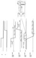
図1は、特許文献1に開示された従来のスイッチング回路の回路図である。このスイッチング回路は、駆動回路52と、主スイッチング素子51とで構成される。駆動回路52は、コンデンサ60、インバータ70、PMOSのトランジスタ53及びNMOSのトランジスタ54で構成される駆動信号発生回路と、駆動信号発生回路と主スイッチング素子51との間に接続された抵抗器55、56、58、59及びコンデンサ57とを備える。
図2は、特許文献2に開示された従来のスイッチング回路の回路図である。このスイッチング回路は、駆動信号発生回路80、スイッチング素子Q11、並びに、駆動信号発生回路80とスイッチング素子Q11との間に接続されたコンデンサC12及び逆バイアス電圧生成回路84で構成される。
そこで、上記特許文献1の技術における第1及び第2の問題、並びに、上記特許文献2の技術における第3及び第4の問題を解決するために、本発明に係るスイッチング回路は、ソース端子、ドレイン端子及びゲート端子を有するノーマリオフ型の接合型電界効果トランジスタと、第1の電源入力端子、前記第1の電源入力端子の電位又はハイインピーダンス状態を出力する第1の出力端子、第2の電源入力端子、前記第2の電源入力端子の電位又はハイインピーダンス状態を出力する第2の出力端子、及び、前記第1の出力端子が前記第1の電源入力端子の電位を出力し、かつ、前記第2の出力端子がハイインピーダンス状態を出力する第1の出力状態と、前記第1の出力端子がハイインピーダンス状態を出力し、かつ、前記第2の出力端子が前記第2の電源入力端子の電位を出力する第2の出力状態とを切り替えるための入力端子を有する駆動部と、前記ソース端子と前記ゲート端子との間に接続され、前記ソース端子側に陽極を有し、前記ゲート端子側に陰極を有する第1の整流素子と、前記第1の出力端子と前記ゲート端子との間に接続された第1の抵抗器と、前記第1の抵抗器と並列に接続された直列回路であって、直列に接続されたコンデンサと第2の抵抗器とを有する直列回路と、前記ゲート端子側に陽極を有し、前記第2の出力端子側に陰極を有する第2の整流素子とを備え、前記ソース端子は、前記第2の電源入力端子と接続され、前記第2の整流素子は、直列に接続された前記コンデンサ及び前記第2の抵抗器のうちの少なくとも前記コンデンサと並列に接続されている。
以下、本発明の実施の形態について、図面を用いて詳細に説明する。なお、以下で説明する実施の形態は、いずれも本発明の一具体例を示すものである。以下の実施の形態で示される数値、形状、材料、構成要素、構成要素の配置位置及び接続形態、波形、タイミング等は、一例であり、本発明を限定する主旨ではない。また、以下の実施の形態における構成要素のうち、本発明の最上位概念を示す独立請求項に記載されていない構成要素については、任意の構成要素として説明される。また、各図は、必ずしも厳密に図示したものではない。各図において、実質的に同一の構成については同一の符号を付し、重複する説明は省略又は簡略化する場合がある。
次に、上記実施の形態の変形例1に係るスイッチング回路40について説明する。
次に、上記実施の形態の変形例2に係るスイッチング回路41について説明する。
次に、上記実施の形態の変形例3に係るスイッチング回路42について説明する。
次に、上記実施の形態の変形例4に係るスイッチング回路43について説明する。
次に、上記実施の形態の変形例5に係るスイッチング回路44について説明する。
11、13 インバータ
12、14、16 電源
15 インダクタ
20、30、40~46 スイッチング回路
20a、30a 駆動部
21、22、31、32 スイッチ素子
23、24、33、34 抵抗器
25、35 コンデンサ
26、27、36、37、37b、37c、39 ダイオード
28、38 スイッチング素子
37a ツェナーダイオード
48 パッケージ
A、B 入力端子
V21、V31 第1の電源入力端子
V22、V32 第2の電源入力端子
IN21、IN31 入力端子
OUT21、OUT31 第1の出力端子
OUT22、OUT32 第2の出力端子
S21、S22、S23、S31、S32、S33 ソース端子
S31a 第1のソース端子
S31b 第2のソース端子
D21、D22、D23、D31、D32、D33 ドレイン端子
G21、G22、G23、G31、G32、G33 ゲート端子
Claims (11)
- ソース端子、ドレイン端子及びゲート端子を有するノーマリオフ型の接合型電界効果トランジスタと、
第1の電源入力端子、前記第1の電源入力端子の電位又はハイインピーダンス状態を出力する第1の出力端子、第2の電源入力端子、前記第2の電源入力端子の電位又はハイインピーダンス状態を出力する第2の出力端子、及び、前記第1の出力端子が前記第1の電源入力端子の電位を出力し、かつ、前記第2の出力端子がハイインピーダンス状態を出力する第1の出力状態と、前記第1の出力端子がハイインピーダンス状態を出力し、かつ、前記第2の出力端子が前記第2の電源入力端子の電位を出力する第2の出力状態とを切り替えるための入力端子を有する駆動部と、
前記ソース端子と前記ゲート端子との間に接続され、前記ソース端子側に陽極を有し、前記ゲート端子側に陰極を有する第1の整流素子と、
前記第1の出力端子と前記ゲート端子との間に接続された第1の抵抗器と、
前記第1の抵抗器と並列に接続された直列回路であって、直列に接続されたコンデンサと第2の抵抗器とを有する直列回路と、
前記ゲート端子側に陽極を有し、前記第2の出力端子側に陰極を有する第2の整流素子とを備え、
前記ソース端子は、前記第2の電源入力端子と接続され、
前記第2の整流素子は、直列に接続された前記コンデンサ及び前記第2の抵抗器のうちの少なくとも前記コンデンサと並列に接続されており、
前記コンデンサは、前記直列回路における前記ゲート端子側に接続され、前記第2の抵抗器は、前記直列回路における前記第1の出力端子側に接続されている
スイッチング回路。 - 前記第2の整流素子は、直列に接続された前記コンデンサ及び前記第2の抵抗器のうちの前記コンデンサだけと並列に接続されている
請求項1記載のスイッチング回路。 - 前記第2の整流素子は、直列に接続された前記コンデンサ及び前記第2の抵抗器と並列に接続されている
請求項1記載のスイッチング回路。 - さらに、前記第2の抵抗器と並列に接続され、前記コンデンサ側に陽極を有し、前記第1の抵抗器側に陰極を有する第3の整流素子を備える
請求項3記載のスイッチング回路。 - さらに、前記ソース端子と前記ゲート端子との間で、かつ、前記第1の整流素子と直列に接続され、前記ゲート端子側に陽極を有し、前記ソース端子側に陰極を有するツェナーダイオードを備える
請求項1~4のいずれか1項に記載のスイッチング回路。 - さらに、前記ソース端子と前記ゲート端子との間で、かつ、前記第1の整流素子と直列に接続され、前記ソース端子側に陽極を有し、前記ゲート端子側に陰極を有する少なくとも1つの整流素子を備える
請求項1~4のいずれか1項に記載のスイッチング回路。 - さらに、前記接合型電界効果トランジスタ、前記駆動部、前記第1の整流素子、前記第1の抵抗器、前記直列回路を構成する前記第2の抵抗器、及び、前記第2の整流素子を収容する単一のパッケージを備え、
前記パッケージは、前記コンデンサの両端のそれぞれと接続される第1の端子及び第2の端子、前記第1の整流素子の陽極と接続される第3の端子、並びに、前記ソース端子と接続される第4の端子を有し、
前記第1の端子は、前記第2の抵抗器と接続され、前記第2の端子は、前記ゲート端子と接続される
請求項1~4のいずれか1項に記載のスイッチング回路。 - さらに、前記パッケージの外部に配置され、前記第3の端子と前記第4の端子とを短絡する配線を備える
請求項7記載のスイッチング回路。 - さらに、前記パッケージの外部に配置され、前記第3の端子と前記第4の端子との間に接続され、前記第3の端子側に陽極を有し、前記第4の端子側に陰極を有するツェナーダイオードを備える
請求項7記載のスイッチング回路。 - さらに、前記パッケージの外部に配置され、前記第3の端子と前記第4の端子との間に接続され、前記第4の端子側に陽極を有し、前記第3の端子側に陰極を有する、直列に接続された複数の整流素子を備える
請求項7記載のスイッチング回路。 - 前記接合型電界効果トランジスタは、p型窒化物半導体、及び、前記p型窒化物半導体とオーミック接触するゲート電極で構成されるゲート部を有する
請求項1~10のいずれか1項に記載のスイッチング回路。
Priority Applications (1)
| Application Number | Priority Date | Filing Date | Title |
|---|---|---|---|
| JP2022189130A JP7457951B2 (ja) | 2018-02-28 | 2022-11-28 | スイッチング回路 |
Applications Claiming Priority (3)
| Application Number | Priority Date | Filing Date | Title |
|---|---|---|---|
| JP2018035949 | 2018-02-28 | ||
| JP2018035949 | 2018-02-28 | ||
| PCT/JP2019/000731 WO2019167446A1 (ja) | 2018-02-28 | 2019-01-11 | スイッチング回路 |
Related Child Applications (1)
| Application Number | Title | Priority Date | Filing Date |
|---|---|---|---|
| JP2022189130A Division JP7457951B2 (ja) | 2018-02-28 | 2022-11-28 | スイッチング回路 |
Publications (2)
| Publication Number | Publication Date |
|---|---|
| JPWO2019167446A1 JPWO2019167446A1 (ja) | 2021-02-25 |
| JP7369953B2 true JP7369953B2 (ja) | 2023-10-27 |
Family
ID=67808838
Family Applications (2)
| Application Number | Title | Priority Date | Filing Date |
|---|---|---|---|
| JP2020502843A Active JP7369953B2 (ja) | 2018-02-28 | 2019-01-11 | スイッチング回路 |
| JP2022189130A Active JP7457951B2 (ja) | 2018-02-28 | 2022-11-28 | スイッチング回路 |
Family Applications After (1)
| Application Number | Title | Priority Date | Filing Date |
|---|---|---|---|
| JP2022189130A Active JP7457951B2 (ja) | 2018-02-28 | 2022-11-28 | スイッチング回路 |
Country Status (5)
| Country | Link |
|---|---|
| US (2) | US11031935B2 (ja) |
| EP (2) | EP3761491B1 (ja) |
| JP (2) | JP7369953B2 (ja) |
| CN (2) | CN118868892A (ja) |
| WO (1) | WO2019167446A1 (ja) |
Families Citing this family (13)
| Publication number | Priority date | Publication date | Assignee | Title |
|---|---|---|---|---|
| EP3761491B1 (en) * | 2018-02-28 | 2025-08-06 | Panasonic Intellectual Property Management Co., Ltd. | Switching circuit |
| JP6981393B2 (ja) * | 2018-10-26 | 2021-12-15 | オムロン株式会社 | スイッチング素子の駆動回路及びスイッチング回路 |
| CN111835321A (zh) * | 2020-06-10 | 2020-10-27 | 深圳圣德京粤科技有限公司 | 一种脉冲宽度限制电路及方法 |
| CN113098240B (zh) * | 2021-03-31 | 2024-01-16 | 西北工业大学 | 一种Cascode型GaN功率器件的驱动电路 |
| US12212226B2 (en) * | 2021-06-28 | 2025-01-28 | Ancora Semiconductors Inc. | Conversion circuit |
| DE102021208085A1 (de) * | 2021-07-27 | 2023-02-02 | Robert Bosch Gesellschaft mit beschränkter Haftung | Vorrichtung und Verfahren zum Schalten einer Vielzahl von parallelgeschalteten Halbleitertransistoren |
| US11936383B2 (en) * | 2021-12-01 | 2024-03-19 | Tagore Technology, Inc. | Bias-less dynamic miller clamp |
| US20230216402A1 (en) * | 2022-01-04 | 2023-07-06 | Nuvolta Technologies (Hefei) Co., Ltd. | Gate Drive Voltage Regulation Apparatus and Control Method |
| TW202335204A (zh) * | 2022-02-25 | 2023-09-01 | 嘉和半導體股份有限公司 | 封裝結構 |
| EP4333305A1 (en) * | 2022-08-31 | 2024-03-06 | Nexperia B.V. | A voltage gate driver for a semiconductor-based transistor, as well as a power switch device, and a corresponding method |
| JP2024042823A (ja) * | 2022-09-16 | 2024-03-29 | ローム株式会社 | スイッチ装置、電子機器、車両 |
| US12334917B2 (en) * | 2022-12-16 | 2025-06-17 | United Silicon Carbide, Inc. | Voltage-source gate drive having shunt capacitors and shunt resistors |
| CN116318104A (zh) * | 2023-01-03 | 2023-06-23 | 台达电子企业管理(上海)有限公司 | 开关器件的驱动系统 |
Citations (1)
| Publication number | Priority date | Publication date | Assignee | Title |
|---|---|---|---|---|
| US20160261266A1 (en) | 2015-03-02 | 2016-09-08 | Infineon Technologies Austria Ag | Electronic Circuit |
Family Cites Families (23)
| Publication number | Priority date | Publication date | Assignee | Title |
|---|---|---|---|---|
| JP2605328B2 (ja) * | 1988-02-18 | 1997-04-30 | ソニー株式会社 | 共振形コンバータ |
| JPH0487373A (ja) * | 1990-07-31 | 1992-03-19 | Fujitsu Ltd | 半導体装置 |
| JPH04230116A (ja) * | 1990-12-27 | 1992-08-19 | Sanyo Electric Co Ltd | 電界効果トランジスタのドライブ回路 |
| DE19841733A1 (de) * | 1998-09-11 | 2000-03-16 | Siemens Ag | Stromversorgungseinrichtung |
| JP2002208850A (ja) * | 2000-11-13 | 2002-07-26 | Mitsubishi Electric Corp | 半導体スイッチ装置 |
| JP3978312B2 (ja) * | 2001-02-27 | 2007-09-19 | 三菱電機株式会社 | サイリスタ用ゲートドライバ |
| JP2007215389A (ja) | 2006-01-12 | 2007-08-23 | Hitachi Ltd | パワー半導体素子とこれを用いた半導体回路 |
| JP2013013044A (ja) * | 2011-05-31 | 2013-01-17 | Sanken Electric Co Ltd | ゲートドライブ回路 |
| CN104604134B (zh) * | 2012-08-30 | 2017-06-30 | 株式会社电装 | 半导体装置 |
| JP6163981B2 (ja) * | 2013-09-03 | 2017-07-19 | ダイキン工業株式会社 | 駆動装置および電力変換システム |
| JP2015208111A (ja) | 2014-04-21 | 2015-11-19 | ニチコン株式会社 | ゲート駆動回路 |
| JP2016040967A (ja) | 2014-08-12 | 2016-03-24 | ニチコン株式会社 | ゲート駆動回路 |
| JP2016096679A (ja) | 2014-11-14 | 2016-05-26 | パナソニックIpマネジメント株式会社 | ゲート駆動回路 |
| JP6419649B2 (ja) | 2015-05-28 | 2018-11-07 | ニチコン株式会社 | ゲート駆動回路 |
| WO2017081856A1 (ja) | 2015-11-09 | 2017-05-18 | パナソニックIpマネジメント株式会社 | スイッチング回路 |
| JP6477442B2 (ja) * | 2015-11-24 | 2019-03-06 | トヨタ自動車株式会社 | スイッチング回路及び電力変換回路 |
| US9998111B2 (en) * | 2015-12-16 | 2018-06-12 | Virginia Tech Intellectual Properties, Inc. | Power switch drivers with equalizers for paralleled switches |
| JP2018007539A (ja) | 2016-06-28 | 2018-01-11 | 富士電機株式会社 | 半導体装置 |
| US10826479B2 (en) * | 2016-07-06 | 2020-11-03 | Delta Electronics, Inc. | Waveform conversion circuit for gate driver |
| US10348286B2 (en) * | 2016-07-06 | 2019-07-09 | Delta Electronics, Inc. | Waveform conversion circuit for gate driver |
| US10826484B2 (en) * | 2016-07-06 | 2020-11-03 | Delta Electronics, Inc. | Waveform conversion circuit for gate driver |
| JP6645924B2 (ja) * | 2016-07-12 | 2020-02-14 | 株式会社東芝 | 半導体装置及び電力変換装置 |
| EP3761491B1 (en) * | 2018-02-28 | 2025-08-06 | Panasonic Intellectual Property Management Co., Ltd. | Switching circuit |
-
2019
- 2019-01-11 EP EP19761119.7A patent/EP3761491B1/en active Active
- 2019-01-11 WO PCT/JP2019/000731 patent/WO2019167446A1/ja not_active Ceased
- 2019-01-11 CN CN202410877692.1A patent/CN118868892A/zh active Pending
- 2019-01-11 CN CN201980014358.0A patent/CN111771322B/zh active Active
- 2019-01-11 EP EP21199382.9A patent/EP3955442B1/en active Active
- 2019-01-11 JP JP2020502843A patent/JP7369953B2/ja active Active
-
2020
- 2020-08-26 US US17/003,900 patent/US11031935B2/en active Active
-
2021
- 2021-05-05 US US17/308,805 patent/US11398820B2/en active Active
-
2022
- 2022-11-28 JP JP2022189130A patent/JP7457951B2/ja active Active
Patent Citations (1)
| Publication number | Priority date | Publication date | Assignee | Title |
|---|---|---|---|---|
| US20160261266A1 (en) | 2015-03-02 | 2016-09-08 | Infineon Technologies Austria Ag | Electronic Circuit |
Also Published As
| Publication number | Publication date |
|---|---|
| EP3955442B1 (en) | 2025-03-05 |
| CN111771322B (zh) | 2024-09-17 |
| US20210258008A1 (en) | 2021-08-19 |
| JP2023016898A (ja) | 2023-02-02 |
| CN111771322A (zh) | 2020-10-13 |
| WO2019167446A1 (ja) | 2019-09-06 |
| EP3761491B1 (en) | 2025-08-06 |
| CN118868892A (zh) | 2024-10-29 |
| EP3761491A4 (en) | 2021-04-21 |
| JPWO2019167446A1 (ja) | 2021-02-25 |
| US20200395933A1 (en) | 2020-12-17 |
| EP3955442A1 (en) | 2022-02-16 |
| JP7457951B2 (ja) | 2024-03-29 |
| EP3761491A1 (en) | 2021-01-06 |
| US11398820B2 (en) | 2022-07-26 |
| US11031935B2 (en) | 2021-06-08 |
Similar Documents
| Publication | Publication Date | Title |
|---|---|---|
| JP7457951B2 (ja) | スイッチング回路 | |
| CN111193395B (zh) | 基于零电流检测的谐振转换器控制 | |
| CN111799992B (zh) | GaN半桥电路和GaN自举电源电压发生器电路 | |
| US10305472B1 (en) | Half bridge driver circuits | |
| US9741702B2 (en) | Semiconductor power modules and devices | |
| US10404256B2 (en) | Capacitively coupled level shifter | |
| US8766711B2 (en) | Switching circuit with controlled driver circuit | |
| CN114172123B (zh) | 半导体装置 | |
| JP5991939B2 (ja) | 半導体デバイス駆動回路および半導体デバイス駆動装置 | |
| WO2017081856A1 (ja) | スイッチング回路 | |
| US8638134B2 (en) | Gate drive circuit and power semiconductor module | |
| US9871513B2 (en) | Semiconductor device | |
| KR101329610B1 (ko) | 반도체장치 | |
| US20240204774A1 (en) | Voltage-source gate drive having shunt capacitors and shunt resistors | |
| JP6950443B2 (ja) | 半導体スイッチング素子駆動回路及び電力変換器 | |
| CN119631289A (zh) | 半导体装置以及电力变换装置 | |
| CN111416602A (zh) | 半导体装置 | |
| JP7634237B2 (ja) | 開閉装置用回路、開閉システム、及び開閉装置用処理方法 | |
| CN118214256A (zh) | 具有分流电容器和分流电阻器的电压源栅极驱动器 |
Legal Events
| Date | Code | Title | Description |
|---|---|---|---|
| A621 | Written request for application examination |
Free format text: JAPANESE INTERMEDIATE CODE: A621 Effective date: 20211124 |
|
| A131 | Notification of reasons for refusal |
Free format text: JAPANESE INTERMEDIATE CODE: A131 Effective date: 20220830 |
|
| A601 | Written request for extension of time |
Free format text: JAPANESE INTERMEDIATE CODE: A601 Effective date: 20221025 |
|
| A521 | Request for written amendment filed |
Free format text: JAPANESE INTERMEDIATE CODE: A523 Effective date: 20221128 |
|
| A131 | Notification of reasons for refusal |
Free format text: JAPANESE INTERMEDIATE CODE: A131 Effective date: 20230328 |
|
| A521 | Request for written amendment filed |
Free format text: JAPANESE INTERMEDIATE CODE: A523 Effective date: 20230529 |
|
| TRDD | Decision of grant or rejection written | ||
| A01 | Written decision to grant a patent or to grant a registration (utility model) |
Free format text: JAPANESE INTERMEDIATE CODE: A01 Effective date: 20230912 |
|
| A61 | First payment of annual fees (during grant procedure) |
Free format text: JAPANESE INTERMEDIATE CODE: A61 Effective date: 20231004 |
|
| R151 | Written notification of patent or utility model registration |
Ref document number: 7369953 Country of ref document: JP Free format text: JAPANESE INTERMEDIATE CODE: R151 |