JP7401823B2 - 光導波路部品およびその製造方法 - Google Patents
光導波路部品およびその製造方法 Download PDFInfo
- Publication number
- JP7401823B2 JP7401823B2 JP2022544918A JP2022544918A JP7401823B2 JP 7401823 B2 JP7401823 B2 JP 7401823B2 JP 2022544918 A JP2022544918 A JP 2022544918A JP 2022544918 A JP2022544918 A JP 2022544918A JP 7401823 B2 JP7401823 B2 JP 7401823B2
- Authority
- JP
- Japan
- Prior art keywords
- core
- optical waveguide
- optical
- sio
- cladding
- Prior art date
- Legal status (The legal status is an assumption and is not a legal conclusion. Google has not performed a legal analysis and makes no representation as to the accuracy of the status listed.)
- Active
Links
Images



Classifications
-
- G—PHYSICS
- G02—OPTICS
- G02B—OPTICAL ELEMENTS, SYSTEMS OR APPARATUS
- G02B6/00—Light guides; Structural details of arrangements comprising light guides and other optical elements, e.g. couplings
- G02B6/02—Optical fibres with cladding with or without a coating
- G02B6/02004—Optical fibres with cladding with or without a coating characterised by the core effective area or mode field radius
-
- G—PHYSICS
- G02—OPTICS
- G02B—OPTICAL ELEMENTS, SYSTEMS OR APPARATUS
- G02B6/00—Light guides; Structural details of arrangements comprising light guides and other optical elements, e.g. couplings
- G02B6/10—Light guides; Structural details of arrangements comprising light guides and other optical elements, e.g. couplings of the optical waveguide type
- G02B6/12—Light guides; Structural details of arrangements comprising light guides and other optical elements, e.g. couplings of the optical waveguide type of the integrated circuit kind
- G02B6/122—Basic optical elements, e.g. light-guiding paths
- G02B6/1228—Tapered waveguides, e.g. integrated spot-size transformers
-
- G—PHYSICS
- G02—OPTICS
- G02B—OPTICAL ELEMENTS, SYSTEMS OR APPARATUS
- G02B6/00—Light guides; Structural details of arrangements comprising light guides and other optical elements, e.g. couplings
- G02B6/10—Light guides; Structural details of arrangements comprising light guides and other optical elements, e.g. couplings of the optical waveguide type
- G02B6/12—Light guides; Structural details of arrangements comprising light guides and other optical elements, e.g. couplings of the optical waveguide type of the integrated circuit kind
- G02B6/12007—Light guides; Structural details of arrangements comprising light guides and other optical elements, e.g. couplings of the optical waveguide type of the integrated circuit kind forming wavelength selective elements, e.g. multiplexer, demultiplexer
- G02B6/12009—Light guides; Structural details of arrangements comprising light guides and other optical elements, e.g. couplings of the optical waveguide type of the integrated circuit kind forming wavelength selective elements, e.g. multiplexer, demultiplexer comprising arrayed waveguide grating [AWG] devices, i.e. with a phased array of waveguides
- G02B6/12016—Light guides; Structural details of arrangements comprising light guides and other optical elements, e.g. couplings of the optical waveguide type of the integrated circuit kind forming wavelength selective elements, e.g. multiplexer, demultiplexer comprising arrayed waveguide grating [AWG] devices, i.e. with a phased array of waveguides characterised by the input or output waveguides, e.g. tapered waveguide ends, coupled together pairs of output waveguides
-
- G—PHYSICS
- G02—OPTICS
- G02B—OPTICAL ELEMENTS, SYSTEMS OR APPARATUS
- G02B6/00—Light guides; Structural details of arrangements comprising light guides and other optical elements, e.g. couplings
- G02B6/10—Light guides; Structural details of arrangements comprising light guides and other optical elements, e.g. couplings of the optical waveguide type
- G02B6/12—Light guides; Structural details of arrangements comprising light guides and other optical elements, e.g. couplings of the optical waveguide type of the integrated circuit kind
- G02B2006/12035—Materials
-
- G—PHYSICS
- G02—OPTICS
- G02B—OPTICAL ELEMENTS, SYSTEMS OR APPARATUS
- G02B6/00—Light guides; Structural details of arrangements comprising light guides and other optical elements, e.g. couplings
- G02B6/10—Light guides; Structural details of arrangements comprising light guides and other optical elements, e.g. couplings of the optical waveguide type
- G02B6/12—Light guides; Structural details of arrangements comprising light guides and other optical elements, e.g. couplings of the optical waveguide type of the integrated circuit kind
- G02B2006/12083—Constructional arrangements
- G02B2006/12088—Monomode
-
- G—PHYSICS
- G02—OPTICS
- G02B—OPTICAL ELEMENTS, SYSTEMS OR APPARATUS
- G02B6/00—Light guides; Structural details of arrangements comprising light guides and other optical elements, e.g. couplings
- G02B6/24—Coupling light guides
- G02B6/26—Optical coupling means
- G02B6/30—Optical coupling means for use between fibre and thin-film device
- G02B6/305—Optical coupling means for use between fibre and thin-film device and having an integrated mode-size expanding section, e.g. tapered waveguide
Landscapes
- Physics & Mathematics (AREA)
- General Physics & Mathematics (AREA)
- Optics & Photonics (AREA)
- Engineering & Computer Science (AREA)
- Microelectronics & Electronic Packaging (AREA)
- Power Engineering (AREA)
- Optical Integrated Circuits (AREA)
Description
このピッチ変換配線パターンでは、元々高密度に配置された数μmのコア間ピッチをSMF接続のために100μm以上にまで拡大させる必要があり、シリコン光回路が大型化したり、配線長が長くなったりしてしまう。シリコンフォトニクスは光回路の高密度集積化には優れているが、シリコン細線導波路の伝搬損失は3dB/cmに及ぶ。シリコン光回路内の極小領域では問題とならなかった伝搬損失が、今度は、光回路全体が大型化し配線長が長距離化することで、深刻な問題となっていた。このようなシリコン光回路とSMFの間の接続性に関する問題を解決するために、スポットサイズ変換構造(Spot Size Conversion:SSC)およびピッチ変換構造を挿入する手法が提案されていた。
本発明はこのような問題に鑑みなされたものであり、異なる材料の異なる光導波路を低損失で低コストに提供できる新規な光導波路構造およびその製造方法を提供する。
n1 > n2 > n3 式(1)
[第1の実施形態:光導波路の構成]
図1の光導波路部品100には、2種類の光導波路が存在している。すなわち1つは、SiO2コア部103-1aをアンダークラッド、Siコア104をコア、SiO2コア部103-1bをオーバークラッドとする第1の光導波路110である。もう1つは、SiO2層102をアンダークラッド、SiO2コア103をコア、SiO2層105をオーバークラッドとする第2の光導波路120である。
[各層の厚み、中心高さ合わせ構造]
ここで再び図1の光導波路部品100に戻ると、アンダークラッドのSiO2層102およびオーバークラッドのSiO2層105の厚さは、第2の光導波路120のSiO2コア103内を伝搬する光のモードフィールドが十分収まるものであれば良い。すなわちクラッド層102、105は、第2の光導波路120を伝搬する光のモードフィールドが、基板101やオーバークラッドSiO2層105直上の空気層にまで染み出さない程度の厚さであれば良い。一般的には、クラッドSiO2層102、105の厚さは数10μm程度であれば十分である。
[モード数の非限定、コアサイズ、シングルモードの場合のMFD]
図1の光導波路部品100において、第1の光導波路110および第2の光導波路120のいずれも、コア断面サイズに上限はなく、使用する光信号の波長に対して、複数のモードの光を伝搬させるマルチモードの光導波路とすることもできる。また、コア断面サイズを小さくすることで、最低次のモードのみを伝搬させるシングルモードの光導波路とすることもできる。
[結合方式]
シングルモードとなる光導波路のコア同士を接続させる方式は、2種類に大別される。1つの接続方式は断熱結合であり、伝搬方向に対して、2つの光導波路の両コアが接するように配置し、一方の光導波路コアを、先細りのテーパ形状にするなどしてコア内を伝搬するモードの等価屈折率を徐々に減少させる。このような構成により、もはや閉じ込めきれなくなったモードの光エネルギーが、隣接する他方の光導波路コアへと断熱的に遷移する。もう1つの接続方式は突合せ結合であり、コアどうしの端面を突き合わせて配置し、2つの光導波路の両コアに存在するモードプロファイルの重なり積分でその結合効率が規定される。
[第2の実施形態:ピッチ変換]
図3は、第2の実施形態の光導波路部品の構成を示す図である。第2の実施形態の光導波路部品300では、複数の第1の光導波路と、同数の第2の光導波路とを低損失に結合する。複数の第1の光導波路の内の1つの第1の光導波路と、対応する第2の光導波路との間の構造は、図1に示した第1の実施形態の光導波路部品100と同様であり、説明を省略する。
[第3の実施形態:製造方法]
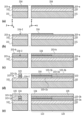
図4は、本開示の光導波路部品の製造方法のプロセスを説明する図である。本実施形態は、第1の実施形態および第2の実施形態で示した光導波路部品の製造方法であり、作製される光導波路部品の構造については、第1の実施形態および第2の実施形態に記載の通りであるため、説明を省略する。図4の(a)~(e)は、図1の光導波路部品100が作製されるまでステップを順に示している。
Claims (5)
- 基板の上に、
複数の第1の光導波路と、
前記第1の光導波路とは異なるモードフィールド径(MFD)を持ち、前記第1の光導波路と光学的に結合した、対応する複数の第2の光導波路とを有する光導波路部品であって、
前記複数の第2の光導波路は、前記複数の第1の光導波路とは異なる間隔で配置されており、前記複数の第1の光導波路と前記複数の第2の光導波路の間に、導波路間間隔を拡張する領域を有し、
前記複数の第1の光導波路の各々は、
第1の材料による第1のコア、および、前記第1のコアの上下に形成された、第2の材料によるクラッドを含み、
前記複数の第2の光導波路の各々は、
前記第1のコアに沿って、前記クラッドから延長して形成された前記第2の材料による第2のコア、前記基板と前記第2のコアの間に形成された、第3の材料による下側クラッド、および、前記第2のコアの上に形成された上側クラッドを含み、
前記光導波路の長さ方向に垂直な断面において、前記第1のコアの領域は、前記第2のコアの領域に内包されており、
前記第1の材料は最も屈折率が大きく、前記第3の材料は最も屈折率が小さく、
前記第1のコアの先端部は、前記第1のコアが断続的に形成されたセグメント構造を有し、前記第1の光導波路を伝搬する光信号のMFDを変化させるスポットサイズ変換領域を構成しており、
前記第1の光導波路の前記第1のコアから延長して形成された第3のコア、および、前記第1の光導波路の前記第1のコアの下に形成された前記クラッドから延長して形成された下側クラッドのみを含む、前記スポットサイズ変換領域の外に形成された第3の光導波路をさらに備えた
ことを特徴とする光導波路部品。 - 前記第3の光導波路は、
前記第3のコアの上が、前記第2の光導波路の前記上側クラッドから延長して形成された上側クラッドでさらに覆われていることを特徴とする請求項1に記載の光導波路部品。 - 前記第1のコアの下に形成された前記クラッドの厚さは、前記第2のコアの高さの1/2および前記第1のコアの高さの1/2の間の差に設定されており、
前記第1のコアの中心高さおよび前記第2のコアの中心高さが一致することを特徴とする請求項1または2に記載の光導波路部品。 - 前記第1の光導波路および前記第2の光導波路は、導波する光信号波長に対してシングルモード導波路であることを特徴とする請求項1乃至3いずれかに記載の光導波路部品。
- 前記第1の材料、前記第2の材料および前記第3の材料は、Si、SiN、SiON、SiOX、ポリマーのいずれかを母材とし、
前記母材の違いによって屈折率の違いが生じたもの、または、
前記母材への不純物の添加量の違いによって屈折率の違いが生じたもののいずれかであること特徴とする請求項1乃至4いずれかに記載の光導波路部品。
Applications Claiming Priority (1)
| Application Number | Priority Date | Filing Date | Title |
|---|---|---|---|
| PCT/JP2020/031934 WO2022044101A1 (ja) | 2020-08-25 | 2020-08-25 | 光導波路部品およびその製造方法 |
Publications (2)
| Publication Number | Publication Date |
|---|---|
| JPWO2022044101A1 JPWO2022044101A1 (ja) | 2022-03-03 |
| JP7401823B2 true JP7401823B2 (ja) | 2023-12-20 |
Family
ID=80352802
Family Applications (1)
| Application Number | Title | Priority Date | Filing Date |
|---|---|---|---|
| JP2022544918A Active JP7401823B2 (ja) | 2020-08-25 | 2020-08-25 | 光導波路部品およびその製造方法 |
Country Status (3)
| Country | Link |
|---|---|
| US (1) | US20230280524A1 (ja) |
| JP (1) | JP7401823B2 (ja) |
| WO (1) | WO2022044101A1 (ja) |
Families Citing this family (1)
| Publication number | Priority date | Publication date | Assignee | Title |
|---|---|---|---|---|
| CN121175605A (zh) * | 2023-05-24 | 2025-12-19 | 三菱电机株式会社 | 光斑尺寸转换器 |
Citations (6)
| Publication number | Priority date | Publication date | Assignee | Title |
|---|---|---|---|---|
| JP2004258610A (ja) | 2003-02-04 | 2004-09-16 | Tdk Corp | スポットサイズ変換素子及びその製造方法並びにスポットサイズ変換素子を用いた導波路埋め込み型光回路 |
| JP2005538426A (ja) | 2002-08-20 | 2005-12-15 | エルエヌエル・テクノロジーズ・インコーポレイテッド | 埋め込みモードコンバータ |
| US20090297093A1 (en) | 2008-05-28 | 2009-12-03 | Lightwire, Inc. | Low index, large mode field diameter optical coupler |
| WO2012114866A1 (ja) | 2011-02-21 | 2012-08-30 | 日本電気株式会社 | スポットサイズ変換器及びその製造方法 |
| JP2016018191A (ja) | 2014-07-11 | 2016-02-01 | 沖電気工業株式会社 | スポットサイズ変換器及びその製造方法 |
| US20190310423A1 (en) | 2018-04-04 | 2019-10-10 | Finisar Corporation | Adiabatically coupled photonic systems with fan-out interposer |
Family Cites Families (1)
| Publication number | Priority date | Publication date | Assignee | Title |
|---|---|---|---|---|
| JPH05249331A (ja) * | 1992-01-09 | 1993-09-28 | Nippon Telegr & Teleph Corp <Ntt> | 導波路形ビームスポット変換素子およびその製造方法 |
-
2020
- 2020-08-25 WO PCT/JP2020/031934 patent/WO2022044101A1/ja not_active Ceased
- 2020-08-25 JP JP2022544918A patent/JP7401823B2/ja active Active
- 2020-08-25 US US18/005,711 patent/US20230280524A1/en not_active Abandoned
Patent Citations (6)
| Publication number | Priority date | Publication date | Assignee | Title |
|---|---|---|---|---|
| JP2005538426A (ja) | 2002-08-20 | 2005-12-15 | エルエヌエル・テクノロジーズ・インコーポレイテッド | 埋め込みモードコンバータ |
| JP2004258610A (ja) | 2003-02-04 | 2004-09-16 | Tdk Corp | スポットサイズ変換素子及びその製造方法並びにスポットサイズ変換素子を用いた導波路埋め込み型光回路 |
| US20090297093A1 (en) | 2008-05-28 | 2009-12-03 | Lightwire, Inc. | Low index, large mode field diameter optical coupler |
| WO2012114866A1 (ja) | 2011-02-21 | 2012-08-30 | 日本電気株式会社 | スポットサイズ変換器及びその製造方法 |
| JP2016018191A (ja) | 2014-07-11 | 2016-02-01 | 沖電気工業株式会社 | スポットサイズ変換器及びその製造方法 |
| US20190310423A1 (en) | 2018-04-04 | 2019-10-10 | Finisar Corporation | Adiabatically coupled photonic systems with fan-out interposer |
Also Published As
| Publication number | Publication date |
|---|---|
| JPWO2022044101A1 (ja) | 2022-03-03 |
| US20230280524A1 (en) | 2023-09-07 |
| WO2022044101A1 (ja) | 2022-03-03 |
Similar Documents
| Publication | Publication Date | Title |
|---|---|---|
| US9128240B2 (en) | Spot-size converter, manufacturing method thereof, and integrated optical circuit device | |
| US8000565B2 (en) | Buried dual taper waveguide for passive alignment and photonic integration | |
| US20190265415A1 (en) | Optical apparatus and methods of manufacture thereof | |
| KR101121459B1 (ko) | 광섬유 및 평면 광학 도파관을 치밀하게 결합하는 방법 및장치 | |
| WO2018113627A1 (en) | Optical edge coupler with controllable mode field for photonic chip | |
| JP6290742B2 (ja) | 光回路部品、および光回路部品と光ファイバとの接続構造 | |
| US20060115215A1 (en) | Dual "cheese wedge" silicon taper waveguide | |
| CA2734614A1 (en) | Optical mode transformer, in particular for coupling an optical fiber and a high-index contrast waveguide | |
| CN112269224B (zh) | 基于垂直耦合结构的硅-氮化硅集成偏振分束器 | |
| US20240393532A1 (en) | Relaxed tolerance adiabatic coupler for optical interconnects | |
| CN112305671B (zh) | 基于狭缝波导的锥形偏振分束器及制备方法 | |
| JP2002122750A (ja) | 光導波路接続構造 | |
| CN116804784A (zh) | 具有连续布置的锥的边缘耦合器 | |
| CN115079341B (zh) | 一种波导器件 | |
| CN210666088U (zh) | 一种硅光光模斑模式转换器 | |
| WO2021178727A1 (en) | Evanescent coupler mode converters | |
| JP7401823B2 (ja) | 光導波路部品およびその製造方法 | |
| JP7725960B2 (ja) | 光集積素子、光集積回路ウエハ及び光集積素子の製造方法 | |
| JP5438080B2 (ja) | スポットサイズ変換器 | |
| JP2004157530A (ja) | 光モジュール | |
| CN112470047A (zh) | 用于混合器件的二氧化硅到氮化硅plc波型变换器 | |
| JP7828019B2 (ja) | 光導波回路および光導波回路の製造方法 | |
| JP7401824B2 (ja) | 光導波路部品およびその製造方法 | |
| JP7568986B2 (ja) | 光導波回路およびその製造方法 | |
| JP7776787B2 (ja) | 光導波路接続構造 |
Legal Events
| Date | Code | Title | Description |
|---|---|---|---|
| A621 | Written request for application examination |
Free format text: JAPANESE INTERMEDIATE CODE: A621 Effective date: 20221125 |
|
| A131 | Notification of reasons for refusal |
Free format text: JAPANESE INTERMEDIATE CODE: A131 Effective date: 20230704 |
|
| A521 | Request for written amendment filed |
Free format text: JAPANESE INTERMEDIATE CODE: A523 Effective date: 20230815 |
|
| TRDD | Decision of grant or rejection written | ||
| A01 | Written decision to grant a patent or to grant a registration (utility model) |
Free format text: JAPANESE INTERMEDIATE CODE: A01 Effective date: 20231107 |
|
| A61 | First payment of annual fees (during grant procedure) |
Free format text: JAPANESE INTERMEDIATE CODE: A61 Effective date: 20231120 |
|
| R150 | Certificate of patent or registration of utility model |
Ref document number: 7401823 Country of ref document: JP Free format text: JAPANESE INTERMEDIATE CODE: R150 |
|
| S533 | Written request for registration of change of name |
Free format text: JAPANESE INTERMEDIATE CODE: R313533 |
|
| R350 | Written notification of registration of transfer |
Free format text: JAPANESE INTERMEDIATE CODE: R350 |