JP7420060B2 - Single crystal manufacturing equipment - Google Patents
Single crystal manufacturing equipment Download PDFInfo
- Publication number
- JP7420060B2 JP7420060B2 JP2020205263A JP2020205263A JP7420060B2 JP 7420060 B2 JP7420060 B2 JP 7420060B2 JP 2020205263 A JP2020205263 A JP 2020205263A JP 2020205263 A JP2020205263 A JP 2020205263A JP 7420060 B2 JP7420060 B2 JP 7420060B2
- Authority
- JP
- Japan
- Prior art keywords
- single crystal
- tube
- cooling
- cylinder
- auxiliary
- Prior art date
- Legal status (The legal status is an assumption and is not a legal conclusion. Google has not performed a legal analysis and makes no representation as to the accuracy of the status listed.)
- Active
Links
- 239000013078 crystal Substances 0.000 title claims description 157
- 238000004519 manufacturing process Methods 0.000 title claims description 72
- 238000001816 cooling Methods 0.000 claims description 131
- XUIMIQQOPSSXEZ-UHFFFAOYSA-N Silicon Chemical compound [Si] XUIMIQQOPSSXEZ-UHFFFAOYSA-N 0.000 claims description 111
- 229910052710 silicon Inorganic materials 0.000 claims description 111
- 239000010703 silicon Substances 0.000 claims description 111
- OKTJSMMVPCPJKN-UHFFFAOYSA-N Carbon Chemical compound [C] OKTJSMMVPCPJKN-UHFFFAOYSA-N 0.000 claims description 100
- 229910052799 carbon Inorganic materials 0.000 claims description 86
- 239000010453 quartz Substances 0.000 claims description 22
- VYPSYNLAJGMNEJ-UHFFFAOYSA-N silicon dioxide Inorganic materials O=[Si]=O VYPSYNLAJGMNEJ-UHFFFAOYSA-N 0.000 claims description 22
- 238000000034 method Methods 0.000 claims description 20
- 229910002804 graphite Inorganic materials 0.000 claims description 16
- 239000010439 graphite Substances 0.000 claims description 16
- 239000002826 coolant Substances 0.000 claims description 8
- ZOKXTWBITQBERF-UHFFFAOYSA-N Molybdenum Chemical compound [Mo] ZOKXTWBITQBERF-UHFFFAOYSA-N 0.000 claims description 3
- 239000002131 composite material Substances 0.000 claims description 3
- 229910052750 molybdenum Inorganic materials 0.000 claims description 3
- 239000011733 molybdenum Substances 0.000 claims description 3
- 229910001220 stainless steel Inorganic materials 0.000 claims description 3
- 239000010935 stainless steel Substances 0.000 claims description 3
- WFKWXMTUELFFGS-UHFFFAOYSA-N tungsten Chemical compound [W] WFKWXMTUELFFGS-UHFFFAOYSA-N 0.000 claims description 3
- 229910052721 tungsten Inorganic materials 0.000 claims description 3
- 239000010937 tungsten Substances 0.000 claims description 3
- 230000000052 comparative effect Effects 0.000 description 31
- 239000007789 gas Substances 0.000 description 27
- 239000002994 raw material Substances 0.000 description 17
- 238000006243 chemical reaction Methods 0.000 description 15
- 230000000694 effects Effects 0.000 description 12
- 238000005516 engineering process Methods 0.000 description 7
- 238000007711 solidification Methods 0.000 description 7
- 230000008023 solidification Effects 0.000 description 7
- 239000011261 inert gas Substances 0.000 description 6
- 239000000463 material Substances 0.000 description 5
- 235000012431 wafers Nutrition 0.000 description 5
- 238000011109 contamination Methods 0.000 description 4
- 239000000155 melt Substances 0.000 description 4
- 238000012544 monitoring process Methods 0.000 description 3
- 239000004065 semiconductor Substances 0.000 description 3
- 150000001721 carbon Chemical class 0.000 description 2
- 230000007423 decrease Effects 0.000 description 2
- 239000012535 impurity Substances 0.000 description 2
- 239000011810 insulating material Substances 0.000 description 2
- 229910052751 metal Inorganic materials 0.000 description 2
- 239000002184 metal Substances 0.000 description 2
- 239000005416 organic matter Substances 0.000 description 2
- 238000003892 spreading Methods 0.000 description 2
- 230000007480 spreading Effects 0.000 description 2
- 239000000758 substrate Substances 0.000 description 2
- 239000004698 Polyethylene Substances 0.000 description 1
- 239000000919 ceramic Substances 0.000 description 1
- 238000004891 communication Methods 0.000 description 1
- 238000007796 conventional method Methods 0.000 description 1
- 239000002019 doping agent Substances 0.000 description 1
- 239000007770 graphite material Substances 0.000 description 1
- 229910001385 heavy metal Inorganic materials 0.000 description 1
- 229930195733 hydrocarbon Natural products 0.000 description 1
- 150000002430 hydrocarbons Chemical class 0.000 description 1
- 230000008676 import Effects 0.000 description 1
- 238000009413 insulation Methods 0.000 description 1
- 239000012212 insulator Substances 0.000 description 1
- 238000005259 measurement Methods 0.000 description 1
- 230000007246 mechanism Effects 0.000 description 1
- 238000002844 melting Methods 0.000 description 1
- 230000008018 melting Effects 0.000 description 1
- 239000000178 monomer Substances 0.000 description 1
- -1 polyethylene Polymers 0.000 description 1
- 229920000573 polyethylene Polymers 0.000 description 1
- 230000008569 process Effects 0.000 description 1
- 230000005855 radiation Effects 0.000 description 1
- 230000009467 reduction Effects 0.000 description 1
- 238000003860 storage Methods 0.000 description 1
- 238000012546 transfer Methods 0.000 description 1
Images


Landscapes
- Crystals, And After-Treatments Of Crystals (AREA)
Description
本発明は、単結晶製造装置に関する。 The present invention relates to a single crystal manufacturing apparatus.
携帯電話など通信用にRF(高周波)デバイスが用いられている。 RF (radio frequency) devices are used for communication such as mobile phones.
シリコン単結晶ウェーハを用いたRFデバイスにおいては、基板抵抗率が低いと高導電性のために損失が大きいため、1000Ωcm以上の高抵抗率、すなわち抵抗率に関わるBやPなどのドーパント濃度が非常に低いウェーハが用いられる。 In RF devices using silicon single crystal wafers, if the substrate resistivity is low, the loss is large due to high conductivity. A low wafer is used.
SOI(Silicon on Insulator)と呼ばれる、シリコン基板表層部に薄い酸化膜+薄いシリコン層が形成されたウェーハを用いることもあるが、この場合も高抵抗率が望まれる。 A wafer called SOI (Silicon on Insulator) in which a thin oxide film and a thin silicon layer are formed on the surface of a silicon substrate is sometimes used, but high resistivity is also desired in this case.
またパワーデバイス用としても、高耐圧用として比較的高抵抗率ウェーハが望まれている上、IGBTなどでは良好な特性を得るために、炭素濃度が極めて低いシリコン単結晶ウェーハが要求されるようになってきている。つまり最新の半導体デバイスにおいては、重金属などの不純物はもとより、ドーパントや軽元素である炭素など、不純物の低減は必須の課題となっている。 Also, for power devices, relatively high resistivity wafers are desired for high voltage applications, and silicon single crystal wafers with extremely low carbon concentration are required for IGBTs and other devices to obtain good characteristics. It has become to. In other words, in the latest semiconductor devices, it is essential to reduce impurities such as heavy metals and other impurities, as well as dopants and the light element carbon.
シリコン単結晶中に混入する炭素は、原料からの持ち込みに起因するものと、結晶製造プロセス中の炉内反応に起因したものとの2つが挙げられ、これらの各導入過程別に炭素濃度低減を試みた技術が報告されている。 There are two types of carbon mixed into silicon single crystals: one is brought in from raw materials, and the other is caused by reactions in the furnace during the crystal manufacturing process. We are trying to reduce the carbon concentration in each of these introduction processes. A new technology has been reported.
原料からの持ち込みについては、原料シリコンの表面に付着した有機物の中には高温で気化せず炭化するものがあり、これが結晶中に取り込まれることで結晶中の炭素濃度が上昇するという問題がある。 Regarding the import from raw materials, there is a problem that some organic matter attached to the surface of raw silicon does not vaporize at high temperatures but carbonizes, and when this is incorporated into the crystal, the carbon concentration in the crystal increases. .
これを改善するために、例えば、特許文献1のパラフィン系炭化水素をはじめとする有機物汚染が少ないポリエチレン製収容袋に保管した多結晶原料を用いてCZ法で単結晶育成を行う方法、特許文献2の多結晶表面の有機物を同定して定量分析し、原料選別した後に、CZ法で単結晶育成を行う方法が挙げられる。
In order to improve this, for example, a method of growing single crystals by the CZ method using a polycrystalline raw material stored in a polyethylene storage bag with little organic contamination including paraffinic hydrocarbons as described in Patent Document 1, Patent Document 1 An example of
他方、結晶製造プロセスに起因した炭素の混入については、結晶育成中に引上げ機炉内の炭素部材とシリコン融液から蒸発するSiOの反応によって炉内に炭素含有ガスが生成され、この炭素含有ガスが融液中に混入することで炭素濃度が上昇するという問題がある。 On the other hand, regarding the contamination of carbon due to the crystal manufacturing process, carbon-containing gas is generated in the furnace due to the reaction between carbon members in the puller furnace and SiO evaporated from the silicon melt during crystal growth, and this carbon-containing gas There is a problem in that carbon concentration increases due to mixing of carbon into the melt.
この問題を解決するために、例えば、特許文献3の黒鉛ルツボの上に円筒形状の整流部材を搭載し、炭素含有ガスの融液側への逆流を防ぐ方法がある。また、整流部材を搭載して単結晶育成を行う他の例として、特許文献4のルツボの上方に石英製の整流筒とカーボン製の整流筒を搭載する方法や、特許文献5のルツボの上方に石英製の整流筒のみを搭載する方法がある。
To solve this problem, for example, there is a method disclosed in Patent Document 3, in which a cylindrical rectifying member is mounted on the graphite crucible to prevent the carbon-containing gas from flowing back toward the melt side. Other examples of growing single crystals by mounting a rectifying member include a method of mounting a quartz rectifying tube and a carbon rectifying tube above a crucible in
上記の整流部材を用いて単結晶育成を行うことで、シリコン原料融液直上から石英ルツボ上端の方向に流れる不活性ガスの線速を上昇させることができ、これにより炉内の炭素部材とシリコン融液から蒸発するSiOの反応によって生じた炭素含有ガスが原料融液側に逆流することを防ぐことができ、その結果として、整流部材なしの場合に比べて低い炭素濃度の単結晶を育成することが可能となる。 By growing a single crystal using the above-mentioned rectifying member, it is possible to increase the linear velocity of the inert gas flowing from directly above the silicon raw material melt toward the top of the quartz crucible. It is possible to prevent the carbon-containing gas generated by the reaction of SiO evaporated from the melt from flowing back to the raw material melt side, and as a result, a single crystal with a lower carbon concentration can be grown than in the case without a rectifying member. becomes possible.
しかし、上記整流部材を搭載することによって不活性ガスの線速を上昇させるだけでは、引上げ機炉内の炭素部材とシリコン融液から蒸発するSiOの反応によって生じる炭素含有ガスの生成量を抑制することはできないため、上記整流部材を搭載することのみによって得られる低炭素化効果には限界がある。このため、より低い炭素濃度の製品を製造できないことが問題となっていた。 However, simply increasing the linear velocity of the inert gas by installing the rectifying member described above cannot suppress the amount of carbon-containing gas produced by the reaction between the carbon member in the puller furnace and SiO evaporated from the silicon melt. Therefore, there is a limit to the carbon reduction effect that can be obtained only by installing the above-mentioned rectifying member. For this reason, the problem has been that products with lower carbon concentrations cannot be manufactured.
本発明は、上記問題を解決するためになされたものであり、従来技術に比べて炭素濃度がより低い単結晶を製造できる装置を提供することを目的とする。 The present invention has been made to solve the above problems, and an object of the present invention is to provide an apparatus that can produce a single crystal with a lower carbon concentration than the conventional technology.
上記課題を達成するために、本発明では、チョクラルスキー法によって単結晶を育成する単結晶製造装置であって、
天井部を備え、シリコン融液を収容するルツボを格納するメインチャンバと、
前記メインチャンバの前記天井部からゲートバルブを介して上方に連設し、前記シリコン融液から引き上げられたシリコン単結晶を収容する引き上げチャンバと、
前記ルツボに収容された前記シリコン融液と対向するように配置された熱遮蔽部材と、
引き上げ中の前記シリコン単結晶を包囲するように前記熱遮蔽部材上に配置された整流筒と、
引き上げ中の前記シリコン単結晶を取り囲むように配置され、前記メインチャンバの前記天井部から前記シリコン融液に向かって延伸した部分を含み、冷却媒体で強制冷却される冷却筒と、
前記冷却筒の内側に嵌合された冷却補助筒と
を有し、
前記冷却筒の前記延伸した部分は、前記シリコン融液に対面する底面を有し、
前記冷却補助筒は、少なくとも、前記冷却筒の前記底面を囲繞した第1部分と、前記整流筒の上端部を囲繞した第2部分とを有するものであることを特徴とする単結晶製造装置を提供する。
In order to achieve the above object, the present invention provides a single crystal manufacturing apparatus for growing a single crystal by the Czochralski method, comprising:
a main chamber having a ceiling and housing a crucible containing silicon melt;
a pulling chamber connected upwardly from the ceiling of the main chamber via a gate valve and accommodating a silicon single crystal pulled from the silicon melt;
a heat shielding member disposed to face the silicon melt contained in the crucible;
a rectifier cylinder disposed on the heat shielding member so as to surround the silicon single crystal being pulled;
a cooling cylinder that is arranged to surround the silicon single crystal being pulled, includes a portion extending from the ceiling of the main chamber toward the silicon melt, and is forcibly cooled with a cooling medium;
and a cooling auxiliary cylinder fitted inside the cooling cylinder,
The extended portion of the cooling cylinder has a bottom surface facing the silicon melt,
The single crystal manufacturing apparatus is characterized in that the auxiliary cooling cylinder has at least a first part surrounding the bottom surface of the cooling cylinder and a second part surrounding the upper end of the straightening cylinder. provide.
本発明の単結晶製造装置を用いることで、冷却補助筒の周りの空間の温度を低下させることができ、単結晶製造装置の炉内の炭素部材とシリコン融液から蒸発するSiOの反応によって生じる炭素含有ガスの発生を抑制することができる。加えて、熱遮蔽部材の上に整流筒を配置し、冷却補助筒の第2部分が前記整流筒の上端部を囲繞する構造とすることで、上記反応によって生じた炭素含有ガスがシリコン融液側に拡散することを抑制することもできる。これらの効果が組み合わさった結果として、従来技術に比べて炭素濃度が低い単結晶を効率よく製造することが可能となる。 By using the single crystal manufacturing apparatus of the present invention, it is possible to lower the temperature of the space around the cooling auxiliary cylinder, which is caused by the reaction between the carbon member in the furnace of the single crystal manufacturing apparatus and SiO evaporated from the silicon melt. Generation of carbon-containing gas can be suppressed. In addition, by arranging a straightening tube on top of the heat shielding member and having a structure in which the second part of the cooling auxiliary tube surrounds the upper end of the straightening tube, the carbon-containing gas generated by the above reaction is transferred to the silicon melt. It is also possible to prevent it from spreading to the sides. As a result of the combination of these effects, it becomes possible to efficiently produce a single crystal with a lower carbon concentration than in the prior art.
前記整流筒は、合成石英製であることが好ましい。 It is preferable that the rectifier tube is made of synthetic quartz.
合成石英製の整流筒を用いることで、炭素濃度がより低い単結晶を製造することができる。 By using a rectifying tube made of synthetic quartz, it is possible to produce a single crystal with a lower carbon concentration.
前記冷却補助筒は、黒鉛部材、炭素複合部材、ステンレス鋼、モリブデン、及びタングステンからなる群より選択される少なくとも1種からなり、
前記冷却補助筒の前記第1部分は、前記冷却筒の前記底面を覆う構造を有し、前記冷却補助筒の前記第1部分と前記冷却筒の前記底面との間隙が1.0mm以下のものであることが好ましい。
The cooling auxiliary cylinder is made of at least one member selected from the group consisting of a graphite member, a carbon composite member, stainless steel, molybdenum, and tungsten,
The first portion of the auxiliary cooling tube has a structure that covers the bottom surface of the cooling tube, and the gap between the first portion of the auxiliary cooling tube and the bottom surface of the cooling tube is 1.0 mm or less. It is preferable that
このような冷却補助筒を用いることにより、より効率よく、炭素濃度がより低い単結晶を製造することができる。 By using such a cooling auxiliary tube, a single crystal with a lower carbon concentration can be produced more efficiently.
前記冷却補助筒の前記第2部分は、前記整流筒の側面の全面積のうち10%以上35%以下の領域を覆った溝部を含むことが好ましい。 Preferably, the second portion of the cooling auxiliary tube includes a groove portion that covers an area of 10% or more and 35% or less of the total area of the side surface of the straightening tube.
このような構造を用いることで、シリコン融液直上の領域に存在している炭素含有ガスがシリコン融液側に逆流しにくくなる効果をより確実に得ることができる。 By using such a structure, it is possible to more reliably obtain the effect that the carbon-containing gas present in the region immediately above the silicon melt is difficult to flow back to the silicon melt side.
この場合、前記整流筒の前記上端部の両側面と前記冷却補助筒の前記第2部分の前記溝部の側面との隙間が5mm以上25mm以下であることがより好ましい。 In this case, it is more preferable that a gap between both side surfaces of the upper end of the straightening tube and the side surfaces of the groove of the second portion of the cooling auxiliary tube is 5 mm or more and 25 mm or less.
このような構造を用いることで、炭素含有ガスがシリコン融液側に逆流することをより確実に防ぐことができる。 By using such a structure, it is possible to more reliably prevent carbon-containing gas from flowing back to the silicon melt side.
前記整流筒は側面に開口部を有し、該整流筒の開口部の上端の高さが前記整流筒の全高の35%以下の高さの位置に形成されたものであることが好ましい。 It is preferable that the straightening tube has an opening on a side surface, and that the height of the upper end of the opening of the straightening tube is formed at a height of 35% or less of the total height of the straightening tube.
このような側面に開口部を有する整流筒を用いることで、炭素含有ガスが原料融液側により逆流しにくくなる効果が得られる。 By using such a straightening cylinder having an opening on the side surface, it is possible to obtain the effect that the carbon-containing gas is less likely to flow back toward the raw material melt side.
以上のように、本発明の単結晶製造装置であれば、従来技術に比べて炭素濃度が低い単結晶を効率よく製造することができる。 As described above, the single crystal production apparatus of the present invention can efficiently produce a single crystal with a lower carbon concentration than the conventional technology.
本発明は、チョクラルスキー法(CZ法)や磁場印加CZ法(MCZ法)によって育成される単結晶、例えばシリコン単結晶等の製造装置に関するものである。 The present invention relates to an apparatus for producing a single crystal, such as a silicon single crystal, grown by the Czochralski method (CZ method) or the magnetic field applied CZ method (MCZ method).
上述のように、従来技術に比べて炭素濃度がより低い単結晶を製造できる装置の開発が求められていた。 As mentioned above, there has been a need to develop an apparatus that can produce single crystals with a lower carbon concentration than conventional techniques.
本発明者らは、上記課題について鋭意検討を重ねた結果、引き上げ中のシリコン単結晶を包囲するように熱遮蔽部材上に整流筒を配置し、冷却筒の内側に冷却補助筒を嵌合させ、冷却補助筒の第1部分で冷却筒のうちシリコン融液(シリコンメルト)に対面する底面を囲繞させ、更に冷却補助筒の第2部分で整流筒の上端部を囲繞させることにより、炉内の炭素部材とシリコン融液から蒸発するSiOとの反応によって生じる炭素含有ガスの発生を抑制することができ、更に、上記反応によって生じた炭素含有ガスがシリコン融液側に拡散することを抑制することができることを見出し、本発明を完成させた。 As a result of intensive studies on the above-mentioned problems, the present inventors arranged a rectifying tube on the heat shielding member so as to surround the silicon single crystal being pulled, and fitted an auxiliary cooling tube inside the cooling tube. The first part of the auxiliary cooling cylinder surrounds the bottom of the cooling cylinder facing the silicon melt, and the second part of the auxiliary cooling cylinder surrounds the upper end of the straightening cylinder. The generation of carbon-containing gas caused by the reaction between the carbon member and SiO evaporated from the silicon melt can be suppressed, and furthermore, the carbon-containing gas generated by the reaction can be suppressed from diffusing toward the silicon melt side. They discovered that it is possible to do this, and completed the present invention.
即ち、本発明は、チョクラルスキー法によって単結晶を育成する単結晶製造装置であって、
天井部を備え、シリコン融液を収容するルツボを格納するメインチャンバと、
前記メインチャンバの前記天井部からゲートバルブを介して上方に連設し、前記シリコン融液から引き上げられたシリコン単結晶を収容する引き上げチャンバと、
前記ルツボに収容された前記シリコン融液と対向するように配置された熱遮蔽部材と、
引き上げ中の前記シリコン単結晶を包囲するように前記熱遮蔽部材上に配置された整流筒と、
引き上げ中の前記シリコン単結晶を取り囲むように配置され、前記メインチャンバの前記天井部から前記シリコン融液に向かって延伸した部分を含み、冷却媒体で強制冷却される冷却筒と、
前記冷却筒の内側に嵌合された冷却補助筒と
を有し、
前記冷却筒の前記延伸した部分は、前記シリコン融液に対面する底面を有し、
前記冷却補助筒は、少なくとも、前記冷却筒の前記底面を囲繞した第1部分と、前記整流筒の上端部を囲繞した第2部分とを有するものであることを特徴とする単結晶製造装置である。
That is, the present invention is a single crystal manufacturing apparatus for growing a single crystal by the Czochralski method,
a main chamber having a ceiling and housing a crucible containing silicon melt;
a pulling chamber connected upwardly from the ceiling of the main chamber via a gate valve and accommodating a silicon single crystal pulled from the silicon melt;
a heat shielding member disposed to face the silicon melt contained in the crucible;
a rectifier cylinder disposed on the heat shielding member so as to surround the silicon single crystal being pulled;
a cooling cylinder arranged to surround the silicon single crystal being pulled, including a portion extending from the ceiling of the main chamber toward the silicon melt, and forcedly cooled with a cooling medium;
and a cooling auxiliary cylinder fitted inside the cooling cylinder,
The extended portion of the cooling cylinder has a bottom surface facing the silicon melt,
The single crystal manufacturing apparatus is characterized in that the auxiliary cooling cylinder has at least a first part surrounding the bottom surface of the cooling cylinder and a second part surrounding the upper end of the straightening cylinder. be.
なお、先に示した特許文献1及び2は単結晶中の炭素濃度に注目しているという点では本技術と関連性はあるものの、いずれも原料シリコンから持ち込まれる炭素汚染に注目した技術であり、結晶製造プロセスに起因した炭素汚染に注目した本発明とは異なる技術である。
Although
また、特許文献3~5では、整流筒もしくは整流部材を用いて原料融液直上から石英ルツボ上端の方向に流れる不活性ガスの線速を上昇させ、炉内の炭素部材とシリコンメルトから蒸発するSiOの反応によって生じた炭素含有ガスが原料融液側に逆流しにくくなることを示唆しているが、特許文献3~5の何れも、本発明の単結晶製造装置が具備する、第1部分及び第2部分の両方を含む冷却補助筒を記載も示唆もしていない。 Furthermore, in Patent Documents 3 to 5, the linear velocity of the inert gas flowing from directly above the raw material melt toward the upper end of the quartz crucible is increased using a rectifying cylinder or a rectifying member to evaporate from the carbon member and silicon melt in the furnace. Although it is suggested that the carbon-containing gas generated by the reaction of SiO becomes difficult to flow back to the raw material melt side, all of Patent Documents 3 to 5 disclose that the first portion of the single crystal manufacturing apparatus of the present invention is There is no description or suggestion of an auxiliary cooling tube that includes both a second portion and a second portion.
以下、本発明について図面を参照しながら詳細に説明するが、本発明はこれらに限定されるものではない。 Hereinafter, the present invention will be explained in detail with reference to the drawings, but the present invention is not limited thereto.
先に示した構成を有する本発明の単結晶製造装置を用いることで、冷却補助筒の周りの空間の温度を低下させることができ、単結晶製造装置の炉内の炭素部材とシリコン融液から蒸発するSiOの反応によって生じる炭素含有ガスの発生を抑制することができる。加えて、熱遮蔽部材の上に整流筒を配置し、冷却補助筒の第2部分が前記整流筒の上端部を囲繞する構造とすることで、上記反応によって生じた炭素含有ガスがシリコン融液側に拡散することを抑制することもできる。これらの効果が組み合わさった結果として、従来技術に比べて炭素濃度が低い単結晶を効率よく製造することが可能となる。 By using the single crystal production apparatus of the present invention having the configuration shown above, it is possible to lower the temperature of the space around the cooling auxiliary cylinder, and the carbon member and silicon melt in the furnace of the single crystal production apparatus can be reduced. Generation of carbon-containing gas caused by the reaction of evaporated SiO can be suppressed. In addition, by arranging a straightening tube on top of the heat shielding member and having a structure in which the second part of the cooling auxiliary tube surrounds the upper end of the straightening tube, the carbon-containing gas generated by the above reaction is transferred to the silicon melt. It is also possible to prevent it from spreading to the sides. As a result of the combination of these effects, it becomes possible to efficiently produce a single crystal with a lower carbon concentration than in the prior art.
以下、本発明の単結晶製造装置の各部材をより詳細に説明する。 Hereinafter, each member of the single crystal manufacturing apparatus of the present invention will be explained in more detail.
(1)メインチャンバ
メインチャンバは、天井部を備え、シリコン融液を収容するルツボを格納するものである。
(1) Main Chamber The main chamber has a ceiling and stores a crucible containing silicon melt.
ルツボは、例えば、シリコン融液を収容する石英ルツボと、この石英ルツボを支持する黒鉛ルツボとから構成されていても良い。 The crucible may be composed of, for example, a quartz crucible containing a silicon melt and a graphite crucible supporting the quartz crucible.
上記を含め、メインチャンバは、一般的なCZシリコンの単結晶製造装置のメインチャンバと同様の構造を有することができる。 Including the above, the main chamber can have a structure similar to that of a typical CZ silicon single crystal manufacturing apparatus.
例えば、メインチャンバは、ヒーターを格納することもできる。ヒーターは、例えば、ルツボの周りを取り囲むように配置され、ルツボ内に収容される原料シリコンを溶融して、シリコン融液とすることができる。 For example, the main chamber may also house a heater. The heater is, for example, disposed so as to surround the crucible, and can melt raw silicon contained in the crucible to form a silicon melt.
メインチャンバがヒーターを具備する場合、メインチャンバは、ヒーターを取り囲む断熱材を格納することができる。 If the main chamber includes a heater, the main chamber may contain insulation surrounding the heater.
ルツボは、ルツボサポートに支持され得る。ルツボサポートには、ルツボ軸が取り付けられていてもよい。ルツボ軸は、ルツボサポートと、これに支持されたルツボを回転及び昇降させることができる。 The crucible may be supported on a crucible support. A crucible shaft may be attached to the crucible support. The crucible shaft can rotate and raise/lower the crucible support and the crucible supported by the crucible support.
(2)引き上げチャンバ
引き上げチャンバは、メインチャンバの天井部からゲートバルブを介して上方に連設し、シリコン融液から引き上げられたシリコン単結晶を収容するものである。
(2) Pulling Chamber The pulling chamber is connected upwardly from the ceiling of the main chamber via a gate valve, and accommodates the silicon single crystal pulled from the silicon melt.
上記を含め、引き上げチャンバは、一般的なCZシリコンの単結晶製造装置の引き上げチャンバと同様の構造を有することができる。 Including the above, the pulling chamber can have a structure similar to that of a typical CZ silicon single crystal manufacturing apparatus.
(3)熱遮蔽部材
熱遮蔽部材は、ルツボに収容されたシリコン融液と対向するように配置されたものである。熱遮蔽部材は、シリコン融液の表面からの輻射をカットするとともにシリコン融液の表面を保温することができる。熱遮蔽部材は、例えば、内径が下方に向かって徐々に小さくなる形状でシリコン融液と対向するように配置させることができる。
(3) Heat Shielding Member The heat shielding member is arranged to face the silicon melt contained in the crucible. The heat shielding member can cut radiation from the surface of the silicon melt and keep the surface of the silicon melt warm. For example, the heat shielding member may have a shape in which the inner diameter gradually decreases downward and may be disposed so as to face the silicon melt.
熱遮蔽部材は、例えば、メインチャンバ内に格納することができる。 The heat shielding member can be housed within the main chamber, for example.
熱遮蔽部材の材質は特に限定されないが、熱遮蔽部材は、例えば、黒鉛製とすることができる。 Although the material of the heat shielding member is not particularly limited, the heat shielding member may be made of graphite, for example.
(4)整流筒
整流筒は、引き上げ中のシリコン単結晶を包囲するように熱遮蔽部材上に配置されたものである。整流筒は、引き上げ中のシリコン単結晶を、熱遮蔽部材と同芯として包囲することができる。
(4) Straightening tube The straightening tube is arranged on the heat shielding member so as to surround the silicon single crystal being pulled. The rectifier tube can surround the silicon single crystal being pulled concentrically with the heat shielding member.
炉内の炭素部材とシリコン融液から蒸発するSiOの反応によって生じる炭素含有ガスの発生量は炉内の黒鉛部材の表面積に比例して増加するため、整流筒は、石英製やセラミック製とすることが好ましく、合成石英製とすることが特に好ましい。 Since the amount of carbon-containing gas generated by the reaction between the carbon member in the furnace and SiO vaporized from the silicon melt increases in proportion to the surface area of the graphite member in the furnace, the rectifier tube should be made of quartz or ceramic. It is preferable that the material is made of synthetic quartz, and it is particularly preferable that the material be made of synthetic quartz.
また、このとき用いる整流筒は、その側面に、開口部が形成されていることが好ましい。 Further, it is preferable that the rectifier tube used at this time has an opening formed on its side surface.
このような側面に開口部を有する整流筒を用いることで、整流筒開口部から整流筒の外側、例えば後述する筒部にある炉内監視用窓の方向に流れる不活性ガスの流速が上昇し、その結果として、筒部の内部や筒部の外側から炭素含有ガスが原料融液側により逆流しにくくなる効果が得られる。 By using such a straightening tube with an opening on the side surface, the flow velocity of the inert gas flowing from the straightening tube opening toward the outside of the straightening tube, for example, in the direction of the furnace monitoring window in the tube, which will be described later, increases. As a result, it is possible to obtain the effect that the carbon-containing gas is less likely to flow back from the inside of the cylindrical portion or the outside of the cylindrical portion to the raw material melt side.
加えて、前記整流筒の開口部は、開口部上端の高さが整流筒の全高の35%以下の高さに位置し、かつ、開口部の中心を整流筒の下端部からの高さ30mm以上40mm以下の位置に設けた構造とすることが好ましい。また、開口部は、整流筒の側面に、円周方向に等間隔で形成されていることがより好ましく、例えば角度0°、120°及び240°の3つの軸上に開口部を設けた構造とすることができる。さらに、前記開口部は、開口部上端から下端までの長さを50mm以下とし、かつ、該整流筒の全側面積の15%以下の領域を開口した構造とすることが好ましい。 In addition, the opening of the straightening tube is such that the height of the upper end of the opening is 35% or less of the total height of the straightening tube, and the center of the opening is located at a height of 30 mm from the lower end of the straightening tube. It is preferable to have a structure where the distance is 40 mm or less. Further, it is more preferable that the openings are formed on the side surface of the rectifying cylinder at equal intervals in the circumferential direction, for example, a structure in which openings are provided on three axes at angles of 0°, 120°, and 240°. It can be done. Furthermore, it is preferable that the opening has a length of 50 mm or less from the upper end of the opening to the lower end, and has an open area of 15% or less of the total lateral area of the rectifier tube.
このような側面に開口部を有する整流筒を用いることで、整流筒開口部から整流筒の外側、例えば後述する筒部にある炉内監視用窓の方向に流れる不活性ガスの流速が更に上昇し、その結果として、筒部の内部や筒部の外側から炭素含有ガスが原料融液側により一層逆流しにくくなる効果が得られる。 By using such a straightening tube with an opening on the side, the flow velocity of the inert gas flowing from the straightening tube opening toward the outside of the straightening tube, for example, in the direction of the furnace monitoring window in the tube, which will be described later, is further increased. However, as a result, it is possible to obtain the effect that the carbon-containing gas is more difficult to flow backward from the inside of the cylinder part or the outside of the cylinder part to the raw material melt side.
(5)冷却筒
冷却筒は、引き上げ中のシリコン単結晶を取り囲むように配置され、メインチャンバの天井部からシリコン融液に向かって延伸した部分を含み、冷却媒体で強制冷却されるものである。シリコン融液に向かって延伸した部分は、シリコン融液に対面する底面を有する。
(5) Cooling cylinder The cooling cylinder is arranged to surround the silicon single crystal being pulled, includes a portion extending from the ceiling of the main chamber toward the silicon melt, and is forcibly cooled with a cooling medium. . The portion extending toward the silicon melt has a bottom surface facing the silicon melt.
冷却筒は、シリコン融液に向かって延伸し、ゲートバルブの下部のメインチャンバ内に配置され得る。 A cooling cylinder may extend toward the silicon melt and be located in the main chamber at the bottom of the gate valve.
冷却筒を強制冷却する冷却媒体は、特に限定されない。 The cooling medium that forcibly cools the cooling cylinder is not particularly limited.
(6)冷却補助筒
冷却補助筒は、冷却筒の内側に嵌合されたものである。冷却補助筒は、少なくとも、冷却筒の底面を囲繞した第1部分と、整流筒の上端部を囲繞した第2部分とを有するものである。
(6) Cooling auxiliary cylinder The cooling auxiliary cylinder is fitted inside the cooling cylinder. The auxiliary cooling cylinder has at least a first part surrounding the bottom surface of the cooling cylinder and a second part surrounding the upper end of the straightening cylinder.
冷却補助筒は、黒鉛部材、炭素複合部材、ステンレス鋼、モリブデン、及びタングステンからなる群より選択される少なくとも1種からなることが好ましい。また、冷却補助筒の第1部分は、冷却筒のうちシリコン融液に対面する底面を覆う構造を有し、冷却補助筒の第1部分と冷却筒の底面との間隙が1.0mm以下のものであることが好ましい。 The cooling auxiliary cylinder is preferably made of at least one member selected from the group consisting of graphite members, carbon composite members, stainless steel, molybdenum, and tungsten. The first part of the auxiliary cooling cylinder has a structure that covers the bottom face of the cooling cylinder facing the silicon melt, and the gap between the first part of the auxiliary cooling cylinder and the bottom face of the cooling cylinder is 1.0 mm or less. Preferably.
このような構造の冷却補助筒を用いることによって、冷却筒の底面を覆う冷却補助筒の第1部分が受ける高温部からの輻射熱量が増えるだけでなく、冷却補助筒の第1部分がより高温化することで冷却補助筒が熱膨張し、冷却筒の底面との間隙を小さくすることができ、冷却筒に熱を伝えやすくなる。また、冷却筒の底面を覆う冷却補助筒の第1部分がシリコン融液や高温部からの輻射熱を受けることで高温化し、冷却補助筒自体が発する冷却筒の底面への輻射熱が大きくなるため、冷却筒の底面との間に間隙があっても、冷却筒に熱を伝えることができるようになる。これにより、ヒーター周りや熱遮蔽部材周りの高温部からの輻射熱を冷却筒に効率よく伝えることができ、その結果として、熱遮蔽部材から育成結晶への輻射熱が減って結晶成長速度が高速化すると同時に、炉内の炭素部材とシリコンメルトから蒸発するSiOの反応によって生じる炭素含有ガスの発生が抑制される効果がより確実に得られる。 By using an auxiliary cooling tube with such a structure, not only does the amount of radiant heat from the high temperature section received by the first part of the auxiliary cooling tube that covers the bottom of the cooling tube increase, but also the first part of the auxiliary cooling tube receives a higher temperature. By doing so, the auxiliary cooling cylinder expands thermally, making it possible to reduce the gap between the cooling cylinder and the bottom surface of the cooling cylinder, making it easier to transfer heat to the cooling cylinder. In addition, the first part of the auxiliary cooling cylinder that covers the bottom of the cooling cylinder becomes high in temperature as it receives radiant heat from the silicon melt and high-temperature parts, and the radiant heat generated by the auxiliary cooling cylinder itself to the bottom of the cooling cylinder increases. Even if there is a gap between the cooling cylinder and the bottom surface, heat can be transferred to the cooling cylinder. This allows the radiant heat from the high temperature areas around the heater and the heat shielding member to be efficiently transferred to the cooling tube, and as a result, the radiant heat from the heat shielding member to the growing crystal is reduced, increasing the crystal growth rate. At the same time, the effect of suppressing the generation of carbon-containing gas caused by the reaction between the carbon member in the furnace and SiO evaporated from the silicon melt can be more reliably obtained.
冷却補助筒の第2部分は、整流筒の側面の全面積のうち10%以上35%以下の領域を覆った溝部を含むことが好ましい。 Preferably, the second portion of the cooling auxiliary tube includes a groove portion that covers an area of 10% or more and 35% or less of the total area of the side surface of the straightening tube.
このような構造を用いることで、シリコン融液直上の領域に存在している炭素含有ガスがシリコン融液側に逆流しにくくなる効果をより確実に得ることができる。 By using such a structure, it is possible to more reliably obtain the effect that the carbon-containing gas present in the region immediately above the silicon melt is difficult to flow back to the silicon melt side.
この場合、整流筒の上端部の両側面と冷却補助筒の第2部分の溝部の側面との隙間が5mm以上25mm以下であることがより好ましい。 In this case, it is more preferable that the gap between both side surfaces of the upper end of the straightening tube and the side surfaces of the groove of the second portion of the cooling auxiliary tube is 5 mm or more and 25 mm or less.
このような構造を用いることで、炭素含有ガスがシリコン融液側に逆流することをより確実に防ぐことができる。 By using such a structure, it is possible to more reliably prevent carbon-containing gas from flowing back to the silicon melt side.
(7)その他
上記以外のHZ(ホットゾーン)の構造は、一般的なCZシリコン単結晶製造装置と同じ構造とすることができる。
(7) Others The structure of the HZ (hot zone) other than the above can be the same as that of a general CZ silicon single crystal manufacturing apparatus.
例えば、磁場印加CZ法(MCZ法)を行う単結晶製造装置であれば、シリコン融液に磁場を印加する磁場印加装置を更に含むことができる。 For example, a single crystal manufacturing apparatus that performs a magnetic field application CZ method (MCZ method) can further include a magnetic field application device that applies a magnetic field to the silicon melt.
次に、図面を参照しながら、本発明の単結晶製造装置の具体例を説明する。なお、従来装置と同じものについては説明を適宜省略することがある。 Next, a specific example of the single crystal manufacturing apparatus of the present invention will be described with reference to the drawings. Note that the description of the same components as the conventional device may be omitted as appropriate.
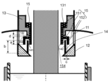
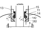
図1は、本発明の単結晶製造装置の一例を示す概略断面図である。図2は、図1に示した単結晶製造装置の一例における、冷却補助筒周辺部の拡大概略断面図である。 FIG. 1 is a schematic cross-sectional view showing an example of a single crystal manufacturing apparatus of the present invention. FIG. 2 is an enlarged schematic cross-sectional view of the vicinity of the cooling auxiliary tube in the example of the single crystal manufacturing apparatus shown in FIG.
図1及び図2に示す単結晶製造装置1は、天井部21を備え、シリコン融液6を収容する石英ルツボ7及びこれを支持する黒鉛ルツボ8を格納するメインチャンバ2と、メインチャンバ2の上部に不図示のゲートバルブを介して連設された引き上げチャンバ3と、シリコン融液6と対向するように配置された熱遮蔽部材12と、熱遮蔽部材12上に配置された整流筒14と、メインチャンバ2の天井部21からシリコン融液6に向かって延伸した部分131を含む冷却筒13と、冷却筒13の内側に嵌合された冷却補助筒15とを有する。
The single crystal manufacturing apparatus 1 shown in FIGS. 1 and 2 includes a
メインチャンバ2は、黒鉛ルツボ8を支持するルツボサポート16と、ルツボサポート16を支持したルツボ軸17と、黒鉛ルツボ8を取り囲むように配置されたヒーター9と、ヒーター9を取り囲むように配置された断熱材10とを更に格納している。ルツボ軸17は、シリコン融液6、石英ルツボ7、黒鉛ルツボ8及びルツボサポート16を、回転軸18を中心として自転させることができると共に、これらを昇降させることができる。
The
メインチャンバ2の天井部21には、筒部11が配置されている。筒部11は、天井部21からシリコン融液6に向けて延伸しており、端部に熱遮蔽部材12が取り付けられている。
A
引き上げチャンバ3は、シリコン融液6から引き上げられたシリコン単結晶5を収容するものである。
The pulling chamber 3 accommodates the silicon
整流筒14は、熱遮蔽部材12とは逆側の上端部141を含む。整流筒14は、引き上げ中のシリコン単結晶5を包囲するように、熱遮蔽部材12上に配置されている。図1及び図2に示した例では、整流筒14は、メインチャンバ2内に配置されている。
The straightening
冷却筒13は、引き上げ中のシリコン単結晶5を取り囲むように配置されている。また、冷却筒13のうちの一部131は、メインチャンバ2の天井部21からシリコン融液6に向かって延伸している。この部分131は、メインチャンバ2内に配置されており、シリコン融液6に対面する底面132を有している。また、冷却筒13は、不図示のゲートバルブ直下に位置するメインチャンバ2の天井部21から上方に延出したメインチャンバ上端部の内側に嵌合された部分133を更に含んでいる。冷却筒13は、不図示の冷却媒体循環機構によって供給される冷却媒体により、強制冷却されるものである。
Cooling
冷却補助筒15は、第1部分151と、第2部分152とを有している。冷却補助筒15の第1部分151は、図1及び図2に示すように、冷却筒13の底面132を囲繞している。より詳細には、冷却補助筒15の第1部分151は、冷却筒13の底面132を含む一部131を上下方向及び一方の側面から囲繞している。冷却補助筒15の第1部分151は、図2に示す、シリコン単結晶5の引き上げ方向に対して略垂直な方向に延伸する鍔部153を含む。
The
一方、冷却補助筒15の第2部分152は、図1及び図2に示すように、メインチャンバ2内で、整流筒14の上端部141を囲繞している。より詳細には、冷却補助筒15の第2部分152は、図2に示した溝部154を含む。溝部154は、整流筒14の上端部141を収容し、それにより、整流筒14の側面142の一部を覆っている。また、冷却補助筒15の第1部分151の鍔153も、第2部分152の一部である溝部154の底部として、整流筒14の上端部141を囲繞している。
On the other hand, the
冷却補助筒15の第1部分151(より具体的には鍔部153)と、冷却筒13の底面132との間隙は、図2に示す「d」で表される。間隙dは、1.0mm以下であることが好ましい。また、整流筒14の側面142の全面積のうち冷却補助筒15の溝部154で覆われた領域の割合は、図2に示す「a」及び「b」を用いると、「(a/b)×100」で表される。比a/bは、10%以上35%以下であることが好ましい。そして、冷却補助筒15の第2部分152の溝部154における冷却補助筒15と整流筒14の側面142との間隙は、図2に示す「c」で表される。間隙cは、5mm以上25mm以下であることが好ましい。なお、上記aは周方向の平均値である。一方、上記b~dは、全周方向にわたってほぼ一定の値であることが好ましい。そのため、比a/bは、周方向の平均値であることが好ましい。
The gap between the first portion 151 (more specifically, the collar portion 153) of the
以上では、整流筒14の側面142に開口部がない場合を説明したが、例えば図3に示すように、整流筒14の側面142には開口部143が設けられていてもよい。
In the above, a case has been described in which there is no opening in the
図3に示すような側面142に開口部143を有する整流筒14を用いることで、整流筒14の開口部143から筒部11にある炉内監視用窓の方向に流れる不活性ガスの流速が上昇し、その結果として、筒部11の内部や筒部11の外側から炭素含有ガスがシリコン融液6側により逆流しにくくなる効果が得られる。
By using the straightening
図3に示す開口部143は、整流筒14の側面142の円周方向に等間隔で形成されている。
The
開口部143は、例えば角度0°、120°及び240°の3つの軸上に設けることができる。さらに、開口部143は、開口部143上端から下端までの長さを50mm以下とし、かつ、整流筒14の側面142の全面積の15%以下の領域を開口した構造とすることが好ましい。開口部143の開口した領域の、整流筒14の側面142の全面積に対する割合は、図3に示す開口部面積eの全面積fに対する割合、すなわち比e/fに対応する。
The
加えて、前記整流筒14の開口部143は、開口部上端の高さが整流筒14の全高の35%以下の高さに位置し、かつ、開口部の中心は整流筒14の下端部からの高さ30mm以上40mm以下の位置に設けた構造とすることが好ましい。
In addition, the
このような側面142に開口部143を有する整流筒14を用いることで、整流筒14の開口部143から筒部11にある炉内監視用窓の方向に流れる不活性ガスの流速が上昇し、その結果として、筒部11の内部や筒部11の外側から炭素含有ガスがシリコン融液6側に更に逆流しにくくなる効果が得られる。
By using the straightening
次に、本発明の単結晶製造装置を用いた単結晶製造方法の例を、図1及び図2を参照しながら説明する。ただし、本発明の単結晶製造装置は、図1及び図2に示した単結晶製造装置には限定されないし、本発明の単結晶製造装置を用いた単結晶製造方法は、以下に例示するものに限定されない。 Next, an example of a single crystal manufacturing method using the single crystal manufacturing apparatus of the present invention will be described with reference to FIGS. 1 and 2. However, the single crystal manufacturing apparatus of the present invention is not limited to the single crystal manufacturing apparatus shown in FIGS. 1 and 2, and the single crystal manufacturing method using the single crystal manufacturing apparatus of the present invention is exemplified below. but not limited to.
まず、種結晶4をシリコン融液6に浸漬し、種結晶4と石英ルツボ7及び黒鉛ルツボ8とを回転軸18を中心に自転させながら種結晶4を静かに上方に引上げて棒状のシリコン単結晶5を成長させる一方、所望の直径と結晶品質を得るため融液面の高さが常に一定に保たれるように結晶の成長に合わせて石英ルツボ7及び黒鉛ルツボ8を上昇させる。石英ルツボ7及び黒鉛ルツボ8の上昇、並びに石英ルツボ7及び黒鉛ルツボ8の回転は、ルツボ軸17を用いて行うことができる。
First, the
シリコン融液6は、石英ルツボ7内に原料シリコンを投入し、この原料シリコンをヒーター9を用いて溶融させることによって得ることができる。
The
このとき使用する原料シリコンは、半導体グレードの高純度原料であることが好ましい。本発明は、冷却補助筒15の第1部分151によって冷却筒13の底面132を囲繞し且つ第2部分152によって整流筒14の上端部141を覆う構造を採用することで結晶製造プロセスに起因した炭素の汚染を低減する技術であるが、高純度の原料を使用することにより、原料からの持ち込みによる汚染量を低減でき、それにより、炭素濃度が低い単結晶をより確実に製造することができる。よって、使用する原料シリコンは半導体グレードの高純度原料であることが好ましい。
The raw material silicon used at this time is preferably a semiconductor grade high purity raw material. The present invention originates from the crystal manufacturing process by adopting a structure in which the
図1及び図2に示す単結晶製造装置1の一例を用いることにより、冷却筒13に、シリコン単結晶5からの輻射熱やヒーター9等の高温部からの輻射熱を十分に伝えることができ、伝わった熱を、冷却媒体による強制冷却で除去できる。それにより、シリコン単結晶をより効率的に製造できる。
By using the example of the single crystal manufacturing apparatus 1 shown in FIGS. 1 and 2, the radiant heat from the silicon
そして、図1及び図2に示す単結晶製造装置1の一例では、冷却補助筒15の周りの、例えばシリコン融液直上のシリコン単結晶5の周りの空間や、冷却補助筒15と筒部11とで囲まれた空間の温度を低下させることができる。それにより、製造装置1内の炭素部材とシリコン融液6から蒸発するSiOとの反応を抑制でき、ひいては炭素含有ガスの発生を抑制できる。加えて、上記反応が起きて炭素含有ガスが生じても、上端部141が冷却補助筒15の第2部分152に囲繞された整流筒14により、この炭素含有ガスがシリコン融液に逆流するのを防ぐことができる。
In the example of the single crystal manufacturing apparatus 1 shown in FIGS. 1 and 2, the space around the
すなわち、図1及び図2に示す単結晶製造装置1の一例を用いれば、炭素濃度が低い単結晶を効率よく製造することができる。 That is, by using an example of the single crystal manufacturing apparatus 1 shown in FIGS. 1 and 2, a single crystal with a low carbon concentration can be efficiently manufactured.
また、図1及び図2に示す単結晶製造装置1の一例において、整流筒14を、図3に示すような側面142に開口部143を有するものとすることで、先に説明したように、炭素含有ガスがシリコン融液6側に逆流するのを更に防ぐことができる。
Furthermore, in the example of the single crystal manufacturing apparatus 1 shown in FIGS. 1 and 2, the rectifying
以下、実施例及び比較例を用いて本発明を具体的に説明するが、本発明はこれらに限定されるものではない。 Hereinafter, the present invention will be specifically explained using Examples and Comparative Examples, but the present invention is not limited thereto.
各実施例及び比較例では、以下に説明する単結晶製造装置を用いて、以下の共通条件で、単結晶の製造を行なった。ルツボとして、口径81.28cm(32インチ)を用いた。このルツボに360kgの原料シリコンを入れて、これをヒーターで溶融して、シリコン融液を得た。シリコン融液に水平磁場を印加しながら、結晶直径300mmの結晶の引き上げを行った。引き上げ後の直径300mmの結晶について、各直胴位置からサンプルを切り出し、PL法を用いて炭素濃度の定量を実施した。 In each Example and Comparative Example, a single crystal was manufactured under the following common conditions using the single crystal manufacturing apparatus described below. A crucible with a diameter of 81.28 cm (32 inches) was used. 360 kg of raw silicon was put into this crucible and melted with a heater to obtain a silicon melt. A crystal with a crystal diameter of 300 mm was pulled while applying a horizontal magnetic field to the silicon melt. Samples were cut out from each straight body position of the crystal with a diameter of 300 mm after being pulled, and the carbon concentration was determined using the PL method.
(実施例1)
実施例1では、図1及び図2を参照しながら説明した単結晶製造装置1と同様の構造を有する単結晶製造装置を用いた。すなわち、実施例1では、引き上げ中のシリコン単結晶5を同芯に包囲するように、熱遮蔽部材12上に整流筒14を配置し、冷却補助筒15の下部である第2部分152によって整流筒14の上端部141を覆う構造の冷却補助筒15を用いて単結晶の製造を行った。なお、このときの整流筒14の材質は合成石英とし、冷却補助筒15の材質は、熱伝導率が金属と比較して同等以上であり、かつ輻射率が金属より高い黒鉛材を使用した。また、用いた整流筒14は、図1及び図2に示すように、側面に開口部のない(図3における比e/f=0%)、全閉構造の整流筒であった。
(Example 1)
In Example 1, a single crystal manufacturing apparatus having the same structure as the single crystal manufacturing apparatus 1 described with reference to FIGS. 1 and 2 was used. That is, in Example 1, the rectifying
図2に示す通り、整流筒上部の冷却補助筒で覆われている部分の面積と整流筒側面の全面積の比をa/b、冷却補助筒下部にある溝部の側面と整流筒側面の間隔をc、冷却補助筒と前記冷却筒の底面の間隙をdとし、実施例1では、a/b=35%、c=5mmに固定して、d=0mm(完全接触)、d=1.0mm、d=3.0mmの3水準を用意して単結晶の製造を行った。 As shown in Figure 2, the ratio of the area of the part covered by the auxiliary cooling tube at the top of the straightening tube to the total area of the side surface of the straightening tube is a/b, and the distance between the side surface of the groove at the bottom of the auxiliary cooling tube and the side surface of the straightening tube. is c, the gap between the cooling auxiliary cylinder and the bottom surface of the cooling cylinder is d, and in Example 1, a/b=35%, c=5 mm, d=0 mm (complete contact), d=1. Single crystals were manufactured using three levels: 0 mm and d=3.0 mm.
(比較例1)
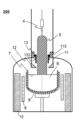
比較例1では、図8に示すような構造を有する単結晶製造装置を用いた。すなわち、比較例1では、熱遮蔽部材12の上に整流筒を搭載せずに、冷却筒13のシリコン融液6に対面する底面132を覆う構造を有していない冷却補助筒115を用いる点で実施例1の単結晶製造装置と異なる単結晶製造装置を用いて単結晶の製造を行った。
(Comparative example 1)
In Comparative Example 1, a single crystal manufacturing apparatus having a structure as shown in FIG. 8 was used. That is, in Comparative Example 1, the straightening tube is not mounted on the
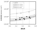
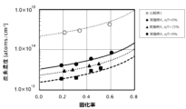
実施例1及び比較例1の結果を図4に示す。本発明に係る単結晶製造装置を用いた実施例1では、図8のような比較例1の製造装置を用いて製造を行った場合に比べて、いずれの固化率においても炭素濃度の低い単結晶を得ることができたことが分かる。特に、実施例1において冷却補助筒と冷却筒底面との間隙dが0mm(完全接触)の場合では、比較例1の製造装置を用いて製造を行った場合に比べて、単結晶中の炭素濃度が89%程度減少するという結果が得られた。また、図4から判るように、実施例1の冷却補助筒と冷却筒底面の間隙dが1mm以下であれば比較例1に比べて単結晶中の炭素濃度を顕著に減少できることが確認できている。このため、本発明で用いる製造装置の冷却補助筒と冷却筒底面の間隙dは1mm以下とすることが好ましい。一方で、実施例1の冷却補助筒と冷却筒の底面の間隙dを3mmとしても、比較例1の場合と比べて単結晶中の炭素濃度が77%程度減少するという結果が得られた。 The results of Example 1 and Comparative Example 1 are shown in FIG. In Example 1 using the single crystal manufacturing apparatus according to the present invention, a single crystal with a lower carbon concentration was produced at any solidification rate compared to the case of manufacturing using the manufacturing apparatus of Comparative Example 1 as shown in FIG. It turns out that we were able to obtain crystals. In particular, when the gap d between the cooling auxiliary cylinder and the bottom surface of the cooling cylinder was 0 mm (complete contact) in Example 1, the carbon in the single crystal was The result was that the concentration was reduced by about 89%. Furthermore, as can be seen from FIG. 4, it was confirmed that if the gap d between the auxiliary cooling cylinder and the bottom of the cooling cylinder in Example 1 was 1 mm or less, the carbon concentration in the single crystal could be significantly reduced compared to Comparative Example 1. There is. Therefore, it is preferable that the gap d between the cooling auxiliary cylinder and the bottom surface of the cooling cylinder in the manufacturing apparatus used in the present invention is 1 mm or less. On the other hand, even if the gap d between the cooling auxiliary cylinder and the bottom surface of the cooling cylinder in Example 1 was set to 3 mm, the result was that the carbon concentration in the single crystal was reduced by about 77% compared to Comparative Example 1.
(実施例2)
実施例2では、図2のc=5mm、d=1.0mmに固定して、a/b=10%、a/b=35%の2水準のそれぞれを満たす単結晶製造装置を用意して単結晶の製作を行った。なお、実施例2でも、実施例1と同様、用いた整流筒14は、図1及び図2に示すように、側面に開口部のない(図3における比e/f=0%)、全閉構造の整流筒であった。
(Example 2)
In Example 2, a single-crystal manufacturing apparatus was prepared that satisfied the two levels of a/b = 10% and a/b = 35% by fixing c = 5 mm and d = 1.0 mm in Fig. 2. A single crystal was produced. In Example 2, as in Example 1, the
(比較例2)
比較例2では、a/b=0%とした、すなわち整流筒14の上端部141が冷却補助筒15の第2部分152で囲繞されていない点以外は実施例2で用いたのと同様の単結晶製造装置を用いて単結晶の製作を行なった。
(Comparative example 2)
Comparative Example 2 was the same as that used in Example 2 except that a/b = 0%, that is, the
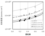
実施例2、比較例1及び比較例2の結果を図5に示す。本発明に係る単結晶製造装置を用いた実施例2では、図8のような比較例1の製造装置を用いて製造を行った場合に比べて、いずれの固化率においても炭素濃度の低い単結晶を得ることができたことが分かる。特に、実施例2において整流筒14の上端部141の冷却補助筒で覆われている部分の面積と整流筒141の側面142の全面積の比a/bを35%とした場合、比較例1の製造装置を用いて製造を行った場合に比べて、単結晶中の炭素濃度が85%程度減少するという結果が得られた。また、図5から判るように、実施例2のa/bが10%以上であれば比較例1及び2に比べて単結晶中の炭素濃度が顕著に減少することが確認できている。このため、本発明で用いる製造装置の整流筒14の上端部141の冷却補助筒15で覆われている部分の面積と整流筒14の側面142の全面積の比の下限値は10%とすることが好ましい。一方で、a/b=0%とした比較例2では、比較例1の場合と比べて単結晶中の炭素濃度が67%程度減少するという結果が得られているが、実施例2の結果に比べると不十分であった。
The results of Example 2, Comparative Example 1, and Comparative Example 2 are shown in FIG. In Example 2 using the single crystal manufacturing apparatus according to the present invention, a single crystal with a lower carbon concentration was produced at any solidification rate compared to the case of manufacturing using the manufacturing apparatus of Comparative Example 1 as shown in FIG. It turns out that we were able to obtain crystals. In particular, when the ratio a/b of the area of the portion of the
なお、実施例2とは別に、a/b=40%となるような構造の冷却補助筒15を用いて単結晶の製造を行った。a/bを35%以下とした実施例2では、a/bを40%とした場合に比べ、直径測定用のカメラのための視野が確保しやすかった。この点を踏まえると、整流筒14の上端部141の冷却補助筒15で覆われている部分の面積の整流筒14の側面142の全面積に対する比の上限を35%とすることが好ましいことが分かる。
Note that, separately from Example 2, a single crystal was manufactured using a cooling
(実施例3)
実施例3では、a/b=35%、d=1.0mmに固定して、c=5mm、c=25mmの2水準のそれぞれを満たす単結晶製造装置を用意して単結晶の製作を行った。なお、実施例3でも、実施例1と同様、用いた整流筒14は、図1及び図2に示すように、側面に開口部のない(図3における比e/f=0%)、全閉構造の整流筒であった。
(Example 3)
In Example 3, a single crystal was manufactured by fixing a/b = 35% and d = 1.0 mm, and preparing a single crystal manufacturing apparatus that satisfies the two standards of c = 5 mm and c = 25 mm. Ta. In addition, in Example 3, as in Example 1, the rectifying
実施例3及び比較例1の結果を図6に示す。本発明に係る単結晶製造装置を用いた実施例3では、図8のような比較例1の製造装置を用いて製造を行った場合に比べて、いずれの固化率においても炭素濃度の低い単結晶を得ることができたことが分かる。特に、実施例3において、冷却補助筒15の溝部154側面と整流筒14側面142との間隔cを5mmとした場合は、比較例1の単結晶製造装置を用いて単結晶の製造を行った場合に比べて、単結晶中の炭素濃度が85%程度減少するという結果が得られた。また、図6から判るように、実施例3のcが25mm以下であれば比較例1に比べて単結晶中の炭素濃度が減少することが確認できている。
The results of Example 3 and Comparative Example 1 are shown in FIG. In Example 3 using the single crystal manufacturing apparatus according to the present invention, a single crystal with a lower carbon concentration was produced at any solidification rate compared to the case of manufacturing using the manufacturing apparatus of Comparative Example 1 as shown in FIG. It turns out that we were able to obtain crystals. In particular, in Example 3, when the distance c between the side surface of the
(実施例4)
整流筒14の側面142の開口部143の開口部面積eと整流筒14の側面142の全面積fの比をe/f(図3に示す)とし、実施例4では、a/b=35%、d=1.0mm、c=5mmに固定して、e/f=0%(全閉構造の整流筒)、e/f=9%、e/f=15%の3水準のそれぞれを満たす単結晶製造装置を用意して単結晶の製造を行った。なお、e/f=9%、e/f=15%の整流筒14は角度0°,120°,240°の3つの軸上に開口部143を設けた構造となっている。
(Example 4)
The ratio of the opening area e of the
上記の条件に加えて、e/f=9%の整流筒14では、開口部143の上端の高さが整流筒14の全高の24%の高さに位置しており、前記開口部143は開口部143の上端から下端までの長さ30mmの領域を開口した構造とした。
In addition to the above conditions, in the straightening
上記の条件に加えて、e/f=15%の整流筒14では、開口部143の上端の高さが整流筒14の全高の35%の高さに位置しており、前記開口部143は開口部143の上端から下端までの長さ50mmの領域を開口した構造とした。
In addition to the above conditions, in the straightening
実施例4及び比較例1の結果を図7に示す。本発明に係る単結晶製造装置を用いた実施例4のうち、整流筒14の側面142の開口部143の開口部面積eと整流筒14側面142の全面積fとの比e/fを9%とした場合は、図8のような従来構造の製造装置を用いて単結晶の製造を行った比較例1と比べて、単結晶中の炭素濃度が93%程度減少するという結果が得られた。また、図7から判るように、実施例4のe/fが0%を超え15%以下であれば比較例1に比べて単結晶中の炭素濃度が顕著に減少することが確認できている。
The results of Example 4 and Comparative Example 1 are shown in FIG. In Example 4 using the single crystal manufacturing apparatus according to the present invention, the ratio e/f of the opening area e of the
また、図7から、比e/fを9%又は15%とした場合は、e/f=0%(全閉構造の整流筒)とした場合に比べて単結晶中の炭素濃度が減少しており、整流筒14の側面142を開口したことによる効果で単結晶中の炭素濃度が更に減少することが確認できている。
Also, from Figure 7, when the ratio e/f is set to 9% or 15%, the carbon concentration in the single crystal decreases compared to when e/f is set to 0% (totally closed rectifier structure). It has been confirmed that the effect of opening the
なお、本発明は、上記実施形態に限定されるものではない。上記実施形態は例示であり、本発明の特許請求の範囲に記載された技術的思想と実質的に同一な構成を有し、同様な作用効果を奏するものは、いかなるものであっても本発明の技術的範囲に包含される。 Note that the present invention is not limited to the above embodiments. The above-mentioned embodiments are illustrative, and any embodiment that has substantially the same configuration as the technical idea stated in the claims of the present invention and has similar effects is the present invention. covered within the technical scope of.
1、200…単結晶製造装置、 2…メインチャンバ、 21…天井部、 3…引き上げチャンバ、 4…種結晶、 5…シリコン単結晶、 6…シリコン融液、 7…石英ルツボ、 8…黒鉛ルツボ、 9…ヒーター、 10…断熱材、 11…筒部、12…熱遮蔽部材、 13…冷却筒、 131、133…冷却筒の一部、 132…底面、 14…整流筒、 141…上端部、 142…側面、 143…開口部、 15、115…冷却補助筒、 151…第1部分、 152…第2部分、 153…鍔部、 154…溝部、 16…ルツボサポート、 17…ルツボ軸、 18…回転軸。
DESCRIPTION OF
Claims (6)
天井部を備え、シリコン融液を収容するルツボを格納するメインチャンバと、
前記メインチャンバの前記天井部からゲートバルブを介して上方に連設し、前記シリコン融液から引き上げられたシリコン単結晶を収容する引き上げチャンバと、
前記ルツボに収容された前記シリコン融液と対向するように配置された熱遮蔽部材と、
引き上げ中の前記シリコン単結晶を包囲するように前記熱遮蔽部材上に配置された整流筒と、
引き上げ中の前記シリコン単結晶を取り囲むように配置され、前記メインチャンバの前記天井部から前記シリコン融液に向かって延伸した部分を含み、冷却媒体で強制冷却される冷却筒と、
前記冷却筒の内側に嵌合された冷却補助筒と
を有し、
前記冷却筒の前記延伸した部分は、前記シリコン融液に対面する底面を有し、
前記冷却補助筒は、少なくとも、前記冷却筒の前記底面を囲繞した第1部分と、前記整流筒の上端部を囲繞した第2部分とを有するものであることを特徴とする単結晶製造装置。 A single crystal manufacturing device for growing a single crystal by the Czochralski method,
a main chamber having a ceiling and housing a crucible containing silicon melt;
a pulling chamber connected upwardly from the ceiling of the main chamber via a gate valve and accommodating a silicon single crystal pulled from the silicon melt;
a heat shielding member disposed to face the silicon melt contained in the crucible;
a rectifier cylinder disposed on the heat shielding member so as to surround the silicon single crystal being pulled;
a cooling cylinder arranged to surround the silicon single crystal being pulled, including a portion extending from the ceiling of the main chamber toward the silicon melt, and forcedly cooled with a cooling medium;
and a cooling auxiliary cylinder fitted inside the cooling cylinder,
The extended portion of the cooling cylinder has a bottom surface facing the silicon melt,
The auxiliary cooling cylinder is characterized in that it has at least a first part surrounding the bottom surface of the cooling cylinder and a second part surrounding the upper end of the straightening cylinder.
前記冷却補助筒の前記第1部分は、前記冷却筒の前記底面を覆う構造を有し、前記冷却補助筒の前記第1部分と前記冷却筒の前記底面との間隙が1.0mm以下のものであることを特徴とする請求項1又は請求項2に記載の単結晶製造装置。 The cooling auxiliary cylinder is made of at least one member selected from the group consisting of graphite member, carbon composite member, stainless steel, molybdenum, and tungsten,
The first portion of the auxiliary cooling tube has a structure that covers the bottom surface of the cooling tube, and the gap between the first portion of the auxiliary cooling tube and the bottom surface of the cooling tube is 1.0 mm or less. The single crystal manufacturing apparatus according to claim 1 or 2, characterized in that:
Priority Applications (5)
| Application Number | Priority Date | Filing Date | Title |
|---|---|---|---|
| JP2020205263A JP7420060B2 (en) | 2020-12-10 | 2020-12-10 | Single crystal manufacturing equipment |
| US18/037,802 US12454767B2 (en) | 2020-12-10 | 2021-11-01 | Single crystal manufacturing apparatus |
| PCT/JP2021/040259 WO2022123957A1 (en) | 2020-12-10 | 2021-11-01 | Monocrystal-manufacturing device |
| KR1020237018918A KR102900919B1 (en) | 2020-12-10 | 2021-11-01 | Single crystal manufacturing equipment |
| DE112021005336.1T DE112021005336T5 (en) | 2020-12-10 | 2021-11-01 | DEVICE FOR THE PRODUCTION OF A MONOCRYSTAL |
Applications Claiming Priority (1)
| Application Number | Priority Date | Filing Date | Title |
|---|---|---|---|
| JP2020205263A JP7420060B2 (en) | 2020-12-10 | 2020-12-10 | Single crystal manufacturing equipment |
Publications (2)
| Publication Number | Publication Date |
|---|---|
| JP2022092442A JP2022092442A (en) | 2022-06-22 |
| JP7420060B2 true JP7420060B2 (en) | 2024-01-23 |
Family
ID=82068147
Family Applications (1)
| Application Number | Title | Priority Date | Filing Date |
|---|---|---|---|
| JP2020205263A Active JP7420060B2 (en) | 2020-12-10 | 2020-12-10 | Single crystal manufacturing equipment |
Country Status (1)
| Country | Link |
|---|---|
| JP (1) | JP7420060B2 (en) |
Citations (2)
| Publication number | Priority date | Publication date | Assignee | Title |
|---|---|---|---|---|
| WO2001057293A1 (en) | 2000-01-31 | 2001-08-09 | Shin-Etsu Handotai Co., Ltd. | Single crystal growing device and production method of single crystal using the device and single crystal |
| JP2020152612A (en) | 2019-03-20 | 2020-09-24 | 信越半導体株式会社 | Single crystal manufacturing equipment |
-
2020
- 2020-12-10 JP JP2020205263A patent/JP7420060B2/en active Active
Patent Citations (2)
| Publication number | Priority date | Publication date | Assignee | Title |
|---|---|---|---|---|
| WO2001057293A1 (en) | 2000-01-31 | 2001-08-09 | Shin-Etsu Handotai Co., Ltd. | Single crystal growing device and production method of single crystal using the device and single crystal |
| JP2020152612A (en) | 2019-03-20 | 2020-09-24 | 信越半導体株式会社 | Single crystal manufacturing equipment |
Also Published As
| Publication number | Publication date |
|---|---|
| JP2022092442A (en) | 2022-06-22 |
Similar Documents
| Publication | Publication Date | Title |
|---|---|---|
| US9068277B2 (en) | Apparatus for manufacturing single-crystal silicon carbide | |
| JP5904079B2 (en) | Silicon single crystal growing apparatus and silicon single crystal growing method | |
| CN103282558B (en) | The manufacture method of the manufacturing installation of SiC monocrystal, the fixture used in the manufacturing apparatus and SiC monocrystal | |
| US4597949A (en) | Apparatus for growing crystals | |
| KR101105950B1 (en) | Monocrystalline Ingot Manufacturing Equipment | |
| JP4097729B2 (en) | Semiconductor single crystal manufacturing equipment | |
| JP2005179080A (en) | Single crystal manufacturing method and manufacturing apparatus | |
| EP0903427B1 (en) | Apparatus and method for producing crystals by the czochralski method and crystals produced by this method | |
| KR102900919B1 (en) | Single crystal manufacturing equipment | |
| JP7420060B2 (en) | Single crystal manufacturing equipment | |
| CN111286785A (en) | Crystal growth device and crucible | |
| JP5392040B2 (en) | Single crystal manufacturing apparatus and single crystal manufacturing method | |
| JP7501340B2 (en) | Single crystal manufacturing equipment | |
| KR101756687B1 (en) | Single crystal manufacturing device and single crystal manufacturing method | |
| JP4053125B2 (en) | Method for synthesizing SiC single crystal | |
| JP7115592B1 (en) | Single crystal manufacturing equipment | |
| JP2009292684A (en) | Silicon single crystal production method and production apparatus therefore | |
| JP3498330B2 (en) | Single crystal growth equipment | |
| JPWO2002036861A1 (en) | Apparatus and method for producing silicon semiconductor single crystal | |
| JP3812573B2 (en) | Semiconductor crystal growth method | |
| KR100468117B1 (en) | Production method for high-quality silicon single crystal | |
| JP4155085B2 (en) | Method for producing compound semiconductor single crystal | |
| JP2007210820A (en) | Method for producing silicon single crystal | |
| JPH06305878A (en) | Apparatus for producing silicon single crystal | |
| JP2013193942A (en) | Single crystal manufacturing apparatus and method for manufacturing single crystal using the same |
Legal Events
| Date | Code | Title | Description |
|---|---|---|---|
| A521 | Request for written amendment filed |
Free format text: JAPANESE INTERMEDIATE CODE: A523 Effective date: 20211101 |
|
| A621 | Written request for application examination |
Free format text: JAPANESE INTERMEDIATE CODE: A621 Effective date: 20221121 |
|
| TRDD | Decision of grant or rejection written | ||
| A01 | Written decision to grant a patent or to grant a registration (utility model) |
Free format text: JAPANESE INTERMEDIATE CODE: A01 Effective date: 20231212 |
|
| A61 | First payment of annual fees (during grant procedure) |
Free format text: JAPANESE INTERMEDIATE CODE: A61 Effective date: 20231225 |
|
| R150 | Certificate of patent or registration of utility model |
Ref document number: 7420060 Country of ref document: JP Free format text: JAPANESE INTERMEDIATE CODE: R150 |