JP7433863B2 - 光電変換装置、撮像システム、および移動体 - Google Patents
光電変換装置、撮像システム、および移動体 Download PDFInfo
- Publication number
- JP7433863B2 JP7433863B2 JP2019214776A JP2019214776A JP7433863B2 JP 7433863 B2 JP7433863 B2 JP 7433863B2 JP 2019214776 A JP2019214776 A JP 2019214776A JP 2019214776 A JP2019214776 A JP 2019214776A JP 7433863 B2 JP7433863 B2 JP 7433863B2
- Authority
- JP
- Japan
- Prior art keywords
- photoelectric conversion
- well
- signal
- pixel
- transistor
- Prior art date
- Legal status (The legal status is an assumption and is not a legal conclusion. Google has not performed a legal analysis and makes no representation as to the accuracy of the status listed.)
- Active
Links
Images




Classifications
-
- H—ELECTRICITY
- H10—SEMICONDUCTOR DEVICES; ELECTRIC SOLID-STATE DEVICES NOT OTHERWISE PROVIDED FOR
- H10F—INORGANIC SEMICONDUCTOR DEVICES SENSITIVE TO INFRARED RADIATION, LIGHT, ELECTROMAGNETIC RADIATION OF SHORTER WAVELENGTH OR CORPUSCULAR RADIATION
- H10F39/00—Integrated devices, or assemblies of multiple devices, comprising at least one element covered by group H10F30/00, e.g. radiation detectors comprising photodiode arrays
- H10F39/80—Constructional details of image sensors
- H10F39/803—Pixels having integrated switching, control, storage or amplification elements
-
- H—ELECTRICITY
- H10—SEMICONDUCTOR DEVICES; ELECTRIC SOLID-STATE DEVICES NOT OTHERWISE PROVIDED FOR
- H10F—INORGANIC SEMICONDUCTOR DEVICES SENSITIVE TO INFRARED RADIATION, LIGHT, ELECTROMAGNETIC RADIATION OF SHORTER WAVELENGTH OR CORPUSCULAR RADIATION
- H10F30/00—Individual radiation-sensitive semiconductor devices in which radiation controls the flow of current through the devices, e.g. photodetectors
- H10F30/20—Individual radiation-sensitive semiconductor devices in which radiation controls the flow of current through the devices, e.g. photodetectors the devices having potential barriers, e.g. phototransistors
- H10F30/21—Individual radiation-sensitive semiconductor devices in which radiation controls the flow of current through the devices, e.g. photodetectors the devices having potential barriers, e.g. phototransistors the devices being sensitive to infrared, visible or ultraviolet radiation
-
- H—ELECTRICITY
- H10—SEMICONDUCTOR DEVICES; ELECTRIC SOLID-STATE DEVICES NOT OTHERWISE PROVIDED FOR
- H10F—INORGANIC SEMICONDUCTOR DEVICES SENSITIVE TO INFRARED RADIATION, LIGHT, ELECTROMAGNETIC RADIATION OF SHORTER WAVELENGTH OR CORPUSCULAR RADIATION
- H10F39/00—Integrated devices, or assemblies of multiple devices, comprising at least one element covered by group H10F30/00, e.g. radiation detectors comprising photodiode arrays
- H10F39/80—Constructional details of image sensors
- H10F39/803—Pixels having integrated switching, control, storage or amplification elements
- H10F39/8037—Pixels having integrated switching, control, storage or amplification elements the integrated elements comprising a transistor
-
- H—ELECTRICITY
- H10—SEMICONDUCTOR DEVICES; ELECTRIC SOLID-STATE DEVICES NOT OTHERWISE PROVIDED FOR
- H10F—INORGANIC SEMICONDUCTOR DEVICES SENSITIVE TO INFRARED RADIATION, LIGHT, ELECTROMAGNETIC RADIATION OF SHORTER WAVELENGTH OR CORPUSCULAR RADIATION
- H10F77/00—Constructional details of devices covered by this subclass
- H10F77/95—Circuit arrangements
- H10F77/953—Circuit arrangements for devices having potential barriers
-
- B—PERFORMING OPERATIONS; TRANSPORTING
- B60—VEHICLES IN GENERAL
- B60R—VEHICLES, VEHICLE FITTINGS, OR VEHICLE PARTS, NOT OTHERWISE PROVIDED FOR
- B60R11/00—Arrangements for holding or mounting articles, not otherwise provided for
- B60R11/04—Mounting of cameras operative during drive; Arrangement of controls thereof relative to the vehicle
Landscapes
- Solid State Image Pick-Up Elements (AREA)
- Transforming Light Signals Into Electric Signals (AREA)
- Metal-Oxide And Bipolar Metal-Oxide Semiconductor Integrated Circuits (AREA)
Description
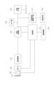
図1~図5を用いて、本発明の実施形態1に係る光電変換装置について説明する。


図6、図7を用いて、本発明の実施形態2に係る画素について説明する。本実施形態は、画素が、複数のPD201と複数のTX203を含み、複数のPD201がFD202を共有している点が実施形態1とは異なる。以下、実施形態1と同様の構成は説明を省略し、異なる構成を中心に説明する。
図8~図10を用いて、本発明の実施形態3に係る画素について説明する。本実施形態は、複数のAMPがSELを共有している点が実施形態2とは異なる。以下、実施形態2と同様の構成は説明を省略し、異なる構成を中心に説明する。
図11、図12を用いて、本発明の実施形態4に係る画素について説明する。本実施形態は、1つの画素が2つの光電変換部PDを含む点が実施形態1とは異なる。以下、実施形態1と同様の構成は説明を省略し、異なる構成を中心に説明する。
図13は本実施形態における撮像システムのブロック図である。撮像システムは、デジタルスチルカメラ、デジタルカムコーダ、カメラヘッド、監視用カメラ、複写機、ファックス、携帯端末、スマートフォン、車載カメラ、観測衛星、人口知能ロボットなどであり得る。本実施形態における撮像装置1100は、実施形態1から実施形態4の光電変換装置である。
図14(A)、図14(B)は、実施形態1~実施形態4における光電変換装置を車戴カメラに関する撮像システムに適用した例を示している。本実施形態において、撮像装置2010は実施形態1~実施形態4の光電変換装置に相当する。
102 画素
201 光電変換部(PD)
202 浮遊拡散部(FD)
203 転送トランジスタ(TX)
204 リセットトランジスタ(RES)
205 選択トランジスタ(SEL)
206 増幅トランジスタ(AMP)
301 半導体基板
DTI 絶縁体分離部
WAMP AMPが配されるウェル
WPD PDが配されるウェル
Claims (9)
- 半導体基板と、
前記半導体基板内に設けられた光電変換部と、前記光電変換部で生成された信号キャリアが転送される浮遊拡散部と、前記光電変換部からの信号を出力する増幅トランジスタと、前記浮遊拡散部に接続されるリセットトランジスタと、前記増幅トランジスタと出力線とに接続される選択トランジスタと、
平面視で、前記増幅トランジスタを取り囲んで、前記光電変換部と前記増幅トランジスタとの間に配され、前記半導体基板を貫通する絶縁体分離部と、を備え、
前記増幅トランジスタが配される第1ウェルと、前記リセットトランジスタと前記選択トランジスタとが配される第2ウェルと、を有し、
前記第1ウェルと、前記増幅トランジスタのソースまたはドレインと、が接続されており、
前記絶縁体分離部は、前記増幅トランジスタと前記リセットトランジスタとの間に配されていることを特徴とする光電変換装置。 - 前記増幅トランジスタはソースフォロワトランジスタであり、
前記第1ウェルと前記増幅トランジスタのソースとが接続されていることを特徴とする請求項1に記載の光電変換装置。 - 前記光電変換部は、前記第2ウェルに配されており、
前記第2ウェルと前記第1ウェルとの間に前記絶縁体分離部が配されていることを特徴とする請求項1または2に記載の光電変換装置。 - 前記浮遊拡散部は、前記第2ウェルに配され、
前記増幅トランジスタと前記浮遊拡散部との間に前記絶縁体分離部が配されることを特徴とする請求項1乃至3のいずれか1項に記載の光電変換装置。 - 前記絶縁体分離部に囲まれた領域には、複数の前記増幅トランジスタが配されていることを特徴とする請求項1乃至4のいずれか1項に記載の光電変換装置。
- 前記選択トランジスタが前記複数の増幅トランジスタにより共有されることを特徴とする請求項5に記載の光電変換装置。
- 前記複数の増幅トランジスタにおいて、読み出しを行わない前記増幅トランジスタのゲートに印加する電圧は、読み出しを行う前記増幅トランジスタのゲートに印加する電圧よりも低いことを特徴とする請求項5または6に記載の光電変換装置。
- 請求項1乃至7のいずれか1項に記載の光電変換装置と、
前記光電変換装置から出力される信号を処理する信号処理部と、を有することを特徴とする撮像システム。 - 移動体であって、
請求項1乃至7のいずれか1項に記載の光電変換装置と、
前記光電変換装置からの信号に基づく視差画像から、対象物までの距離情報を取得する距離情報取得手段と、
前記距離情報に基づいて前記移動体を制御する制御手段と、を有することを特徴とする移動体。
Priority Applications (2)
| Application Number | Priority Date | Filing Date | Title |
|---|---|---|---|
| JP2019214776A JP7433863B2 (ja) | 2019-11-27 | 2019-11-27 | 光電変換装置、撮像システム、および移動体 |
| US17/103,160 US12068342B2 (en) | 2019-11-27 | 2020-11-24 | Photoelectric conversion device, imaging system, and movable body |
Applications Claiming Priority (1)
| Application Number | Priority Date | Filing Date | Title |
|---|---|---|---|
| JP2019214776A JP7433863B2 (ja) | 2019-11-27 | 2019-11-27 | 光電変換装置、撮像システム、および移動体 |
Publications (2)
| Publication Number | Publication Date |
|---|---|
| JP2021086919A JP2021086919A (ja) | 2021-06-03 |
| JP7433863B2 true JP7433863B2 (ja) | 2024-02-20 |
Family
ID=75975062
Family Applications (1)
| Application Number | Title | Priority Date | Filing Date |
|---|---|---|---|
| JP2019214776A Active JP7433863B2 (ja) | 2019-11-27 | 2019-11-27 | 光電変換装置、撮像システム、および移動体 |
Country Status (2)
| Country | Link |
|---|---|
| US (1) | US12068342B2 (ja) |
| JP (1) | JP7433863B2 (ja) |
Families Citing this family (2)
| Publication number | Priority date | Publication date | Assignee | Title |
|---|---|---|---|---|
| JP7336320B2 (ja) * | 2019-09-04 | 2023-08-31 | キヤノン株式会社 | 撮像装置及びその制御方法、プログラム、記憶媒体 |
| WO2024253074A1 (ja) * | 2023-06-09 | 2024-12-12 | ソニーセミコンダクタソリューションズ株式会社 | 光検出装置および電子機器 |
Citations (7)
| Publication number | Priority date | Publication date | Assignee | Title |
|---|---|---|---|---|
| JP2001160619A (ja) | 1999-12-01 | 2001-06-12 | Victor Co Of Japan Ltd | Cmosイメージセンサ及びその製造方法 |
| JP2010028423A (ja) | 2008-07-18 | 2010-02-04 | Sony Corp | 固体撮像素子およびカメラシステム |
| JP2011119441A (ja) | 2009-12-03 | 2011-06-16 | Sony Corp | 撮像素子およびカメラシステム |
| JP2013118273A (ja) | 2011-12-02 | 2013-06-13 | Sony Corp | 増幅回路および製造方法、撮像素子、並びに電子機器 |
| JP2016005068A (ja) | 2014-06-16 | 2016-01-12 | ソニー株式会社 | 固体撮像装置および電子機器 |
| JP2017183661A (ja) | 2016-03-31 | 2017-10-05 | キヤノン株式会社 | 光電変換装置およびカメラ |
| JP2019165136A (ja) | 2018-03-20 | 2019-09-26 | ソニーセミコンダクタソリューションズ株式会社 | 固体撮像装置およびその製造方法、並びに電子機器 |
Family Cites Families (30)
| Publication number | Priority date | Publication date | Assignee | Title |
|---|---|---|---|---|
| US6657665B1 (en) * | 1998-12-31 | 2003-12-02 | Eastman Kodak Company | Active Pixel Sensor with wired floating diffusions and shared amplifier |
| JP4003549B2 (ja) | 2001-06-28 | 2007-11-07 | 日本ビクター株式会社 | 固体撮像装置 |
| WO2006025079A1 (ja) * | 2004-07-20 | 2006-03-09 | Fujitsu Limited | Cmos撮像素子 |
| US7964929B2 (en) * | 2007-08-23 | 2011-06-21 | Aptina Imaging Corporation | Method and apparatus providing imager pixels with shared pixel components |
| US8115154B2 (en) * | 2008-08-01 | 2012-02-14 | Sony Corporation | Solid-state imaging device, method of producing the same, and imaging device |
| FR2950504B1 (fr) * | 2009-09-24 | 2012-06-22 | St Microelectronics Sa | Circuit de pixel de capteur d'image |
| FR2955701A1 (fr) * | 2010-01-28 | 2011-07-29 | St Microelectronics Sa | Structure compacte de capteur d'image |
| US9355888B2 (en) * | 2012-10-01 | 2016-05-31 | Taiwan Semiconductor Manufacturing Company, Ltd. | Implant isolated devices and method for forming the same |
| JP2015088621A (ja) | 2013-10-30 | 2015-05-07 | 株式会社東芝 | 固体撮像装置および固体撮像装置の製造方法 |
| KR102366416B1 (ko) * | 2014-08-11 | 2022-02-23 | 삼성전자주식회사 | Cmos 이미지 센서 |
| EP3343620A4 (en) * | 2015-09-29 | 2018-08-08 | Towerjazz Panasonic Semiconductor Co., Ltd. | Solid-state imaging device |
| KR102466904B1 (ko) * | 2016-01-12 | 2022-11-15 | 삼성전자주식회사 | 씨모스 이미지 센서 |
| KR102541701B1 (ko) * | 2016-01-15 | 2023-06-13 | 삼성전자주식회사 | 씨모스 이미지 센서 |
| JP6612139B2 (ja) * | 2016-01-22 | 2019-11-27 | ルネサスエレクトロニクス株式会社 | 半導体装置 |
| TWI841030B (zh) * | 2016-01-27 | 2024-05-01 | 日商新力股份有限公司 | 固體攝像元件及電子機器 |
| JP6808348B2 (ja) * | 2016-04-28 | 2021-01-06 | キヤノン株式会社 | 光電変換装置およびカメラ |
| KR102699535B1 (ko) * | 2016-12-29 | 2024-09-02 | 삼성전자주식회사 | 이미지 센서 |
| KR102638779B1 (ko) * | 2017-01-03 | 2024-02-22 | 삼성전자주식회사 | 이미지 센서 |
| JP7193907B2 (ja) * | 2017-01-23 | 2022-12-21 | キヤノン株式会社 | 固体撮像装置 |
| JP6929671B2 (ja) * | 2017-03-17 | 2021-09-01 | キヤノン株式会社 | 撮像装置及び撮像システム |
| WO2018173754A1 (ja) * | 2017-03-24 | 2018-09-27 | ソニーセミコンダクタソリューションズ株式会社 | 積層型撮像素子及び固体撮像装置 |
| JP2018170543A (ja) * | 2017-03-29 | 2018-11-01 | ソニーセミコンダクタソリューションズ株式会社 | 固体撮像装置、電子機器、及び駆動方法 |
| WO2019111373A1 (ja) * | 2017-12-07 | 2019-06-13 | オリンパス株式会社 | 固体撮像装置および固体撮像装置の製造方法 |
| US10790326B2 (en) * | 2018-09-26 | 2020-09-29 | Taiwan Semiconductor Manufacturing Company, Ltd. | Pixel device on deep trench isolation (DTI) structure for image sensor |
| JP2020068289A (ja) * | 2018-10-24 | 2020-04-30 | キヤノン株式会社 | 光電変換装置、撮像システム、移動体、および積層用の半導体チップ |
| KR102637626B1 (ko) * | 2019-01-08 | 2024-02-20 | 삼성전자주식회사 | 이미지 센서 |
| KR102663642B1 (ko) * | 2019-02-28 | 2024-05-08 | 삼성전자주식회사 | 지지 영역을 갖는 반도체 소자 및 그 형성 방법 |
| KR102702256B1 (ko) * | 2019-04-29 | 2024-09-05 | 삼성전자주식회사 | 이미지 센서 |
| JP7286445B2 (ja) * | 2019-06-28 | 2023-06-05 | キヤノン株式会社 | 撮像装置および機器 |
| US11437416B2 (en) * | 2019-09-10 | 2022-09-06 | Taiwan Semiconductor Manufacturing Company, Ltd. | Pixel device layout to reduce pixel noise |
-
2019
- 2019-11-27 JP JP2019214776A patent/JP7433863B2/ja active Active
-
2020
- 2020-11-24 US US17/103,160 patent/US12068342B2/en active Active
Patent Citations (7)
| Publication number | Priority date | Publication date | Assignee | Title |
|---|---|---|---|---|
| JP2001160619A (ja) | 1999-12-01 | 2001-06-12 | Victor Co Of Japan Ltd | Cmosイメージセンサ及びその製造方法 |
| JP2010028423A (ja) | 2008-07-18 | 2010-02-04 | Sony Corp | 固体撮像素子およびカメラシステム |
| JP2011119441A (ja) | 2009-12-03 | 2011-06-16 | Sony Corp | 撮像素子およびカメラシステム |
| JP2013118273A (ja) | 2011-12-02 | 2013-06-13 | Sony Corp | 増幅回路および製造方法、撮像素子、並びに電子機器 |
| JP2016005068A (ja) | 2014-06-16 | 2016-01-12 | ソニー株式会社 | 固体撮像装置および電子機器 |
| JP2017183661A (ja) | 2016-03-31 | 2017-10-05 | キヤノン株式会社 | 光電変換装置およびカメラ |
| JP2019165136A (ja) | 2018-03-20 | 2019-09-26 | ソニーセミコンダクタソリューションズ株式会社 | 固体撮像装置およびその製造方法、並びに電子機器 |
Also Published As
| Publication number | Publication date |
|---|---|
| JP2021086919A (ja) | 2021-06-03 |
| US20210159258A1 (en) | 2021-05-27 |
| US12068342B2 (en) | 2024-08-20 |
Similar Documents
| Publication | Publication Date | Title |
|---|---|---|
| KR102262794B1 (ko) | 고체 촬상 장치, 촬상 시스템 및 이동체 | |
| JP7108421B2 (ja) | 撮像装置及び撮像システム | |
| JP6987562B2 (ja) | 固体撮像素子 | |
| JP6976744B2 (ja) | 撮像装置、撮像システム、および、移動体 | |
| US10764520B2 (en) | Solid state imaging device | |
| US10818708B2 (en) | Solid-state imaging device and imaging system | |
| US10868069B2 (en) | Solid state imaging device, imaging system, and mobile apparatus | |
| US10504954B2 (en) | Imaging device, imaging system, and moving body | |
| US10381388B2 (en) | Solid-state imaging device and imaging system | |
| JP7362285B2 (ja) | 光電変換装置、光電変換システム、および移動体 | |
| JP7433863B2 (ja) | 光電変換装置、撮像システム、および移動体 | |
| US20230282672A1 (en) | Photoelectric conversion device | |
| JP2022006880A (ja) | 光電変換装置、撮像システムおよび移動体 | |
| US11450701B2 (en) | Photoelectric conversion apparatus, photoelectric conversion system, and movable body | |
| US12211867B2 (en) | Photoelectric conversion apparatus, photoelectric conversion system, moving body, and semiconductor substrate | |
| JP7279105B2 (ja) | 光電変換装置 | |
| JP7581020B2 (ja) | 光電変換装置、光電変換システム、移動体 | |
| JP7341724B2 (ja) | 光電変換装置および光電変換システム | |
| JP7019743B2 (ja) | 固体撮像装置及び撮像システム | |
| US12401927B2 (en) | Photoelectric conversion apparatus, photoelectric conversion system, and moving body | |
| JP6946379B2 (ja) | 固体撮像装置及び撮像システム | |
| JP2023174479A (ja) | 光電変換装置 | |
| JP2022158522A (ja) | 光電変換装置、光電変換システム、移動体 |
Legal Events
| Date | Code | Title | Description |
|---|---|---|---|
| A621 | Written request for application examination |
Free format text: JAPANESE INTERMEDIATE CODE: A621 Effective date: 20221117 |
|
| A977 | Report on retrieval |
Free format text: JAPANESE INTERMEDIATE CODE: A971007 Effective date: 20230914 |
|
| A131 | Notification of reasons for refusal |
Free format text: JAPANESE INTERMEDIATE CODE: A131 Effective date: 20230919 |
|
| A521 | Request for written amendment filed |
Free format text: JAPANESE INTERMEDIATE CODE: A523 Effective date: 20231113 |
|
| RD01 | Notification of change of attorney |
Free format text: JAPANESE INTERMEDIATE CODE: A7421 Effective date: 20231213 |
|
| TRDD | Decision of grant or rejection written | ||
| A01 | Written decision to grant a patent or to grant a registration (utility model) |
Free format text: JAPANESE INTERMEDIATE CODE: A01 Effective date: 20240109 |
|
| A61 | First payment of annual fees (during grant procedure) |
Free format text: JAPANESE INTERMEDIATE CODE: A61 Effective date: 20240207 |
|
| R151 | Written notification of patent or utility model registration |
Ref document number: 7433863 Country of ref document: JP Free format text: JAPANESE INTERMEDIATE CODE: R151 |