JP7474251B2 - チップカード用電子モジュール - Google Patents
チップカード用電子モジュール Download PDFInfo
- Publication number
- JP7474251B2 JP7474251B2 JP2021525330A JP2021525330A JP7474251B2 JP 7474251 B2 JP7474251 B2 JP 7474251B2 JP 2021525330 A JP2021525330 A JP 2021525330A JP 2021525330 A JP2021525330 A JP 2021525330A JP 7474251 B2 JP7474251 B2 JP 7474251B2
- Authority
- JP
- Japan
- Prior art keywords
- substrate
- conductive
- areas
- integrated circuit
- antenna
- Prior art date
- Legal status (The legal status is an assumption and is not a legal conclusion. Google has not performed a legal analysis and makes no representation as to the accuracy of the status listed.)
- Active
Links
Images




Classifications
-
- G—PHYSICS
- G06—COMPUTING OR CALCULATING; COUNTING
- G06K—GRAPHICAL DATA READING; PRESENTATION OF DATA; RECORD CARRIERS; HANDLING RECORD CARRIERS
- G06K19/00—Record carriers for use with machines and with at least a part designed to carry digital markings
- G06K19/06—Record carriers for use with machines and with at least a part designed to carry digital markings characterised by the kind of the digital marking, e.g. shape, nature, code
- G06K19/067—Record carriers with conductive marks, printed circuits or semiconductor circuit elements, e.g. credit or identity cards also with resonating or responding marks without active components
- G06K19/07—Record carriers with conductive marks, printed circuits or semiconductor circuit elements, e.g. credit or identity cards also with resonating or responding marks without active components with integrated circuit chips
- G06K19/077—Constructional details, e.g. mounting of circuits in the carrier
- G06K19/07749—Constructional details, e.g. mounting of circuits in the carrier the record carrier being capable of non-contact communication, e.g. constructional details of the antenna of a non-contact smart card
- G06K19/0775—Constructional details, e.g. mounting of circuits in the carrier the record carrier being capable of non-contact communication, e.g. constructional details of the antenna of a non-contact smart card arrangements for connecting the integrated circuit to the antenna
- G06K19/07754—Constructional details, e.g. mounting of circuits in the carrier the record carrier being capable of non-contact communication, e.g. constructional details of the antenna of a non-contact smart card arrangements for connecting the integrated circuit to the antenna the connection being galvanic
-
- G—PHYSICS
- G06—COMPUTING OR CALCULATING; COUNTING
- G06K—GRAPHICAL DATA READING; PRESENTATION OF DATA; RECORD CARRIERS; HANDLING RECORD CARRIERS
- G06K19/00—Record carriers for use with machines and with at least a part designed to carry digital markings
- G06K19/06—Record carriers for use with machines and with at least a part designed to carry digital markings characterised by the kind of the digital marking, e.g. shape, nature, code
- G06K19/067—Record carriers with conductive marks, printed circuits or semiconductor circuit elements, e.g. credit or identity cards also with resonating or responding marks without active components
- G06K19/07—Record carriers with conductive marks, printed circuits or semiconductor circuit elements, e.g. credit or identity cards also with resonating or responding marks without active components with integrated circuit chips
- G06K19/077—Constructional details, e.g. mounting of circuits in the carrier
- G06K19/07745—Mounting details of integrated circuit chips
-
- G—PHYSICS
- G06—COMPUTING OR CALCULATING; COUNTING
- G06K—GRAPHICAL DATA READING; PRESENTATION OF DATA; RECORD CARRIERS; HANDLING RECORD CARRIERS
- G06K19/00—Record carriers for use with machines and with at least a part designed to carry digital markings
- G06K19/06—Record carriers for use with machines and with at least a part designed to carry digital markings characterised by the kind of the digital marking, e.g. shape, nature, code
- G06K19/067—Record carriers with conductive marks, printed circuits or semiconductor circuit elements, e.g. credit or identity cards also with resonating or responding marks without active components
- G06K19/07—Record carriers with conductive marks, printed circuits or semiconductor circuit elements, e.g. credit or identity cards also with resonating or responding marks without active components with integrated circuit chips
- G06K19/077—Constructional details, e.g. mounting of circuits in the carrier
- G06K19/07749—Constructional details, e.g. mounting of circuits in the carrier the record carrier being capable of non-contact communication, e.g. constructional details of the antenna of a non-contact smart card
- G06K19/0775—Constructional details, e.g. mounting of circuits in the carrier the record carrier being capable of non-contact communication, e.g. constructional details of the antenna of a non-contact smart card arrangements for connecting the integrated circuit to the antenna
-
- G—PHYSICS
- G06—COMPUTING OR CALCULATING; COUNTING
- G06K—GRAPHICAL DATA READING; PRESENTATION OF DATA; RECORD CARRIERS; HANDLING RECORD CARRIERS
- G06K19/00—Record carriers for use with machines and with at least a part designed to carry digital markings
- G06K19/06—Record carriers for use with machines and with at least a part designed to carry digital markings characterised by the kind of the digital marking, e.g. shape, nature, code
- G06K19/067—Record carriers with conductive marks, printed circuits or semiconductor circuit elements, e.g. credit or identity cards also with resonating or responding marks without active components
- G06K19/07—Record carriers with conductive marks, printed circuits or semiconductor circuit elements, e.g. credit or identity cards also with resonating or responding marks without active components with integrated circuit chips
- G06K19/077—Constructional details, e.g. mounting of circuits in the carrier
- G06K19/07749—Constructional details, e.g. mounting of circuits in the carrier the record carrier being capable of non-contact communication, e.g. constructional details of the antenna of a non-contact smart card
- G06K19/07766—Constructional details, e.g. mounting of circuits in the carrier the record carrier being capable of non-contact communication, e.g. constructional details of the antenna of a non-contact smart card comprising at least a second communication arrangement in addition to a first non-contact communication arrangement
- G06K19/07769—Constructional details, e.g. mounting of circuits in the carrier the record carrier being capable of non-contact communication, e.g. constructional details of the antenna of a non-contact smart card comprising at least a second communication arrangement in addition to a first non-contact communication arrangement the further communication means being a galvanic interface, e.g. hybrid or mixed smart cards having a contact and a non-contact interface
-
- G—PHYSICS
- G06—COMPUTING OR CALCULATING; COUNTING
- G06K—GRAPHICAL DATA READING; PRESENTATION OF DATA; RECORD CARRIERS; HANDLING RECORD CARRIERS
- G06K19/00—Record carriers for use with machines and with at least a part designed to carry digital markings
- G06K19/06—Record carriers for use with machines and with at least a part designed to carry digital markings characterised by the kind of the digital marking, e.g. shape, nature, code
- G06K19/067—Record carriers with conductive marks, printed circuits or semiconductor circuit elements, e.g. credit or identity cards also with resonating or responding marks without active components
- G06K19/07—Record carriers with conductive marks, printed circuits or semiconductor circuit elements, e.g. credit or identity cards also with resonating or responding marks without active components with integrated circuit chips
- G06K19/077—Constructional details, e.g. mounting of circuits in the carrier
- G06K19/07749—Constructional details, e.g. mounting of circuits in the carrier the record carrier being capable of non-contact communication, e.g. constructional details of the antenna of a non-contact smart card
- G06K19/07773—Antenna details
- G06K19/07775—Antenna details the antenna being on-chip
Landscapes
- Engineering & Computer Science (AREA)
- Microelectronics & Electronic Packaging (AREA)
- Computer Hardware Design (AREA)
- Physics & Mathematics (AREA)
- General Physics & Mathematics (AREA)
- Theoretical Computer Science (AREA)
- Computer Networks & Wireless Communication (AREA)
- Details Of Aerials (AREA)
- Printing Elements For Providing Electric Connections Between Printed Circuits (AREA)
Description
・1つ又は複数の接触領域、及び1つ又は複数の開口部を備えた誘電体、からなる片面フィルムを使用するステップと、
・物体の非接触通信用に意図された1つ又は複数の導電性領域を備える基板を使用するステップと、
・前記片面フィルム及び前記基板を一緒に固定するステップと、
・集積回路を位置決めし、それを片面フィルムの接触領域、及び、少なくとも、前記導電性領域のうちの少なくとも1つの、1つの端子に接続するステップと、
・少なくとも前記集積回路を組み込んだ保護層を堆積させるステップ。
・1つ又は複数の接触領域、及び1つ又は複数の開口部を備えた誘電体、からなる片面フィルムと、
・非接触通信用に意図された1つ又は複数の導電性領域を備える基板であって、片面フィルムに固定された基板と、
・片面フィルムの接触領域、及び、少なくとも、前記導電性領域のうちの少なくとも1つの、1つの端子に接続された集積回路と、
・少なくとも前記集積回路を組み込んだ保護層。
Claims (13)
- デュアルインターフェース携帯型物体内に実装されることを意図した電子モジュールを製造するためのプロセスにおいて、前記プロセスは、少なくとも以下のステップ、即ち、
・一方の面(4a)および他方の面(4b)を備えた片面フィルム(4)を使用するステップであって、前記片面フィルム(4)は、前記一方の面(4a)上に生成された1つ又は複数の接触部(3)と、前記他方の面(4b)上の誘電体(5)とを支えており、前記誘電体(5)には1つ又は複数の開口部(50)が作製されている、片面フィルム(4)を使用するステップと、
・前記デュアルインターフェース携帯型物体の非接触通信用に意図された1つ又は複数の導電性領域(7)を備える基板(6)を使用するステップと、
・前記片面フィルム(4)及び前記基板(6)を一緒に固定するステップと、
・集積回路(20)を位置決めし、それを前記片面フィルムの前記接触領域(3)、及び、少なくとも、前記導電性領域(7)のうちの少なくとも1つの、1つの端子に接続するステップと、
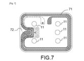
・少なくとも前記集積回路を組み込んだ保護層(21)を堆積させるステップと、を含むことを特徴とする、プロセス。 - アンテナ(71、72)を形成するターンと、前記アンテナの少なくとも一端に配置される少なくとも1つの接触パッド(7p1、7p2)とからなる少なくとも1つの導電性領域(7)を含む基板(6)が使用されることを特徴とする、請求項1に記載のプロセス。
- 前記導電性領域(7)のうちの少なくとも1つは、少なくとも1つの導電材料エリアからなることを特徴とする、請求項1に記載のプロセス。
- 前記導電性領域(7)のうちの少なくとも1つの中央で領域が切り取られ、前記接触部(3)を支える前記片面フィルムの反対側の面に前記集積回路(20)が接合されることを特徴とする、請求項1~3の何れか一項に記載のプロセス。
- 前記集積回路(20)と前記接触領域(3)との間に半田溜りを形成するために前記フィルム内に配置された前記開口部(50)に対応する1つ又は複数の開口部(52、53)が、前記基板と同一水準に作製されることを特徴とする、請求項1~4の何れか一項に記載のプロセス。
- 前記アンテナ又は前記導電材料エリアを形成するためにアルミニウムでできた1つ又は複数の導電性領域を有する基板が使用されることを特徴とする、請求項3に記載のプロセス。
- 前記導電性領域又は前記導電材料エリアのパターンは、エッチング技術、スクリーン印刷による付加的プロセス、又は転写を使用して、生成されることを特徴とする、請求項6に記載のプロセス。
- 接触機能を備える携帯型物体内に実装されることを意図した電子モジュール(2)において、前記電子モジュールは、少なくとも以下の要素、即ち、
・一方の面(4a)および他方の面(4b)を備えた片面フィルム(4)であって、前記片面フィルム(4)は、前記一方の面(4a)上に生成された1つ又は複数の接触部(3)と、前記他方の面(4b)上の誘電体(5)とを支えており、前記誘電体(5)には1つ又は複数の開口部(50)が作製されている、片面フィルム(4)と、
・非接触通信用に意図された1つ又は複数の導電性領域(7)を備える基板(6)であって、前記片面フィルムに固定された基板(6)と、
・前記片面フィルムの前記接触領域、及び、少なくとも、前記導電性領域のうちの少なくとも1つの、1つの端子に接続された集積回路(20)と、
・少なくとも前記集積回路を組み込んだ保護層(21)と、を含むことを特徴とする電子モジュール。 - 前記導電性領域のうちの少なくとも1つは、一端に接続パッド(7p1、7p2)を備えるターン(71、72)の形態を取ることを特徴とする、請求項8に記載のモジュール。
- 前記導電性領域のうちの少なくとも1つは、少なくとも1つの導電材料エリア(75、76)からなることを特徴とする、請求項8に記載のモジュール。
- 前記基板は、集積回路(20)及び前記保護層(21)を収容するのに適した幾何形状を有する、くりぬかれた中央領域を含むことを特徴とする、請求項8~10の何れか一項に記載のモジュール。
- 前記基板は、前記集積回路を前記接触領域に接続するために、前記片面フィルムの前記開口部に対応した1つ又は複数の穿孔を含むことを特徴とする、請求項8~11の何れか一項に記載のモジュール。
- 前記誘電体及び/又は前記基板は、エポキシガラス、ポリエチレンナフタレートPEN、ポリエチレンテレフタレートPET、又はポリ塩化ビニルPVCから選択されることを特徴とする、請求項8~12の何れか一項に記載のモジュール。
Applications Claiming Priority (3)
| Application Number | Priority Date | Filing Date | Title |
|---|---|---|---|
| FR1860297A FR3088515B1 (fr) | 2018-11-08 | 2018-11-08 | Module electronique pour carte a puce |
| FR1860297 | 2018-11-08 | ||
| PCT/EP2019/077275 WO2020094320A1 (fr) | 2018-11-08 | 2019-10-09 | Module electronique pour carte a puce |
Publications (2)
| Publication Number | Publication Date |
|---|---|
| JP2022507119A JP2022507119A (ja) | 2022-01-18 |
| JP7474251B2 true JP7474251B2 (ja) | 2024-04-24 |
Family
ID=66286386
Family Applications (1)
| Application Number | Title | Priority Date | Filing Date |
|---|---|---|---|
| JP2021525330A Active JP7474251B2 (ja) | 2018-11-08 | 2019-10-09 | チップカード用電子モジュール |
Country Status (10)
| Country | Link |
|---|---|
| US (1) | US12505329B2 (ja) |
| EP (1) | EP3877909B1 (ja) |
| JP (1) | JP7474251B2 (ja) |
| KR (1) | KR20210087944A (ja) |
| CN (1) | CN112930540A (ja) |
| BR (1) | BR112021005517A2 (ja) |
| ES (1) | ES3009672T3 (ja) |
| FR (1) | FR3088515B1 (ja) |
| SG (1) | SG11202103548XA (ja) |
| WO (1) | WO2020094320A1 (ja) |
Families Citing this family (5)
| Publication number | Priority date | Publication date | Assignee | Title |
|---|---|---|---|---|
| KR102914017B1 (ko) * | 2020-09-08 | 2026-01-19 | 엘지이노텍 주식회사 | 스마트 ic 기판, 스마트 ic 모듈 및 이를 포함하는 ic 카드 |
| CN116745775A (zh) * | 2021-02-17 | 2023-09-12 | 富士通先端科技株式会社 | Rfid标签 |
| FR3131411B1 (fr) * | 2021-12-24 | 2024-01-05 | Wisekey Semiconductors | Procédé de fabrication d’un module sans contact ayant une bobine d'antenne à inductance finement ajustable |
| FR3131412B1 (fr) * | 2021-12-24 | 2024-01-05 | Wisekey Semiconductors | Module sans contact ayant une bobine d'antenne configurable |
| FR3150614A1 (fr) * | 2023-06-29 | 2025-01-03 | Paragon Identification | Radio-étiquette UHF et procédé de fabrication associé |
Citations (7)
| Publication number | Priority date | Publication date | Assignee | Title |
|---|---|---|---|---|
| JP2002236897A (ja) | 2001-02-07 | 2002-08-23 | Dainippon Printing Co Ltd | 接触・非接触兼用型icモジュールとその製造方法 |
| JP2002298114A (ja) | 2001-03-29 | 2002-10-11 | Dainippon Printing Co Ltd | Icモジュールとその製造方法 |
| JP2002334312A (ja) | 2001-05-11 | 2002-11-22 | Dainippon Printing Co Ltd | 接触・非接触兼用型icモジュールとその製造方法 |
| JP2006024023A (ja) | 2004-07-08 | 2006-01-26 | Tibc:Kk | 接触式icカード用テープキャリアおよび接触式icカード用接触端子モジュール |
| JP2015219878A (ja) | 2014-05-21 | 2015-12-07 | 凸版印刷株式会社 | 複合icカード及びそれに用いる複合icカード用モジュール |
| US20160098628A1 (en) | 2010-12-07 | 2016-04-07 | Nagravision S.A. | Electronic card having an external connector |
| JP2016212778A (ja) | 2015-05-13 | 2016-12-15 | 凸版印刷株式会社 | デュアルインターフェース通信媒体 |
Family Cites Families (19)
| Publication number | Priority date | Publication date | Assignee | Title |
|---|---|---|---|---|
| US5483100A (en) * | 1992-06-02 | 1996-01-09 | Amkor Electronics, Inc. | Integrated circuit package with via interconnections formed in a substrate |
| FR2769390B1 (fr) * | 1997-10-08 | 2003-02-14 | Gemplus Card Int | Procede de fabrication de cartes a puce aptes a assurer un fonctionnement a contact et sans contact, et de cartes a puce sans contact |
| FR2801707B1 (fr) | 1999-11-29 | 2002-02-15 | A S K | Procede de fabrication d'une carte a puce hybride contact- sans contact avec un support d'antenne en materiau fibreux |
| FR2829857B1 (fr) * | 2001-09-14 | 2004-09-17 | A S K | Carte a puce sans contact ou hybride contact-sans contact a tenue renforcee du module electronique |
| KR20030024132A (ko) * | 2001-09-17 | 2003-03-26 | (주)제이티 | 점착성 기판을 이용한 비접촉 ic 카드 및 그 제조방법 |
| DE10356153B4 (de) | 2003-12-02 | 2010-01-14 | Infineon Technologies Ag | Modul für kontaktlose Chipkarten oder Identifizierungssysteme |
| US8030746B2 (en) * | 2008-02-08 | 2011-10-04 | Infineon Technologies Ag | Integrated circuit package |
| US20130134227A1 (en) * | 2010-06-18 | 2013-05-30 | Linxens Holding | Multi-Layered Flexible Printed Circuit and Method of Manufacture |
| US9622359B2 (en) * | 2011-08-08 | 2017-04-11 | Féinics Amatech Teoranta | RFID transponder chip modules |
| US11551051B2 (en) * | 2013-01-18 | 2023-01-10 | Amatech Group Limiied | Coupling frames for smartcards with various module opening shapes |
| US11386317B2 (en) * | 2013-01-18 | 2022-07-12 | Amatech Group Limited | Transponder chip module with module antenna(s) and coupling frame(s) |
| US11341389B2 (en) * | 2013-01-18 | 2022-05-24 | Amatech Group Limited | Manufacturing metal inlays for dual interface metal cards |
| US11928537B2 (en) * | 2013-01-18 | 2024-03-12 | Amatech Group Limited | Manufacturing metal inlays for dual interface metal cards |
| FR3006551B1 (fr) * | 2013-05-30 | 2016-12-09 | Linxens Holding | Procede de fabrication d'un circuit imprime, circuit imprime obtenu par ce procede et module electronique comportant un tel circuit imprime |
| EP2811428A1 (fr) * | 2013-06-07 | 2014-12-10 | Gemalto SA | Procédé de fabrication d'un dispositif radiofréquence avec maintien de connexion anisotropique |
| US9424507B2 (en) * | 2014-04-01 | 2016-08-23 | Nxp B.V. | Dual interface IC card components and method for manufacturing the dual-interface IC card components |
| DE102014106062B4 (de) * | 2014-04-30 | 2018-11-22 | Infineon Technologies Ag | Chipkartenmodul, Chipkartenkörper, Chipkarte und Chipkartenherstellungsverfahren |
| FR3026529B1 (fr) * | 2014-09-30 | 2017-12-29 | Linxens Holding | Procede de fabrication de carte a puce et carte a puce obtenue par ce procede. |
| DE102016114199B4 (de) * | 2016-08-01 | 2021-07-22 | Infineon Technologies Ag | Chipkartenmodul, chipkarte, chipkartenanordnung, verfahren zum ausbilden eines chipkartenmoduls und verfahren zum ausbilden einer chipkarte |
-
2018
- 2018-11-08 FR FR1860297A patent/FR3088515B1/fr active Active
-
2019
- 2019-10-09 BR BR112021005517-7A patent/BR112021005517A2/pt unknown
- 2019-10-09 ES ES19780270T patent/ES3009672T3/es active Active
- 2019-10-09 CN CN201980071664.8A patent/CN112930540A/zh active Pending
- 2019-10-09 WO PCT/EP2019/077275 patent/WO2020094320A1/fr not_active Ceased
- 2019-10-09 KR KR1020217013471A patent/KR20210087944A/ko not_active Ceased
- 2019-10-09 US US17/292,235 patent/US12505329B2/en active Active
- 2019-10-09 EP EP19780270.5A patent/EP3877909B1/fr active Active
- 2019-10-09 SG SG11202103548XA patent/SG11202103548XA/en unknown
- 2019-10-09 JP JP2021525330A patent/JP7474251B2/ja active Active
Patent Citations (7)
| Publication number | Priority date | Publication date | Assignee | Title |
|---|---|---|---|---|
| JP2002236897A (ja) | 2001-02-07 | 2002-08-23 | Dainippon Printing Co Ltd | 接触・非接触兼用型icモジュールとその製造方法 |
| JP2002298114A (ja) | 2001-03-29 | 2002-10-11 | Dainippon Printing Co Ltd | Icモジュールとその製造方法 |
| JP2002334312A (ja) | 2001-05-11 | 2002-11-22 | Dainippon Printing Co Ltd | 接触・非接触兼用型icモジュールとその製造方法 |
| JP2006024023A (ja) | 2004-07-08 | 2006-01-26 | Tibc:Kk | 接触式icカード用テープキャリアおよび接触式icカード用接触端子モジュール |
| US20160098628A1 (en) | 2010-12-07 | 2016-04-07 | Nagravision S.A. | Electronic card having an external connector |
| JP2015219878A (ja) | 2014-05-21 | 2015-12-07 | 凸版印刷株式会社 | 複合icカード及びそれに用いる複合icカード用モジュール |
| JP2016212778A (ja) | 2015-05-13 | 2016-12-15 | 凸版印刷株式会社 | デュアルインターフェース通信媒体 |
Also Published As
| Publication number | Publication date |
|---|---|
| JP2022507119A (ja) | 2022-01-18 |
| ES3009672T3 (en) | 2025-03-31 |
| FR3088515B1 (fr) | 2022-01-28 |
| EP3877909B1 (fr) | 2024-09-25 |
| BR112021005517A2 (pt) | 2021-06-29 |
| WO2020094320A1 (fr) | 2020-05-14 |
| US20210406636A1 (en) | 2021-12-30 |
| EP3877909A1 (fr) | 2021-09-15 |
| FR3088515A1 (fr) | 2020-05-15 |
| CN112930540A (zh) | 2021-06-08 |
| SG11202103548XA (en) | 2021-05-28 |
| KR20210087944A (ko) | 2021-07-13 |
| US12505329B2 (en) | 2025-12-23 |
Similar Documents
| Publication | Publication Date | Title |
|---|---|---|
| US12505329B2 (en) | Electronic module for chip card | |
| CN106415613B (zh) | 用于芯片卡模块的电路的制造方法及用于芯片卡模块的电路 | |
| CN1312626C (zh) | 电路及其制造方法 | |
| US10198684B2 (en) | Smart card module, smart card, and method for producing a smart card module | |
| CN108885709B (zh) | 制造芯片卡和芯片卡天线支撑件的方法 | |
| WO2007125948A1 (ja) | アンテナ内蔵電子回路モジュールとその製造方法 | |
| CN100359682C (zh) | 电子标签及其制造方法 | |
| US10706346B2 (en) | Method for manufacturing a smart card module and a smart card | |
| JP4945682B2 (ja) | 半導体記憶装置およびその製造方法 | |
| US20110073357A1 (en) | Electronic device and method of manufacturing an electronic device | |
| CN104978595A (zh) | 双接口ic卡组件及用于制造双接口ic卡组件的方法 | |
| JP2001325574A (ja) | Icカード | |
| US20060285301A1 (en) | Method for making a pre-laminated inlet | |
| CN112703510B (zh) | 便携式物体的电子模块的制造方法 | |
| CN112714915B (zh) | 制造卡片模块的方法及所获得的模块 | |
| EP3062266B1 (en) | Ic module, ic card, and ic module substrate | |
| CN107423801A (zh) | 智能卡及其制造方法 | |
| JP2010097459A (ja) | Icカード | |
| FR2914460A1 (fr) | Module electronique mince pour carte a microcircuit. | |
| JP2008269648A (ja) | 接触型非接触型共用icカード | |
| JP2007114991A (ja) | 複合icカードと複合icカード用icモジュール | |
| JP2002183696A (ja) | Icカードのコイル製造方法 | |
| CN1936933A (zh) | 微型记忆卡 |
Legal Events
| Date | Code | Title | Description |
|---|---|---|---|
| A621 | Written request for application examination |
Free format text: JAPANESE INTERMEDIATE CODE: A621 Effective date: 20220707 |
|
| A977 | Report on retrieval |
Free format text: JAPANESE INTERMEDIATE CODE: A971007 Effective date: 20230726 |
|
| A131 | Notification of reasons for refusal |
Free format text: JAPANESE INTERMEDIATE CODE: A131 Effective date: 20230905 |
|
| A601 | Written request for extension of time |
Free format text: JAPANESE INTERMEDIATE CODE: A601 Effective date: 20231129 |
|
| A521 | Request for written amendment filed |
Free format text: JAPANESE INTERMEDIATE CODE: A523 Effective date: 20231222 |
|
| TRDD | Decision of grant or rejection written | ||
| A01 | Written decision to grant a patent or to grant a registration (utility model) |
Free format text: JAPANESE INTERMEDIATE CODE: A01 Effective date: 20240319 |
|
| A61 | First payment of annual fees (during grant procedure) |
Free format text: JAPANESE INTERMEDIATE CODE: A61 Effective date: 20240412 |
|
| R150 | Certificate of patent or registration of utility model |
Ref document number: 7474251 Country of ref document: JP Free format text: JAPANESE INTERMEDIATE CODE: R150 |