JP7519992B2 - 半導体の垂直ショットキーダイオード及びその製造方法 - Google Patents
半導体の垂直ショットキーダイオード及びその製造方法 Download PDFInfo
- Publication number
- JP7519992B2 JP7519992B2 JP2021515558A JP2021515558A JP7519992B2 JP 7519992 B2 JP7519992 B2 JP 7519992B2 JP 2021515558 A JP2021515558 A JP 2021515558A JP 2021515558 A JP2021515558 A JP 2021515558A JP 7519992 B2 JP7519992 B2 JP 7519992B2
- Authority
- JP
- Japan
- Prior art keywords
- substrate
- front side
- doped region
- region
- schottky diode
- Prior art date
- Legal status (The legal status is an assumption and is not a legal conclusion. Google has not performed a legal analysis and makes no representation as to the accuracy of the status listed.)
- Active
Links
- 239000004065 semiconductor Substances 0.000 title claims description 53
- 238000000034 method Methods 0.000 title claims description 25
- 238000004519 manufacturing process Methods 0.000 title claims description 24
- 239000000758 substrate Substances 0.000 claims description 97
- 229910052751 metal Inorganic materials 0.000 claims description 56
- 239000002184 metal Substances 0.000 claims description 56
- 229910052710 silicon Inorganic materials 0.000 claims description 46
- 239000010703 silicon Substances 0.000 claims description 46
- 229910021332 silicide Inorganic materials 0.000 claims description 35
- FVBUAEGBCNSCDD-UHFFFAOYSA-N silicide(4-) Chemical compound [Si-4] FVBUAEGBCNSCDD-UHFFFAOYSA-N 0.000 claims description 27
- 238000002955 isolation Methods 0.000 claims description 25
- 239000000463 material Substances 0.000 claims description 13
- 239000003989 dielectric material Substances 0.000 claims description 7
- 238000005530 etching Methods 0.000 claims description 5
- 238000007667 floating Methods 0.000 claims description 5
- 230000002093 peripheral effect Effects 0.000 claims description 4
- XUIMIQQOPSSXEZ-UHFFFAOYSA-N Silicon Chemical compound [Si] XUIMIQQOPSSXEZ-UHFFFAOYSA-N 0.000 description 35
- 239000000243 solution Substances 0.000 description 20
- 230000008569 process Effects 0.000 description 16
- 229910017052 cobalt Inorganic materials 0.000 description 14
- 239000010941 cobalt Substances 0.000 description 14
- VYPSYNLAJGMNEJ-UHFFFAOYSA-N Silicium dioxide Chemical compound O=[Si]=O VYPSYNLAJGMNEJ-UHFFFAOYSA-N 0.000 description 13
- 229910052814 silicon oxide Inorganic materials 0.000 description 13
- 230000003071 parasitic effect Effects 0.000 description 12
- GUTLYIVDDKVIGB-UHFFFAOYSA-N cobalt atom Chemical compound [Co] GUTLYIVDDKVIGB-UHFFFAOYSA-N 0.000 description 8
- 238000002347 injection Methods 0.000 description 6
- 239000007924 injection Substances 0.000 description 6
- RYGMFSIKBFXOCR-UHFFFAOYSA-N Copper Chemical compound [Cu] RYGMFSIKBFXOCR-UHFFFAOYSA-N 0.000 description 5
- 229910052782 aluminium Inorganic materials 0.000 description 5
- XAGFODPZIPBFFR-UHFFFAOYSA-N aluminium Chemical compound [Al] XAGFODPZIPBFFR-UHFFFAOYSA-N 0.000 description 5
- 230000008901 benefit Effects 0.000 description 5
- 230000015572 biosynthetic process Effects 0.000 description 5
- 229910052802 copper Inorganic materials 0.000 description 5
- 239000010949 copper Substances 0.000 description 5
- 230000015556 catabolic process Effects 0.000 description 4
- 238000002513 implantation Methods 0.000 description 4
- WFKWXMTUELFFGS-UHFFFAOYSA-N tungsten Chemical compound [W] WFKWXMTUELFFGS-UHFFFAOYSA-N 0.000 description 4
- 229910052721 tungsten Inorganic materials 0.000 description 4
- 239000010937 tungsten Substances 0.000 description 4
- 238000000137 annealing Methods 0.000 description 3
- 239000004020 conductor Substances 0.000 description 3
- 230000008878 coupling Effects 0.000 description 3
- 238000010168 coupling process Methods 0.000 description 3
- 238000005859 coupling reaction Methods 0.000 description 3
- 230000005684 electric field Effects 0.000 description 3
- 239000007943 implant Substances 0.000 description 3
- 238000005498 polishing Methods 0.000 description 3
- 229910052581 Si3N4 Inorganic materials 0.000 description 2
- 230000004888 barrier function Effects 0.000 description 2
- 238000000151 deposition Methods 0.000 description 2
- 238000009826 distribution Methods 0.000 description 2
- 238000005516 engineering process Methods 0.000 description 2
- 230000001771 impaired effect Effects 0.000 description 2
- 229910044991 metal oxide Inorganic materials 0.000 description 2
- 150000004706 metal oxides Chemical class 0.000 description 2
- 238000001465 metallisation Methods 0.000 description 2
- 150000002739 metals Chemical class 0.000 description 2
- 238000000926 separation method Methods 0.000 description 2
- HQVNEWCFYHHQES-UHFFFAOYSA-N silicon nitride Chemical compound N12[Si]34N5[Si]62N3[Si]51N64 HQVNEWCFYHHQES-UHFFFAOYSA-N 0.000 description 2
- 239000000126 substance Substances 0.000 description 2
- 239000004642 Polyimide Substances 0.000 description 1
- 230000009471 action Effects 0.000 description 1
- UMIVXZPTRXBADB-UHFFFAOYSA-N benzocyclobutene Chemical compound C1=CC=C2CCC2=C1 UMIVXZPTRXBADB-UHFFFAOYSA-N 0.000 description 1
- 239000000969 carrier Substances 0.000 description 1
- 230000000295 complement effect Effects 0.000 description 1
- 230000008021 deposition Effects 0.000 description 1
- 238000005421 electrostatic potential Methods 0.000 description 1
- 238000005468 ion implantation Methods 0.000 description 1
- 150000002500 ions Chemical class 0.000 description 1
- 238000012986 modification Methods 0.000 description 1
- 230000004048 modification Effects 0.000 description 1
- 229910021420 polycrystalline silicon Inorganic materials 0.000 description 1
- 229920001721 polyimide Polymers 0.000 description 1
- 229920005591 polysilicon Polymers 0.000 description 1
- 238000011084 recovery Methods 0.000 description 1
Images


Classifications
-
- H—ELECTRICITY
- H10—SEMICONDUCTOR DEVICES; ELECTRIC SOLID-STATE DEVICES NOT OTHERWISE PROVIDED FOR
- H10D—INORGANIC ELECTRIC SEMICONDUCTOR DEVICES
- H10D8/00—Diodes
- H10D8/60—Schottky-barrier diodes
-
- H—ELECTRICITY
- H10—SEMICONDUCTOR DEVICES; ELECTRIC SOLID-STATE DEVICES NOT OTHERWISE PROVIDED FOR
- H10D—INORGANIC ELECTRIC SEMICONDUCTOR DEVICES
- H10D62/00—Semiconductor bodies, or regions thereof, of devices having potential barriers
- H10D62/10—Shapes, relative sizes or dispositions of the regions of the semiconductor bodies; Shapes of the semiconductor bodies
- H10D62/102—Constructional design considerations for preventing surface leakage or controlling electric field concentration
- H10D62/103—Constructional design considerations for preventing surface leakage or controlling electric field concentration for increasing or controlling the breakdown voltage of reverse-biased devices
- H10D62/105—Constructional design considerations for preventing surface leakage or controlling electric field concentration for increasing or controlling the breakdown voltage of reverse-biased devices by having particular doping profiles, shapes or arrangements of PN junctions; by having supplementary regions, e.g. junction termination extension [JTE]
- H10D62/106—Constructional design considerations for preventing surface leakage or controlling electric field concentration for increasing or controlling the breakdown voltage of reverse-biased devices by having particular doping profiles, shapes or arrangements of PN junctions; by having supplementary regions, e.g. junction termination extension [JTE] having supplementary regions doped oppositely to or in rectifying contact with regions of the semiconductor bodies, e.g. guard rings with PN or Schottky junctions
-
- H—ELECTRICITY
- H10—SEMICONDUCTOR DEVICES; ELECTRIC SOLID-STATE DEVICES NOT OTHERWISE PROVIDED FOR
- H10D—INORGANIC ELECTRIC SEMICONDUCTOR DEVICES
- H10D64/00—Electrodes of devices having potential barriers
- H10D64/20—Electrodes characterised by their shapes, relative sizes or dispositions
- H10D64/23—Electrodes carrying the current to be rectified, amplified, oscillated or switched, e.g. sources, drains, anodes or cathodes
-
- H—ELECTRICITY
- H10—SEMICONDUCTOR DEVICES; ELECTRIC SOLID-STATE DEVICES NOT OTHERWISE PROVIDED FOR
- H10D—INORGANIC ELECTRIC SEMICONDUCTOR DEVICES
- H10D8/00—Diodes
- H10D8/01—Manufacture or treatment
- H10D8/051—Manufacture or treatment of Schottky diodes
-
- H—ELECTRICITY
- H10—SEMICONDUCTOR DEVICES; ELECTRIC SOLID-STATE DEVICES NOT OTHERWISE PROVIDED FOR
- H10D—INORGANIC ELECTRIC SEMICONDUCTOR DEVICES
- H10D84/00—Integrated devices formed in or on semiconductor substrates that comprise only semiconducting layers, e.g. on Si wafers or on GaAs-on-Si wafers
- H10D84/80—Integrated devices formed in or on semiconductor substrates that comprise only semiconducting layers, e.g. on Si wafers or on GaAs-on-Si wafers characterised by the integration of at least one component covered by groups H10D12/00 or H10D30/00, e.g. integration of IGFETs
- H10D84/811—Combinations of field-effect devices and one or more diodes, capacitors or resistors
Landscapes
- Electrodes Of Semiconductors (AREA)
- Internal Circuitry In Semiconductor Integrated Circuit Devices (AREA)
Description
-寄生バイポーラトランジスタが存在せず(本ショットキーダイオードの電気的特性が、寄生バイポーラトランジスタの動作によって損なわれることはない)、
-基板電流が極めて小さく(完全な誘電体分離による)、
-逆方向バイアスでのエッジ部のリークが低減する(逆方向バイアスでの等電位面分布がほぼ平坦になり、このことが、ショットキー領域のエッジ部の電場を低減する助けとなっていることに起因して)、ということである。
Claims (10)
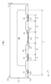
- 集積垂直ショットキーダイオードを備える半導体デバイス(300、400、500、600、700)であって、前記半導体デバイスが、
半導体材料製の基板(101)であって、表側面(101a)及び裏側面(101b’)、並びに前記基板内に形成された集積回路を有する、半導体材料製の基板(101)と、
前記基板(101)の表面部分に形成され、前記表側面(101a)に対向し、かつ第1の導電型を有する低濃度にドープされた領域(102)と、
前記低濃度にドープされた領域(102)における前記基板(101)の前記表側面(101a)に形成され、ショットキー接点を確立している第1の電極(111)と、
前記基板(101)の前記裏側面(101b’)にあり、前記低濃度にドープされた領域(102)と接触しており、かつ第1の導電型を有する高濃度にドープされた領域(140)と、
前記高濃度にドープされた領域(140)における前記基板(101)の前記裏側面(101b’)と電気的に接触して、オーミック接点を確立している第2の電極(160a)と、を備え、
前記基板(101)の前記表側面(101a)にある金属間誘電体層(120)、及び前記金属間誘電体層(120)内で、前記表側面(101a)の上方に配置された少なくとも1つの第1の表側金属相互接続層(121)と、
前記第1の表側金属相互接続層(121)内に画定され、前記表側面(101a)で利用できる第1の電気接点をもたらし、前記金属間誘電体層(120)を貫通して延在している接点(115)を介して、前記第1の電極(111)と電気的に接触している第1の相互接続パッド(121a)と、
前記第1の表側金属相互接続層(121)内に画定され、前記表側面(101a)で利用できる第2の電気接点をもたらす、第2の相互接続パッド(121b)と、
前記基板(101)の前記裏側面(101b’)の上方にあるさらに別の金属間誘電体層(180)、および前記さらに別の金属間誘電体層(180)内に配置された少なくとも1つの第1の相互接続領域(170a、170b)を画定する第1の裏側金属相互接続層と、
誘電体ライナ(161b)及び導電性充填部(161a)を含み、かつ前記低濃度にドープされた領域(102)及び前記高濃度にドープされた領域(140)を横方向に包囲して、電気的分離をもたらしている、シリコン貫通ビア構造(162)と、をさらに備え、
前記シリコン貫通ビア構造(162)が、
前記第2の相互接続パッド(121b)から、前記第2の電極(160a)と電気的接触している前記少なくとも1つの第1の相互接続領域(170a)まで延在し、前記シリコン貫通ビア構造(162)の前記導電性充填部(161a)が、前記第2の電極(160a)と前記第2の相互接続パッド(121b)との間の電気的接触を確立している、
または、前記第1の相互接続パッド(121a)から第2の相互接続領域(170b)まで延在し、前記シリコン貫通ビア構造(162)の前記導電性充填部(161a)が、前記第1の電極(111)と前記第2の相互接続領域(170b)との間の電気的接触を確立しており、これによって前記裏側面(101b’)で利用できる第1の電気接点がもたらされている、
半導体デバイス(300、400、500、600、700)。 - 前記金属間誘電体層(120)の上面(120a)に結合されたキャリアウェーハ(130)をさらに備える、請求項1に記載の半導体デバイス。
- 前記第1の電極(111)が金属シリサイド層から形成されている、請求項1または2に記載の半導体デバイス。
- 第1の導電型とは反対の第2の導電型によって構成され、前記低濃度にドープされた領域(102)の周辺領域における前記基板(101)の前記表側面(101a)に配置されたガードリング(108)をさらに備える、請求項1から3のいずれか一項に記載の半導体デバイス。
- 前記ガードリング(108)が前記第1の電極(111)とオーバーラップし、かつ接触しているか、又は前記第1の電極(111)と接触しておらず、フローティングしている、請求項4に記載の半導体デバイス。
- 前記低濃度にドープされた領域(102)における前記基板(101)の前記表側面(101a)に配置され、幅が同じであり、かつ等距離にある、前記第1の導電型とは反対の第2の導電型を有するドープされた領域(109)のグリッド(188)をさらに備える、請求項1から5のいずれか一項に記載の半導体デバイス。
- 前記基板(101)の前記裏側面(101b’)から、前記低濃度にドープされた領域(102)における前記基板(101)の前記表側面(101a)に形成されたシャロー・トレンチ・アイソレーション(104)まで延在している、誘電体材料から形成されたディープ・トレンチ・アイソレーション領域(106)をさらに備え、前記シャロー・トレンチ・アイソレーション(104)と前記ディープ・トレンチ・アイソレーション領域(106)とが、前記低濃度にドープされた領域(102)及び前記高濃度にドープされた領域(140)を共に横方向に包囲して、誘電体分離をもたらしている、請求項1から6のいずれか一項に記載の半導体デバイス。
- 集積垂直ショットキーダイオードを備える半導体デバイス(300、400、500、600、700)を製造するための方法であって、前記方法が、
半導体材料製の基板(101)であって、上になる表側面(101a)、及び前記表側面(101a)に対向している裏側面(101b)、並びに前記基板内に形成された集積回路を有する、半導体材料製の基板(101)を設け、前記基板(101)の表面部分に、前記表側面(101a)に対向し、かつ第1の導電型を有する、低濃度にドープされた領域(102)を形成するステップと、
ショットキー接点を確立するように、前記低濃度にドープされた領域(102)における前記基板(101)の前記表側面(101a)に第1の電極(111)を形成するステップと、
前記基板(101)の前記表側面(101a)に金属間誘電体層(120)を形成し、かつ前記金属間誘電体層(120)内で、前記表側面(101a)の上方に少なくとも1つの第1の表側金属相互接続層(121)を配置形成するステップと、
前記第1の表側金属相互接続層(121)内に、前記金属間誘電体層(120)を貫通して延在している接点(115)を介して、前記第1の電極(111)と電気的に接触している第1の相互接続パッド(121a)を画定するステップと、
前記基板(101)を反転させ、その結果、前記表側面(101a)に対向している前記基板(101)の前記裏側面(101b)が上になるようにするステップと、
前記基板(101)を前記裏側面(101b)から薄肉化するステップと、
前記基板(101)の前記薄肉化された裏側面(101b’)に、前記低濃度にドープされた領域(102)と接触し、かつ第1の導電型を有する高濃度にドープされた領域(140)を形成するステップと、
前記高濃度にドープされた領域(140)における前記基板(101)の前記薄肉化された裏側面(101b’)と電気的に接触して、オーミック接点を確立するように、第2の電極(160a)を形成するステップと、を含み、
前記基板(101)の前記薄肉化された裏側面(101b’)から前記第1の表側金属相互接続層(121)まで、前記基板(101)を貫通して延在しているシリコン貫通ビア構造(162)を形成するステップであって、前記シリコン貫通ビア構造(162)が、前記低濃度にドープされた領域(102)及び前記高濃度にドープされた領域(140)を横方向に包囲して、電気的分離をもたらしている、ステップと、をさらに含む、
垂直ショットキーダイオードを備える半導体デバイス(300、400、500、600、700)を製造するための方法。 - 前記基板(101)を前記裏側面(101b)から薄肉化する前記ステップが、前記基板(101)の前記表側面(101a)にキャリアウェーハ(130)を結合するステップと、
前記基板(101)において、自身の前記裏側面(101b)を処理するステップと、
前記低濃度にドープされた領域(102)を露出させ、かつ前記裏側面(101b’)を画定するように、前記薄肉化するステップを実行するステップと、をさらに含む、
請求項8に記載の方法。 - 前記第2の電極(160a)を形成する前記ステップが、
前記裏側面(101b’)に誘電体層(150)を形成するステップと、
前記高濃度にドープされた領域(140)の当該領域で、前記誘電体層(150)に接点開口部(152)を貫通エッチングするステップと、
導電性領域で前記接点開口部(152)を充填することにより、前記第2の電極(160a)を構成するステップと、を含む、
請求項9に記載の方法。
Applications Claiming Priority (3)
| Application Number | Priority Date | Filing Date | Title |
|---|---|---|---|
| IT102018000008823 | 2018-09-21 | ||
| IT201800008823 | 2018-09-21 | ||
| PCT/EP2019/075320 WO2020058473A1 (en) | 2018-09-21 | 2019-09-20 | Semiconductor vertical schottky diode and method of manufacturing thereof |
Publications (2)
| Publication Number | Publication Date |
|---|---|
| JP2022500878A JP2022500878A (ja) | 2022-01-04 |
| JP7519992B2 true JP7519992B2 (ja) | 2024-07-22 |
Family
ID=64427137
Family Applications (1)
| Application Number | Title | Priority Date | Filing Date |
|---|---|---|---|
| JP2021515558A Active JP7519992B2 (ja) | 2018-09-21 | 2019-09-20 | 半導体の垂直ショットキーダイオード及びその製造方法 |
Country Status (6)
| Country | Link |
|---|---|
| US (1) | US12119412B2 (ja) |
| EP (1) | EP3853907A1 (ja) |
| JP (1) | JP7519992B2 (ja) |
| KR (1) | KR102787241B1 (ja) |
| CN (1) | CN112740422A (ja) |
| WO (1) | WO2020058473A1 (ja) |
Families Citing this family (3)
| Publication number | Priority date | Publication date | Assignee | Title |
|---|---|---|---|---|
| CN111697057B (zh) * | 2020-06-09 | 2022-07-15 | 杰华特微电子股份有限公司 | 半导体结构及其制造方法 |
| KR102715745B1 (ko) * | 2022-08-08 | 2024-10-11 | 한국기계연구원 | 협대역 쇼트키 다이오드 광센서 및 이를 포함하는 협대역 쇼트키 다이오드 광센서 어레이 |
| CN116093165B (zh) * | 2023-04-10 | 2024-07-23 | 深圳市晶扬电子有限公司 | 一种紧凑的低电容型肖特基二极管 |
Citations (7)
| Publication number | Priority date | Publication date | Assignee | Title |
|---|---|---|---|---|
| JP2007317839A (ja) | 2006-05-25 | 2007-12-06 | Sanyo Electric Co Ltd | 半導体装置およびその製造方法 |
| JP2008166705A (ja) | 2006-12-06 | 2008-07-17 | Denso Corp | 半導体装置およびその製造方法 |
| JP2009064977A (ja) | 2007-09-06 | 2009-03-26 | Renesas Technology Corp | 半導体装置およびその製造方法 |
| JP2012231019A (ja) | 2011-04-26 | 2012-11-22 | Hitachi Ltd | 炭化珪素ダイオード |
| WO2013007705A1 (en) | 2011-07-08 | 2013-01-17 | Stmicroelectronics S.R.L. | Electronic device based on a gallium compound over a silicon substrate, and manufacturing method thereof |
| JP2015207780A (ja) | 2015-06-16 | 2015-11-19 | 富士電機株式会社 | ワイドバンドギャップ半導体装置 |
| JP2017507494A (ja) | 2014-02-28 | 2017-03-16 | エルファウンドリー エッセ エッレ エッレ | 半導体装置の製造方法および半導体製品 |
Family Cites Families (11)
| Publication number | Priority date | Publication date | Assignee | Title |
|---|---|---|---|---|
| US7002187B1 (en) | 2003-06-09 | 2006-02-21 | Micrel, Inc. | Integrated schottky diode using buried power buss structure and method for making same |
| US6825073B1 (en) * | 2003-09-17 | 2004-11-30 | Chip Integration Tech Co., Ltd. | Schottky diode with high field breakdown and low reverse leakage current |
| JP4153932B2 (ja) * | 2004-09-24 | 2008-09-24 | 株式会社東芝 | 半導体装置および半導体装置の製造方法 |
| TW200847448A (en) | 2007-05-30 | 2008-12-01 | Intersil Inc | Junction barrier schottky diode |
| US8013414B2 (en) * | 2009-02-18 | 2011-09-06 | Alpha & Omega Semiconductor, Inc. | Gallium nitride semiconductor device with improved forward conduction |
| US8878329B2 (en) | 2010-09-17 | 2014-11-04 | United Microelectronics Corp. | High voltage device having Schottky diode |
| CN102694033B (zh) | 2011-01-20 | 2015-02-04 | 上海华虹宏力半导体制造有限公司 | 肖特基二极管器件及其制造方法 |
| US9105701B2 (en) * | 2013-06-10 | 2015-08-11 | Micron Technology, Inc. | Semiconductor devices having compact footprints |
| TWI566423B (zh) | 2014-06-19 | 2017-01-11 | 立錡科技股份有限公司 | 接面位障蕭特基二極體 |
| US10157980B1 (en) * | 2017-10-25 | 2018-12-18 | Taiwan Semiconductor Manufacturing Company Ltd. | Semiconductor device having diode devices with different barrier heights and manufacturing method thereof |
| US11521964B2 (en) * | 2018-06-29 | 2022-12-06 | Intel Corporation | Schottky diode structures and integration with III-V transistors |
-
2019
- 2019-09-20 CN CN201980061716.3A patent/CN112740422A/zh active Pending
- 2019-09-20 JP JP2021515558A patent/JP7519992B2/ja active Active
- 2019-09-20 US US17/276,894 patent/US12119412B2/en active Active
- 2019-09-20 EP EP19780173.1A patent/EP3853907A1/en active Pending
- 2019-09-20 WO PCT/EP2019/075320 patent/WO2020058473A1/en not_active Ceased
- 2019-09-20 KR KR1020217011892A patent/KR102787241B1/ko active Active
Patent Citations (7)
| Publication number | Priority date | Publication date | Assignee | Title |
|---|---|---|---|---|
| JP2007317839A (ja) | 2006-05-25 | 2007-12-06 | Sanyo Electric Co Ltd | 半導体装置およびその製造方法 |
| JP2008166705A (ja) | 2006-12-06 | 2008-07-17 | Denso Corp | 半導体装置およびその製造方法 |
| JP2009064977A (ja) | 2007-09-06 | 2009-03-26 | Renesas Technology Corp | 半導体装置およびその製造方法 |
| JP2012231019A (ja) | 2011-04-26 | 2012-11-22 | Hitachi Ltd | 炭化珪素ダイオード |
| WO2013007705A1 (en) | 2011-07-08 | 2013-01-17 | Stmicroelectronics S.R.L. | Electronic device based on a gallium compound over a silicon substrate, and manufacturing method thereof |
| JP2017507494A (ja) | 2014-02-28 | 2017-03-16 | エルファウンドリー エッセ エッレ エッレ | 半導体装置の製造方法および半導体製品 |
| JP2015207780A (ja) | 2015-06-16 | 2015-11-19 | 富士電機株式会社 | ワイドバンドギャップ半導体装置 |
Also Published As
| Publication number | Publication date |
|---|---|
| CN112740422A (zh) | 2021-04-30 |
| KR102787241B1 (ko) | 2025-03-25 |
| WO2020058473A1 (en) | 2020-03-26 |
| KR20210076924A (ko) | 2021-06-24 |
| US20210351304A1 (en) | 2021-11-11 |
| US12119412B2 (en) | 2024-10-15 |
| JP2022500878A (ja) | 2022-01-04 |
| EP3853907A1 (en) | 2021-07-28 |
Similar Documents
| Publication | Publication Date | Title |
|---|---|---|
| US10685955B2 (en) | Trench diode and method of forming the same | |
| EP3742487A1 (en) | An integrated circuit with backside power delivery network and backside transistor | |
| US9129982B2 (en) | Semiconductor device and manufacturing method | |
| US8575695B2 (en) | Lateral super junction device with high substrate-drain breakdown and built-in avalanche clamp diode | |
| US11276688B2 (en) | Monolithic multi-channel diode array | |
| US9911822B2 (en) | Method for manufacturing vertically integrated semiconductor device | |
| US12471301B2 (en) | Integrated circuit and bipolar transistor | |
| TW201705478A (zh) | 具有薄基體之垂直半導體元件 | |
| US9450050B2 (en) | Lateral super junctions with high substrate breakdown and build in avalanche clamp diode | |
| US9406543B2 (en) | Semiconductor power devices and methods of manufacturing the same | |
| US11652167B2 (en) | Semiconductor device having junction termination structure and method of formation | |
| US7220661B1 (en) | Method of manufacturing a Schottky barrier rectifier | |
| US8134219B2 (en) | Schottky diodes | |
| JP7519992B2 (ja) | 半導体の垂直ショットキーダイオード及びその製造方法 | |
| US20090166795A1 (en) | Schottky diode of semiconductor device and method for manufacturing the same | |
| US10529706B2 (en) | Integrated transistor and protection diode and fabrication method | |
| JPS58186965A (ja) | トランジスタ | |
| US20260040613A1 (en) | Gate trench power semiconductor devices having deep channel regions and related methods of fabricating same | |
| US20260075887A1 (en) | Trenched diode having enhanced forward voltage drop to reverse leakage current tradeoff and method of forming such device | |
| WO2026014345A1 (ja) | 半導体装置 |
Legal Events
| Date | Code | Title | Description |
|---|---|---|---|
| RD01 | Notification of change of attorney |
Free format text: JAPANESE INTERMEDIATE CODE: A7426 Effective date: 20210621 |
|
| A521 | Request for written amendment filed |
Free format text: JAPANESE INTERMEDIATE CODE: A821 Effective date: 20210621 |
|
| RD03 | Notification of appointment of power of attorney |
Free format text: JAPANESE INTERMEDIATE CODE: A7423 Effective date: 20211129 |
|
| RD04 | Notification of resignation of power of attorney |
Free format text: JAPANESE INTERMEDIATE CODE: A7424 Effective date: 20211129 |
|
| A621 | Written request for application examination |
Free format text: JAPANESE INTERMEDIATE CODE: A621 Effective date: 20220808 |
|
| A977 | Report on retrieval |
Free format text: JAPANESE INTERMEDIATE CODE: A971007 Effective date: 20230921 |
|
| A131 | Notification of reasons for refusal |
Free format text: JAPANESE INTERMEDIATE CODE: A131 Effective date: 20230925 |
|
| A601 | Written request for extension of time |
Free format text: JAPANESE INTERMEDIATE CODE: A601 Effective date: 20231213 |
|
| A601 | Written request for extension of time |
Free format text: JAPANESE INTERMEDIATE CODE: A601 Effective date: 20240226 |
|
| A521 | Request for written amendment filed |
Free format text: JAPANESE INTERMEDIATE CODE: A523 Effective date: 20240325 |
|
| TRDD | Decision of grant or rejection written | ||
| A01 | Written decision to grant a patent or to grant a registration (utility model) |
Free format text: JAPANESE INTERMEDIATE CODE: A01 Effective date: 20240610 |
|
| A61 | First payment of annual fees (during grant procedure) |
Free format text: JAPANESE INTERMEDIATE CODE: A61 Effective date: 20240709 |
|
| R150 | Certificate of patent or registration of utility model |
Ref document number: 7519992 Country of ref document: JP Free format text: JAPANESE INTERMEDIATE CODE: R150 |