JP7545672B2 - 共振装置、集合基板、及び共振装置の製造方法 - Google Patents
共振装置、集合基板、及び共振装置の製造方法 Download PDFInfo
- Publication number
- JP7545672B2 JP7545672B2 JP2022545290A JP2022545290A JP7545672B2 JP 7545672 B2 JP7545672 B2 JP 7545672B2 JP 2022545290 A JP2022545290 A JP 2022545290A JP 2022545290 A JP2022545290 A JP 2022545290A JP 7545672 B2 JP7545672 B2 JP 7545672B2
- Authority
- JP
- Japan
- Prior art keywords
- substrate
- resonator
- vibration
- resonators
- view
- Prior art date
- Legal status (The legal status is an assumption and is not a legal conclusion. Google has not performed a legal analysis and makes no representation as to the accuracy of the status listed.)
- Active
Links
Images




Classifications
-
- H—ELECTRICITY
- H03—ELECTRONIC CIRCUITRY
- H03H—IMPEDANCE NETWORKS, e.g. RESONANT CIRCUITS; RESONATORS
- H03H9/00—Networks comprising electromechanical or electro-acoustic elements; Electromechanical resonators
- H03H9/02—Details
- H03H9/05—Holders or supports
- H03H9/0595—Holders or supports the holder support and resonator being formed in one body
-
- H—ELECTRICITY
- H03—ELECTRONIC CIRCUITRY
- H03H—IMPEDANCE NETWORKS, e.g. RESONANT CIRCUITS; RESONATORS
- H03H3/00—Apparatus or processes specially adapted for the manufacture of impedance networks, resonating circuits, resonators
- H03H3/007—Apparatus or processes specially adapted for the manufacture of impedance networks, resonating circuits, resonators for the manufacture of electromechanical resonators or networks
- H03H3/0072—Apparatus or processes specially adapted for the manufacture of impedance networks, resonating circuits, resonators for the manufacture of electromechanical resonators or networks of microelectro-mechanical resonators or networks
-
- H—ELECTRICITY
- H03—ELECTRONIC CIRCUITRY
- H03H—IMPEDANCE NETWORKS, e.g. RESONANT CIRCUITS; RESONATORS
- H03H3/00—Apparatus or processes specially adapted for the manufacture of impedance networks, resonating circuits, resonators
- H03H3/007—Apparatus or processes specially adapted for the manufacture of impedance networks, resonating circuits, resonators for the manufacture of electromechanical resonators or networks
- H03H3/0072—Apparatus or processes specially adapted for the manufacture of impedance networks, resonating circuits, resonators for the manufacture of electromechanical resonators or networks of microelectro-mechanical resonators or networks
- H03H3/0076—Apparatus or processes specially adapted for the manufacture of impedance networks, resonating circuits, resonators for the manufacture of electromechanical resonators or networks of microelectro-mechanical resonators or networks for obtaining desired frequency or temperature coefficients
- H03H3/0077—Apparatus or processes specially adapted for the manufacture of impedance networks, resonating circuits, resonators for the manufacture of electromechanical resonators or networks of microelectro-mechanical resonators or networks for obtaining desired frequency or temperature coefficients by tuning of resonance frequency
-
- H—ELECTRICITY
- H03—ELECTRONIC CIRCUITRY
- H03H—IMPEDANCE NETWORKS, e.g. RESONANT CIRCUITS; RESONATORS
- H03H3/00—Apparatus or processes specially adapted for the manufacture of impedance networks, resonating circuits, resonators
- H03H3/007—Apparatus or processes specially adapted for the manufacture of impedance networks, resonating circuits, resonators for the manufacture of electromechanical resonators or networks
- H03H3/013—Apparatus or processes specially adapted for the manufacture of impedance networks, resonating circuits, resonators for the manufacture of electromechanical resonators or networks for obtaining desired frequency or temperature coefficient
-
- H—ELECTRICITY
- H03—ELECTRONIC CIRCUITRY
- H03H—IMPEDANCE NETWORKS, e.g. RESONANT CIRCUITS; RESONATORS
- H03H9/00—Networks comprising electromechanical or electro-acoustic elements; Electromechanical resonators
- H03H9/02—Details
- H03H9/02244—Details of microelectro-mechanical resonators
- H03H9/02433—Means for compensation or elimination of undesired effects
-
- H—ELECTRICITY
- H03—ELECTRONIC CIRCUITRY
- H03H—IMPEDANCE NETWORKS, e.g. RESONANT CIRCUITS; RESONATORS
- H03H9/00—Networks comprising electromechanical or electro-acoustic elements; Electromechanical resonators
- H03H9/02—Details
- H03H9/05—Holders or supports
- H03H9/10—Mounting in enclosures
- H03H9/1057—Mounting in enclosures for microelectro-mechanical devices
-
- H—ELECTRICITY
- H03—ELECTRONIC CIRCUITRY
- H03H—IMPEDANCE NETWORKS, e.g. RESONANT CIRCUITS; RESONATORS
- H03H9/00—Networks comprising electromechanical or electro-acoustic elements; Electromechanical resonators
- H03H9/24—Constructional features of resonators of material which is not piezoelectric, electrostrictive, or magnetostrictive
- H03H9/2405—Constructional features of resonators of material which is not piezoelectric, electrostrictive, or magnetostrictive of microelectro-mechanical resonators
- H03H9/2468—Tuning fork resonators
- H03H9/2478—Single-Ended Tuning Fork resonators
- H03H9/2489—Single-Ended Tuning Fork resonators with more than two fork tines
-
- H—ELECTRICITY
- H03—ELECTRONIC CIRCUITRY
- H03H—IMPEDANCE NETWORKS, e.g. RESONANT CIRCUITS; RESONATORS
- H03H9/00—Networks comprising electromechanical or electro-acoustic elements; Electromechanical resonators
- H03H9/02—Details
- H03H9/02244—Details of microelectro-mechanical resonators
- H03H2009/02488—Vibration modes
-
- H—ELECTRICITY
- H03—ELECTRONIC CIRCUITRY
- H03H—IMPEDANCE NETWORKS, e.g. RESONANT CIRCUITS; RESONATORS
- H03H9/00—Networks comprising electromechanical or electro-acoustic elements; Electromechanical resonators
- H03H9/02—Details
- H03H9/05—Holders or supports
- H03H9/10—Mounting in enclosures
- H03H9/1007—Mounting in enclosures for bulk acoustic wave [BAW] devices
- H03H9/1035—Mounting in enclosures for bulk acoustic wave [BAW] devices the enclosure being defined by two sealing substrates sandwiching the piezoelectric layer of the BAW device
Landscapes
- Physics & Mathematics (AREA)
- Acoustics & Sound (AREA)
- Engineering & Computer Science (AREA)
- Manufacturing & Machinery (AREA)
- Piezo-Electric Or Mechanical Vibrators, Or Delay Or Filter Circuits (AREA)
Description
まず、図1及び図2を参照しつつ、一実施形態に従う共振装置の概略構成について説明する。図1は、一実施形態における共振装置1の外観を概略的に示す斜視図である。図2は、図1に示した共振装置1の構造を概略的に示す分解斜視図である。
次に、図8及び図9を参照しつつ、一実施形態に従う集合基板の概略構成について説明する。図8は、一実施形態における集合基板100の外観を概略的に示す分解斜視図である。図9は、図8に示した領域Aを拡大した部分拡大図である。
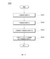
次に、一実施形態に従う共振装置の製造方法について説明する。図10は、一実施形態における共振装置1の製造方法を示すフローチャートである。
図11は、一実施形態の変形例における共振装置1Aの共振子10A及びその周辺の配線を概略的に示す平面図である。図12は、図11に示した連結部材65Aの積層構造を概略的に示す拡大断面図である。
Claims (12)
- 振動部と、該振動部を保持するように構成された保持部と、前記振動部と前記保持部とを接続する支持腕部とを有する共振子を含む第1基板と、
前記共振子を間に挟んで前記第1基板と対向するように配置され、前記振動部と電気的に接続される第1接続部を含む第2基板と、を備え、
前記共振子は、平面視において前記振動部及び前記支持腕部を取り囲むように形成されかつ前記共振子の表面から裏面まで貫通する分離溝をさらに有する、
共振装置。 - 前記共振子の振動空間を封止するように、前記第1基板と前記第2基板とを接合する接合部であって、導電性を有し、前記第1接続部と電気的に接続される接合部と、
前記接合部と電気的に接続され、平面視において前記共振子の外縁まで延在する第2接続部と、をさらに備える、
請求項1に記載の共振装置。 - 前記第2接続部は、前記第1基板の前記第2基板に対向する面と前記第2基板の前記第1基板に対向する面とにおいて、外縁まで延在している、
請求項2に記載の共振装置。 - 前記分離溝は、平面視において前記接合部の外周に配置される、
請求項2又は3に記載の共振装置。 - 前記分離溝は、平面視において前記接合部の内周に配置される、
請求項2又は3に記載の共振装置。 - 前記分離溝は、平面視において前記共振子の外縁と前記振動部との間に配置される、
請求項1から5のいずれか一項に記載の共振装置。 - 前記共振子は、縮退シリコン基板をさらに有する、
請求項1から6のいずれか一項に記載の共振装置。 - 共振装置を製造するための集合基板であって、
それぞれが振動部と、該振動部を保持するように構成された保持部と、前記振動部と前記保持部とを接続する支持腕部とを有する複数の共振子を含む第1基板と、
前記複数の共振子を間に挟んで前記第1基板と対向するように配置され、前記複数の共振子のそれぞれの前記振動部と電気的に接続される複数の第1接続部を含む第2基板と、を備え、
前記複数の共振子は、それぞれ、平面視において前記振動部及び前記支持腕部を取り囲むように形成されかつ前記共振子の表面から裏面まで貫通する分離溝をさらに有する、
集合基板。 - それぞれが前記共振子の振動空間を封止するように、前記第1基板と前記第2基板とを接合する複数の接合部であって、導電性を有し、前記複数の第1接続部のそれぞれと電気的に接続される複数の接合部と、
前記複数の接合部のそれぞれと電気的に接続され、平面視において複数の前記共振装置に分割するための分割ラインを越えて延在する第2接続部と、をさらに備える、
請求項8に記載の集合基板。 - 前記第2接続部は、前記第1基板の前記第2基板に対向する面と前記第2基板の前記第1基板に対向する面とにおいて、前記分割ラインを越えて延在している、
請求項9に記載の集合基板。 - 前記複数の共振子は、縮退シリコン基板をさらに有する、
請求項8から10のいずれか一項に記載の集合基板。 - 共振装置の製造方法であって、
それぞれが振動部と、該振動部を保持するように構成された保持部と、前記振動部と前記保持部とを接続する支持腕部とを有する複数の共振子を含む第1基板と、前記複数の共振子を間に挟んで前記第1基板と対向するように配置され、前記複数の共振子のそれぞれの前記振動部と電気的に接続される複数の第1接続部を含む第2基板と、を準備する工程と、
前記第1基板と前記第2基板とを接合する工程と、
複数の前記共振装置に分割するための分割ラインに沿って前記第1基板及び前記第2基板を分割する工程と、を含み、
前記複数の共振子は、それぞれ、平面視において前記振動部及び前記支持腕部を取り囲むように形成されかつ前記共振子の表面から裏面まで貫通する分離溝をさらに有する、
共振装置の製造方法。
Applications Claiming Priority (3)
| Application Number | Priority Date | Filing Date | Title |
|---|---|---|---|
| JP2020140876 | 2020-08-24 | ||
| JP2020140876 | 2020-08-24 | ||
| PCT/JP2021/010275 WO2022044397A1 (ja) | 2020-08-24 | 2021-03-15 | 共振装置、集合基板、及び共振装置の製造方法 |
Publications (3)
| Publication Number | Publication Date |
|---|---|
| JPWO2022044397A1 JPWO2022044397A1 (ja) | 2022-03-03 |
| JPWO2022044397A5 JPWO2022044397A5 (ja) | 2023-04-26 |
| JP7545672B2 true JP7545672B2 (ja) | 2024-09-05 |
Family
ID=80355054
Family Applications (1)
| Application Number | Title | Priority Date | Filing Date |
|---|---|---|---|
| JP2022545290A Active JP7545672B2 (ja) | 2020-08-24 | 2021-03-15 | 共振装置、集合基板、及び共振装置の製造方法 |
Country Status (4)
| Country | Link |
|---|---|
| US (1) | US20230119602A1 (ja) |
| JP (1) | JP7545672B2 (ja) |
| CN (1) | CN116034542B (ja) |
| WO (1) | WO2022044397A1 (ja) |
Families Citing this family (2)
| Publication number | Priority date | Publication date | Assignee | Title |
|---|---|---|---|---|
| CN116140123B (zh) * | 2022-11-22 | 2026-02-17 | 上海声动微科技有限公司 | 雾化芯片及其制备方法 |
| WO2024161730A1 (ja) * | 2023-02-01 | 2024-08-08 | 株式会社村田製作所 | 共振装置 |
Citations (3)
| Publication number | Priority date | Publication date | Assignee | Title |
|---|---|---|---|---|
| JP2006211310A (ja) | 2005-01-28 | 2006-08-10 | Kyocera Kinseki Corp | 振動子パッケージ |
| JP2013051512A (ja) | 2011-08-30 | 2013-03-14 | Nippon Dempa Kogyo Co Ltd | 水晶振動子 |
| WO2020070942A1 (ja) | 2018-10-05 | 2020-04-09 | 株式会社村田製作所 | 共振子及び共振装置 |
Family Cites Families (3)
| Publication number | Priority date | Publication date | Assignee | Title |
|---|---|---|---|---|
| CN101867080B (zh) * | 2010-05-21 | 2013-02-13 | 中国科学院上海微系统与信息技术研究所 | 一种体硅微机械谐振器及制作方法 |
| CN111095796B (zh) * | 2017-09-28 | 2023-08-18 | 株式会社村田制作所 | 谐振子以及谐振装置 |
| CN110289823B (zh) * | 2019-05-31 | 2021-11-02 | 武汉大学 | 一种微机械谐振器 |
-
2021
- 2021-03-15 WO PCT/JP2021/010275 patent/WO2022044397A1/ja not_active Ceased
- 2021-03-15 JP JP2022545290A patent/JP7545672B2/ja active Active
- 2021-03-15 CN CN202180056420.XA patent/CN116034542B/zh active Active
-
2022
- 2022-12-16 US US18/067,256 patent/US20230119602A1/en active Pending
Patent Citations (3)
| Publication number | Priority date | Publication date | Assignee | Title |
|---|---|---|---|---|
| JP2006211310A (ja) | 2005-01-28 | 2006-08-10 | Kyocera Kinseki Corp | 振動子パッケージ |
| JP2013051512A (ja) | 2011-08-30 | 2013-03-14 | Nippon Dempa Kogyo Co Ltd | 水晶振動子 |
| WO2020070942A1 (ja) | 2018-10-05 | 2020-04-09 | 株式会社村田製作所 | 共振子及び共振装置 |
Also Published As
| Publication number | Publication date |
|---|---|
| JPWO2022044397A1 (ja) | 2022-03-03 |
| CN116034542B (zh) | 2025-10-21 |
| US20230119602A1 (en) | 2023-04-20 |
| CN116034542A (zh) | 2023-04-28 |
| WO2022044397A1 (ja) | 2022-03-03 |
Similar Documents
| Publication | Publication Date | Title |
|---|---|---|
| WO2019155663A1 (ja) | Memsデバイス | |
| WO2018008198A1 (ja) | 共振子及び共振装置 | |
| US11597648B2 (en) | MEMS device manufacturing method and mems device | |
| US12267060B2 (en) | Resonance device | |
| JP7545672B2 (ja) | 共振装置、集合基板、及び共振装置の製造方法 | |
| JP7154487B2 (ja) | パッケージ構造及びその製造方法 | |
| CN112585870B (zh) | 谐振装置 | |
| JP7584019B2 (ja) | 共振装置及びその製造方法 | |
| JP7482402B2 (ja) | 共振子及び共振装置 | |
| CN112703672B (zh) | 谐振子以及谐振装置 | |
| JP7133134B2 (ja) | 共振装置 | |
| JP7708213B2 (ja) | 共振子及び共振装置 | |
| US12531539B2 (en) | Resonance device, collective board, and method of manufacturing resonance device | |
| US20230208392A1 (en) | Resonance device and resonance device manufacturing method | |
| JP7544146B2 (ja) | 共振子及び共振装置 | |
| CN115398802B (zh) | 谐振子以及谐振装置 | |
| JP7591182B2 (ja) | 共振装置及びその製造方法 | |
| WO2022168364A1 (ja) | 共振装置、集合基板、及び共振装置の製造方法 | |
| JP7680716B2 (ja) | 共振装置及び共振装置の製造方法 | |
| WO2023007787A1 (ja) | 共振装置及びその製造方法 | |
| WO2022163020A1 (ja) | 共振装置及びその製造方法 | |
| CN119256490A (zh) | 谐振装置及其制造方法 | |
| CN117730482A (zh) | 谐振子以及谐振装置 |
Legal Events
| Date | Code | Title | Description |
|---|---|---|---|
| A521 | Request for written amendment filed |
Free format text: JAPANESE INTERMEDIATE CODE: A523 Effective date: 20230210 |
|
| A621 | Written request for application examination |
Free format text: JAPANESE INTERMEDIATE CODE: A621 Effective date: 20230210 |
|
| A131 | Notification of reasons for refusal |
Free format text: JAPANESE INTERMEDIATE CODE: A131 Effective date: 20240325 |
|
| A521 | Request for written amendment filed |
Free format text: JAPANESE INTERMEDIATE CODE: A523 Effective date: 20240521 |
|
| TRDD | Decision of grant or rejection written | ||
| A01 | Written decision to grant a patent or to grant a registration (utility model) |
Free format text: JAPANESE INTERMEDIATE CODE: A01 Effective date: 20240726 |
|
| A61 | First payment of annual fees (during grant procedure) |
Free format text: JAPANESE INTERMEDIATE CODE: A61 Effective date: 20240808 |
|
| R150 | Certificate of patent or registration of utility model |
Ref document number: 7545672 Country of ref document: JP Free format text: JAPANESE INTERMEDIATE CODE: R150 |