JP7547537B1 - 保持装置 - Google Patents
保持装置 Download PDFInfo
- Publication number
- JP7547537B1 JP7547537B1 JP2023049750A JP2023049750A JP7547537B1 JP 7547537 B1 JP7547537 B1 JP 7547537B1 JP 2023049750 A JP2023049750 A JP 2023049750A JP 2023049750 A JP2023049750 A JP 2023049750A JP 7547537 B1 JP7547537 B1 JP 7547537B1
- Authority
- JP
- Japan
- Prior art keywords
- flow path
- porous body
- section
- gas
- flow passage
- Prior art date
- Legal status (The legal status is an assumption and is not a legal conclusion. Google has not performed a legal analysis and makes no representation as to the accuracy of the status listed.)
- Active
Links
Images




Classifications
-
- B—PERFORMING OPERATIONS; TRANSPORTING
- B25—HAND TOOLS; PORTABLE POWER-DRIVEN TOOLS; MANIPULATORS
- B25B—TOOLS OR BENCH DEVICES NOT OTHERWISE PROVIDED FOR, FOR FASTENING, CONNECTING, DISENGAGING, OR HOLDING
- B25B11/00—Work holders not covered by any preceding group in the subclass, e.g. magnetic work holders, vacuum work holders
- B25B11/005—Vacuum work holders
-
- H—ELECTRICITY
- H10—SEMICONDUCTOR DEVICES; ELECTRIC SOLID-STATE DEVICES NOT OTHERWISE PROVIDED FOR
- H10P—GENERIC PROCESSES OR APPARATUS FOR THE MANUFACTURE OR TREATMENT OF DEVICES COVERED BY CLASS H10
- H10P72/00—Handling or holding of wafers, substrates or devices during manufacture or treatment thereof
- H10P72/70—Handling or holding of wafers, substrates or devices during manufacture or treatment thereof for supporting or gripping
- H10P72/72—Handling or holding of wafers, substrates or devices during manufacture or treatment thereof for supporting or gripping using electrostatic chucks
- H10P72/722—Details of electrostatic chucks
-
- C—CHEMISTRY; METALLURGY
- C23—COATING METALLIC MATERIAL; COATING MATERIAL WITH METALLIC MATERIAL; CHEMICAL SURFACE TREATMENT; DIFFUSION TREATMENT OF METALLIC MATERIAL; COATING BY VACUUM EVAPORATION, BY SPUTTERING, BY ION IMPLANTATION OR BY CHEMICAL VAPOUR DEPOSITION, IN GENERAL; INHIBITING CORROSION OF METALLIC MATERIAL OR INCRUSTATION IN GENERAL
- C23C—COATING METALLIC MATERIAL; COATING MATERIAL WITH METALLIC MATERIAL; SURFACE TREATMENT OF METALLIC MATERIAL BY DIFFUSION INTO THE SURFACE, BY CHEMICAL CONVERSION OR SUBSTITUTION; COATING BY VACUUM EVAPORATION, BY SPUTTERING, BY ION IMPLANTATION OR BY CHEMICAL VAPOUR DEPOSITION, IN GENERAL
- C23C16/00—Chemical coating by decomposition of gaseous compounds, without leaving reaction products of surface material in the coating, i.e. chemical vapour deposition [CVD] processes
- C23C16/44—Chemical coating by decomposition of gaseous compounds, without leaving reaction products of surface material in the coating, i.e. chemical vapour deposition [CVD] processes characterised by the method of coating
- C23C16/458—Chemical coating by decomposition of gaseous compounds, without leaving reaction products of surface material in the coating, i.e. chemical vapour deposition [CVD] processes characterised by the method of coating characterised by the method used for supporting substrates in the reaction chamber
-
- H—ELECTRICITY
- H10—SEMICONDUCTOR DEVICES; ELECTRIC SOLID-STATE DEVICES NOT OTHERWISE PROVIDED FOR
- H10P—GENERIC PROCESSES OR APPARATUS FOR THE MANUFACTURE OR TREATMENT OF DEVICES COVERED BY CLASS H10
- H10P50/00—Etching of wafers, substrates or parts of devices
- H10P50/20—Dry etching; Plasma etching; Reactive-ion etching
- H10P50/24—Dry etching; Plasma etching; Reactive-ion etching of semiconductor materials
- H10P50/242—Dry etching; Plasma etching; Reactive-ion etching of semiconductor materials of Group IV materials
-
- H—ELECTRICITY
- H10—SEMICONDUCTOR DEVICES; ELECTRIC SOLID-STATE DEVICES NOT OTHERWISE PROVIDED FOR
- H10P—GENERIC PROCESSES OR APPARATUS FOR THE MANUFACTURE OR TREATMENT OF DEVICES COVERED BY CLASS H10
- H10P72/00—Handling or holding of wafers, substrates or devices during manufacture or treatment thereof
- H10P72/70—Handling or holding of wafers, substrates or devices during manufacture or treatment thereof for supporting or gripping
-
- H—ELECTRICITY
- H10—SEMICONDUCTOR DEVICES; ELECTRIC SOLID-STATE DEVICES NOT OTHERWISE PROVIDED FOR
- H10P—GENERIC PROCESSES OR APPARATUS FOR THE MANUFACTURE OR TREATMENT OF DEVICES COVERED BY CLASS H10
- H10P72/00—Handling or holding of wafers, substrates or devices during manufacture or treatment thereof
- H10P72/70—Handling or holding of wafers, substrates or devices during manufacture or treatment thereof for supporting or gripping
- H10P72/76—Handling or holding of wafers, substrates or devices during manufacture or treatment thereof for supporting or gripping using mechanical means, e.g. clamps or pinches
- H10P72/7604—Handling or holding of wafers, substrates or devices during manufacture or treatment thereof for supporting or gripping using mechanical means, e.g. clamps or pinches the wafers being placed on a susceptor, stage or support
- H10P72/7616—Handling or holding of wafers, substrates or devices during manufacture or treatment thereof for supporting or gripping using mechanical means, e.g. clamps or pinches the wafers being placed on a susceptor, stage or support characterised by a coating, a hardness or a material
-
- H—ELECTRICITY
- H10—SEMICONDUCTOR DEVICES; ELECTRIC SOLID-STATE DEVICES NOT OTHERWISE PROVIDED FOR
- H10P—GENERIC PROCESSES OR APPARATUS FOR THE MANUFACTURE OR TREATMENT OF DEVICES COVERED BY CLASS H10
- H10P72/00—Handling or holding of wafers, substrates or devices during manufacture or treatment thereof
- H10P72/70—Handling or holding of wafers, substrates or devices during manufacture or treatment thereof for supporting or gripping
- H10P72/76—Handling or holding of wafers, substrates or devices during manufacture or treatment thereof for supporting or gripping using mechanical means, e.g. clamps or pinches
- H10P72/7604—Handling or holding of wafers, substrates or devices during manufacture or treatment thereof for supporting or gripping using mechanical means, e.g. clamps or pinches the wafers being placed on a susceptor, stage or support
- H10P72/7624—Handling or holding of wafers, substrates or devices during manufacture or treatment thereof for supporting or gripping using mechanical means, e.g. clamps or pinches the wafers being placed on a susceptor, stage or support characterised by the mechanical construction of the susceptor, stage or support
Landscapes
- Chemical & Material Sciences (AREA)
- Engineering & Computer Science (AREA)
- Mechanical Engineering (AREA)
- Metallurgy (AREA)
- Materials Engineering (AREA)
- Chemical Kinetics & Catalysis (AREA)
- General Chemical & Material Sciences (AREA)
- Organic Chemistry (AREA)
- Container, Conveyance, Adherence, Positioning, Of Wafer (AREA)
- Drying Of Semiconductors (AREA)
- Chemical Vapour Deposition (AREA)
- Manipulator (AREA)
- Jigs For Machine Tools (AREA)
- Physics & Mathematics (AREA)
- Plasma & Fusion (AREA)
Abstract

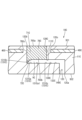
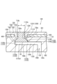
【解決手段】本発明の保持装置100は、対象物Wを保持する第1表面S1、それの反対側に配される第2表面S2を含み、セラミックスを主成分とする板状部材11と、その内部に形成されるガス流路12と、ガス流路12の一部に充填され、セラミックスを主成分とするガス透過性の多孔質体70とを有する保持基板を備える。ガス流路12は、第1表面S1側に開口したガス流出口12bを含み、ガス流出口12bから第2表面S2側に延びた縦流路部120と、縦流路部120と接続し、第1表面S1に対して平行に延びた横流路部130とを有する。多孔質体70は、その第2表面S2側であって横流路部130内に空間Vが形成されるように、縦流路部120に充填される。
【選択図】図3
Description
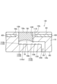
<1> 対象物を保持する第1表面、及び前記第1表面の反対側に配される第2表面を含み、セラミックスを主成分とする板状部材と、前記板状部材の内部に形成されるガス流路と、前記ガス流路の一部に充填され、セラミックスを主成分とするガス透過性の多孔質体とを有する保持基板を備える保持装置であって、前記ガス流路は、前記第1表面側に開口したガス流出口を含み、前記ガス流出口から前記第2表面側に延びた縦流路部と、前記縦流路部と接続し、前記第1表面に対して平行に延びた横流路部とを有し、前記多孔質体は、前記多孔質体の前記第2表面側であって前記横流路部内に空間が形成されるように、前記縦流路部に充填される保持装置。
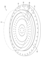
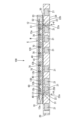
以下、実施形態1に係る保持装置100を、図1~図6を参照しつつ説明する。保持装置100は、対象物(例えば、ウェハW)を、静電引力によって吸着して保持する静電チャックである。静電チャックは、例えば減圧されたチャンバー内でプラズマを用いてエッチングを行うプロセスにおいて、ウェハWを載置するテーブルとして使用される。
次いで、実施形態2に係る保持装置が備える保持基板10Aを、図7を参照しつつ説明する。図7は、実施形態2に係る保持基板10Aの基板側ガス流路12Aの一部を拡大した断面図である。本実施形態の保持基板10Aの基本的な構成は、実施形態1と同じである。そのため、図7では、実施形態1と対応する部分について、実施形態1と同一の符号に更に符号「A」を追加した符号を付し、詳細な説明を省略する。
次いで、実施形態3に係る保持装置が備える保持基板10Bを、図8を参照しつつ説明する。図8は、実施形態3に係る保持基板10Bの基板側ガス流路12Bの一部を拡大した断面図である。本実施形態の保持基板10Bの基本的な構成は、実施形態1と同じである。そのため、図8では、実施形態1と対応する部分について、実施形態1と同一の符号に更に符号「B」を追加した符号を付し、詳細な説明を省略する。
次いで、実施形態4に係る保持装置が備える保持基板10Cを、図9を参照しつつ説明する。図9は、実施形態4に係る保持基板10Cの基板側ガス流路12Cの一部を拡大した断面図である。本実施形態の保持基板10Cの基本的な構成は、実施形態1と同じである。そのため、図9では、実施形態1と対応する部分について、実施形態1と同一の符号に更に符号「C」を追加した符号を付し、詳細な説明を省略する。
次いで、実施形態5に係る保持装置が備える保持基板10Dを、図10を参照しつつ説明する。図10は、実施形態5に係る保持基板10Dの基板側ガス流路12Dの一部を拡大した断面図である。本実施形態の保持基板10Dの基本的な構成は、実施形態1と同じである。そのため、図10では、実施形態1と対応する部分について、実施形態1と同一の符号に更に符号「D」を追加した符号を付し、詳細な説明を省略する。
本発明は上記記述及び図面によって説明した実施形態に限定されるものではなく、例えば次のような実施形態も本発明の技術的範囲に含まれる。
Claims (4)
- 対象物を保持する第1表面、及び前記第1表面の反対側に配される第2表面を含み、セラミックスを主成分とする板状部材と、前記板状部材の内部に形成されるガス流路と、前記ガス流路の一部に充填され、セラミックスを主成分とするガス透過性の多孔質体とを有する保持基板を備える保持装置であって、
前記ガス流路は、前記第1表面側に開口したガス流出口を含み、前記ガス流出口から前記第2表面側に延びた縦流路部と、前記縦流路部と接続し、前記第1表面に対して平行に延びた横流路部とを有し、
前記多孔質体は、前記多孔質体の前記第2表面側であって前記横流路部内に空間が形成されるように、前記縦流路部に充填され、
前記多孔質体は、前記空間に面する前記第2表面側の端面からなり、前記第2表面側に盛り上がった凸状端面を有する保持装置。 - 対象物を保持する第1表面、及び前記第1表面の反対側に配される第2表面を含み、セラミックスを主成分とする板状部材と、前記板状部材の内部に形成されるガス流路と、前記ガス流路の一部に充填され、セラミックスを主成分とするガス透過性の多孔質体とを有する保持基板を備える保持装置であって、
前記ガス流路は、前記第1表面側に開口したガス流出口を含み、前記ガス流出口から前記第2表面側に延びた縦流路部と、前記縦流路部と接続し、前記第1表面に対して平行に延びた横流路部とを有し、
前記多孔質体は、前記多孔質体の前記第2表面側であって前記横流路部内に空間が形成されるように、前記縦流路部に充填され、
前記多孔質体は、前記空間に面する前記第2表面側の端面からなり、前記第1表面側に窪んだ凹状端面を有する保持装置。 - 対象物を保持する第1表面、及び前記第1表面の反対側に配される第2表面を含み、セラミックスを主成分とする板状部材と、前記板状部材の内部に形成されるガス流路と、前記ガス流路の一部に充填され、セラミックスを主成分とするガス透過性の多孔質体とを有する保持基板を備える保持装置であって、
前記ガス流路は、前記第1表面側に開口したガス流出口を含み、前記ガス流出口から前記第2表面側に延びた縦流路部と、前記縦流路部と接続し、前記第1表面に対して平行に延びた横流路部とを有し、
前記多孔質体は、前記多孔質体の前記第2表面側であって前記横流路部内に空間が形成されるように、前記縦流路部に充填され、
前記横流路部は、前記多孔質体と対向する底面を含み、
前記多孔質体は、前記縦流路部に充填される本体部と、前記本体部の前記第2表面側に前記空間が形成されると共に前記底面上で前記本体部が支持されるように、前記本体部から前記底面まで延びた支持部とを有する保持装置。 - 前記横流路部の一端に前記空間を有する請求項1から請求項3の何れか一項に記載の保持装置。
Priority Applications (7)
| Application Number | Priority Date | Filing Date | Title |
|---|---|---|---|
| JP2023049750A JP7547537B1 (ja) | 2023-03-27 | 2023-03-27 | 保持装置 |
| CN202380060744.XA CN120858452A (zh) | 2023-03-27 | 2023-11-07 | 保持装置 |
| PCT/JP2023/040004 WO2024202181A1 (ja) | 2023-03-27 | 2023-11-07 | 保持装置 |
| US19/118,647 US20260040883A1 (en) | 2023-03-27 | 2023-11-07 | Retention device |
| KR1020257004759A KR102954486B1 (ko) | 2023-03-27 | 2023-11-07 | 유지 장치 |
| TW113110707A TW202514900A (zh) | 2023-03-27 | 2024-03-22 | 保持裝置 |
| JP2024146219A JP7669578B2 (ja) | 2023-03-27 | 2024-08-28 | 保持装置 |
Applications Claiming Priority (1)
| Application Number | Priority Date | Filing Date | Title |
|---|---|---|---|
| JP2023049750A JP7547537B1 (ja) | 2023-03-27 | 2023-03-27 | 保持装置 |
Related Child Applications (1)
| Application Number | Title | Priority Date | Filing Date |
|---|---|---|---|
| JP2024146219A Division JP7669578B2 (ja) | 2023-03-27 | 2024-08-28 | 保持装置 |
Publications (2)
| Publication Number | Publication Date |
|---|---|
| JP7547537B1 true JP7547537B1 (ja) | 2024-09-09 |
| JP2024138995A JP2024138995A (ja) | 2024-10-09 |
Family
ID=92673280
Family Applications (2)
| Application Number | Title | Priority Date | Filing Date |
|---|---|---|---|
| JP2023049750A Active JP7547537B1 (ja) | 2023-03-27 | 2023-03-27 | 保持装置 |
| JP2024146219A Active JP7669578B2 (ja) | 2023-03-27 | 2024-08-28 | 保持装置 |
Family Applications After (1)
| Application Number | Title | Priority Date | Filing Date |
|---|---|---|---|
| JP2024146219A Active JP7669578B2 (ja) | 2023-03-27 | 2024-08-28 | 保持装置 |
Country Status (6)
| Country | Link |
|---|---|
| US (1) | US20260040883A1 (ja) |
| JP (2) | JP7547537B1 (ja) |
| KR (1) | KR102954486B1 (ja) |
| CN (1) | CN120858452A (ja) |
| TW (1) | TW202514900A (ja) |
| WO (1) | WO2024202181A1 (ja) |
Citations (8)
| Publication number | Priority date | Publication date | Assignee | Title |
|---|---|---|---|---|
| JP2005268654A (ja) | 2004-03-19 | 2005-09-29 | Ngk Spark Plug Co Ltd | 静電チャック |
| JP2020150071A (ja) | 2019-03-12 | 2020-09-17 | 新光電気工業株式会社 | 基板固定装置 |
| WO2020185395A1 (en) | 2019-03-08 | 2020-09-17 | Applied Materials, Inc. | Electrostatic chuck for high bias radio frequency (rf) power application in a plasma processing chamber |
| JP2021048243A (ja) | 2019-09-18 | 2021-03-25 | 新光電気工業株式会社 | 基板固定装置 |
| JP2021093436A (ja) | 2019-12-10 | 2021-06-17 | 新光電気工業株式会社 | 静電チャック、基板固定装置 |
| JP2023018840A (ja) | 2021-07-28 | 2023-02-09 | 新光電気工業株式会社 | 静電チャック、基板固定装置及び静電チャックの製造方法 |
| JP2023021622A (ja) | 2021-08-02 | 2023-02-14 | 新光電気工業株式会社 | 静電チャック、基板固定装置 |
| WO2023068099A1 (ja) | 2021-10-20 | 2023-04-27 | 日本特殊陶業株式会社 | 保持装置 |
Family Cites Families (5)
| Publication number | Priority date | Publication date | Assignee | Title |
|---|---|---|---|---|
| US6108189A (en) * | 1996-04-26 | 2000-08-22 | Applied Materials, Inc. | Electrostatic chuck having improved gas conduits |
| US6606234B1 (en) | 2000-09-05 | 2003-08-12 | Saint-Gobain Ceramics & Plastics, Inc. | Electrostatic chuck and method for forming an electrostatic chuck having porous regions for fluid flow |
| US6490145B1 (en) * | 2001-07-18 | 2002-12-03 | Applied Materials, Inc. | Substrate support pedestal |
| KR20090097229A (ko) * | 2008-03-11 | 2009-09-16 | 전영재 | 반도체 및 lcd 제조용 정전척 |
| JP6865145B2 (ja) * | 2016-12-16 | 2021-04-28 | 日本特殊陶業株式会社 | 保持装置 |
-
2023
- 2023-03-27 JP JP2023049750A patent/JP7547537B1/ja active Active
- 2023-11-07 US US19/118,647 patent/US20260040883A1/en active Pending
- 2023-11-07 CN CN202380060744.XA patent/CN120858452A/zh active Pending
- 2023-11-07 KR KR1020257004759A patent/KR102954486B1/ko active Active
- 2023-11-07 WO PCT/JP2023/040004 patent/WO2024202181A1/ja not_active Ceased
-
2024
- 2024-03-22 TW TW113110707A patent/TW202514900A/zh unknown
- 2024-08-28 JP JP2024146219A patent/JP7669578B2/ja active Active
Patent Citations (8)
| Publication number | Priority date | Publication date | Assignee | Title |
|---|---|---|---|---|
| JP2005268654A (ja) | 2004-03-19 | 2005-09-29 | Ngk Spark Plug Co Ltd | 静電チャック |
| WO2020185395A1 (en) | 2019-03-08 | 2020-09-17 | Applied Materials, Inc. | Electrostatic chuck for high bias radio frequency (rf) power application in a plasma processing chamber |
| JP2020150071A (ja) | 2019-03-12 | 2020-09-17 | 新光電気工業株式会社 | 基板固定装置 |
| JP2021048243A (ja) | 2019-09-18 | 2021-03-25 | 新光電気工業株式会社 | 基板固定装置 |
| JP2021093436A (ja) | 2019-12-10 | 2021-06-17 | 新光電気工業株式会社 | 静電チャック、基板固定装置 |
| JP2023018840A (ja) | 2021-07-28 | 2023-02-09 | 新光電気工業株式会社 | 静電チャック、基板固定装置及び静電チャックの製造方法 |
| JP2023021622A (ja) | 2021-08-02 | 2023-02-14 | 新光電気工業株式会社 | 静電チャック、基板固定装置 |
| WO2023068099A1 (ja) | 2021-10-20 | 2023-04-27 | 日本特殊陶業株式会社 | 保持装置 |
Also Published As
| Publication number | Publication date |
|---|---|
| CN120858452A (zh) | 2025-10-28 |
| WO2024202181A1 (ja) | 2024-10-03 |
| TW202514900A (zh) | 2025-04-01 |
| KR20250036232A (ko) | 2025-03-13 |
| KR102954486B1 (ko) | 2026-04-17 |
| US20260040883A1 (en) | 2026-02-05 |
| JP2024138995A (ja) | 2024-10-09 |
| JP7669578B2 (ja) | 2025-04-28 |
| JP2024156011A (ja) | 2024-10-31 |
Similar Documents
| Publication | Publication Date | Title |
|---|---|---|
| US12198968B2 (en) | Electrostatic chuck and substrate fixing device | |
| US12567567B2 (en) | Holding device | |
| TWI912585B (zh) | 晶圓載置台 | |
| JP7675814B2 (ja) | シャワープレート | |
| JP7577898B2 (ja) | 保持装置 | |
| CN120513512A (zh) | 晶片载放台 | |
| CN115732386A (zh) | 静电吸盘以及处理装置 | |
| CN120642045A (zh) | 晶片载放台 | |
| JP7551888B1 (ja) | 保持装置 | |
| JP7669578B2 (ja) | 保持装置 | |
| JP7559195B1 (ja) | 保持装置、及び緻密層付き多孔質体 | |
| KR20250068704A (ko) | 유지 장치 | |
| JP7497492B1 (ja) | 保持装置 | |
| JP7507917B1 (ja) | 保持装置 | |
| JP7776669B1 (ja) | ウエハ載置台 | |
| KR102898741B1 (ko) | 정전 척 | |
| JP7627796B1 (ja) | 保持装置 | |
| JP7588686B1 (ja) | 保持装置、保持装置の製造方法、取付体、及び取付体の製造方法 | |
| JP7125262B2 (ja) | シャワーヘッド用ガス分配体 | |
| JP7728464B1 (ja) | 半導体製造装置用部材 | |
| US20250259879A1 (en) | Member for semiconductor manufacturing equipment | |
| JP2022146276A (ja) | セラミックス部材 | |
| JP2012028539A (ja) | セラミックス接合体 |
Legal Events
| Date | Code | Title | Description |
|---|---|---|---|
| A621 | Written request for application examination |
Free format text: JAPANESE INTERMEDIATE CODE: A621 Effective date: 20240226 |
|
| A871 | Explanation of circumstances concerning accelerated examination |
Free format text: JAPANESE INTERMEDIATE CODE: A871 Effective date: 20240226 |
|
| A131 | Notification of reasons for refusal |
Free format text: JAPANESE INTERMEDIATE CODE: A131 Effective date: 20240514 |
|
| A521 | Request for written amendment filed |
Free format text: JAPANESE INTERMEDIATE CODE: A523 Effective date: 20240522 |
|
| TRDD | Decision of grant or rejection written | ||
| A01 | Written decision to grant a patent or to grant a registration (utility model) |
Free format text: JAPANESE INTERMEDIATE CODE: A01 Effective date: 20240801 |
|
| A61 | First payment of annual fees (during grant procedure) |
Free format text: JAPANESE INTERMEDIATE CODE: A61 Effective date: 20240828 |
|
| R150 | Certificate of patent or registration of utility model |
Ref document number: 7547537 Country of ref document: JP Free format text: JAPANESE INTERMEDIATE CODE: R150 |