JP7550730B2 - 半導体装置、半導体モジュール、及び、電力変換装置 - Google Patents
半導体装置、半導体モジュール、及び、電力変換装置 Download PDFInfo
- Publication number
- JP7550730B2 JP7550730B2 JP2021110640A JP2021110640A JP7550730B2 JP 7550730 B2 JP7550730 B2 JP 7550730B2 JP 2021110640 A JP2021110640 A JP 2021110640A JP 2021110640 A JP2021110640 A JP 2021110640A JP 7550730 B2 JP7550730 B2 JP 7550730B2
- Authority
- JP
- Japan
- Prior art keywords
- parallel connection
- connection body
- diode
- parallel
- switching element
- Prior art date
- Legal status (The legal status is an assumption and is not a legal conclusion. Google has not performed a legal analysis and makes no representation as to the accuracy of the status listed.)
- Active
Links
Images

Classifications
-
- H—ELECTRICITY
- H02—GENERATION; CONVERSION OR DISTRIBUTION OF ELECTRIC POWER
- H02M—APPARATUS FOR CONVERSION BETWEEN AC AND AC, BETWEEN AC AND DC, OR BETWEEN DC AND DC, AND FOR USE WITH MAINS OR SIMILAR POWER SUPPLY SYSTEMS; CONVERSION OF DC OR AC INPUT POWER INTO SURGE OUTPUT POWER; CONTROL OR REGULATION THEREOF
- H02M7/00—Conversion of AC power input into DC power output; Conversion of DC power input into AC power output
- H02M7/42—Conversion of DC power input into AC power output without possibility of reversal
- H02M7/44—Conversion of DC power input into AC power output without possibility of reversal by static converters
- H02M7/48—Conversion of DC power input into AC power output without possibility of reversal by static converters using discharge tubes with control electrode or semiconductor devices with control electrode
- H02M7/483—Converters with outputs that each can have more than two voltages levels
- H02M7/487—Neutral point clamped inverters
-
- H—ELECTRICITY
- H02—GENERATION; CONVERSION OR DISTRIBUTION OF ELECTRIC POWER
- H02M—APPARATUS FOR CONVERSION BETWEEN AC AND AC, BETWEEN AC AND DC, OR BETWEEN DC AND DC, AND FOR USE WITH MAINS OR SIMILAR POWER SUPPLY SYSTEMS; CONVERSION OF DC OR AC INPUT POWER INTO SURGE OUTPUT POWER; CONTROL OR REGULATION THEREOF
- H02M1/00—Details of apparatus for conversion
-
- H—ELECTRICITY
- H02—GENERATION; CONVERSION OR DISTRIBUTION OF ELECTRIC POWER
- H02M—APPARATUS FOR CONVERSION BETWEEN AC AND AC, BETWEEN AC AND DC, OR BETWEEN DC AND DC, AND FOR USE WITH MAINS OR SIMILAR POWER SUPPLY SYSTEMS; CONVERSION OF DC OR AC INPUT POWER INTO SURGE OUTPUT POWER; CONTROL OR REGULATION THEREOF
- H02M7/00—Conversion of AC power input into DC power output; Conversion of DC power input into AC power output
- H02M7/003—Constructional details, e.g. physical layout, assembly, wiring or busbar connections
-
- H—ELECTRICITY
- H02—GENERATION; CONVERSION OR DISTRIBUTION OF ELECTRIC POWER
- H02M—APPARATUS FOR CONVERSION BETWEEN AC AND AC, BETWEEN AC AND DC, OR BETWEEN DC AND DC, AND FOR USE WITH MAINS OR SIMILAR POWER SUPPLY SYSTEMS; CONVERSION OF DC OR AC INPUT POWER INTO SURGE OUTPUT POWER; CONTROL OR REGULATION THEREOF
- H02M7/00—Conversion of AC power input into DC power output; Conversion of DC power input into AC power output
- H02M7/42—Conversion of DC power input into AC power output without possibility of reversal
- H02M7/44—Conversion of DC power input into AC power output without possibility of reversal by static converters
- H02M7/48—Conversion of DC power input into AC power output without possibility of reversal by static converters using discharge tubes with control electrode or semiconductor devices with control electrode
- H02M7/483—Converters with outputs that each can have more than two voltages levels
-
- H—ELECTRICITY
- H02—GENERATION; CONVERSION OR DISTRIBUTION OF ELECTRIC POWER
- H02M—APPARATUS FOR CONVERSION BETWEEN AC AND AC, BETWEEN AC AND DC, OR BETWEEN DC AND DC, AND FOR USE WITH MAINS OR SIMILAR POWER SUPPLY SYSTEMS; CONVERSION OF DC OR AC INPUT POWER INTO SURGE OUTPUT POWER; CONTROL OR REGULATION THEREOF
- H02M7/00—Conversion of AC power input into DC power output; Conversion of DC power input into AC power output
- H02M7/42—Conversion of DC power input into AC power output without possibility of reversal
- H02M7/44—Conversion of DC power input into AC power output without possibility of reversal by static converters
- H02M7/48—Conversion of DC power input into AC power output without possibility of reversal by static converters using discharge tubes with control electrode or semiconductor devices with control electrode
- H02M7/53—Conversion of DC power input into AC power output without possibility of reversal by static converters using discharge tubes with control electrode or semiconductor devices with control electrode using devices of a triode or transistor type requiring continuous application of a control signal
- H02M7/537—Conversion of DC power input into AC power output without possibility of reversal by static converters using discharge tubes with control electrode or semiconductor devices with control electrode using devices of a triode or transistor type requiring continuous application of a control signal using semiconductor devices only, e.g. single switched pulse inverters
-
- H—ELECTRICITY
- H10—SEMICONDUCTOR DEVICES; ELECTRIC SOLID-STATE DEVICES NOT OTHERWISE PROVIDED FOR
- H10W—GENERIC PACKAGES, INTERCONNECTIONS, CONNECTORS OR OTHER CONSTRUCTIONAL DETAILS OF DEVICES COVERED BY CLASS H10
- H10W90/00—Package configurations
-
- H—ELECTRICITY
- H10—SEMICONDUCTOR DEVICES; ELECTRIC SOLID-STATE DEVICES NOT OTHERWISE PROVIDED FOR
- H10W—GENERIC PACKAGES, INTERCONNECTIONS, CONNECTORS OR OTHER CONSTRUCTIONAL DETAILS OF DEVICES COVERED BY CLASS H10
- H10W72/00—Interconnections or connectors in packages
- H10W72/071—Connecting or disconnecting
- H10W72/075—Connecting or disconnecting of bond wires
- H10W72/07551—Connecting or disconnecting of bond wires characterised by changes in properties of the bond wires during the connecting
- H10W72/07554—Connecting or disconnecting of bond wires characterised by changes in properties of the bond wires during the connecting changes in dispositions
-
- H—ELECTRICITY
- H10—SEMICONDUCTOR DEVICES; ELECTRIC SOLID-STATE DEVICES NOT OTHERWISE PROVIDED FOR
- H10W—GENERIC PACKAGES, INTERCONNECTIONS, CONNECTORS OR OTHER CONSTRUCTIONAL DETAILS OF DEVICES COVERED BY CLASS H10
- H10W72/00—Interconnections or connectors in packages
- H10W72/50—Bond wires
- H10W72/541—Dispositions of bond wires
- H10W72/5438—Dispositions of bond wires the bond wires having multiple connections on the same bond pad
-
- H—ELECTRICITY
- H10—SEMICONDUCTOR DEVICES; ELECTRIC SOLID-STATE DEVICES NOT OTHERWISE PROVIDED FOR
- H10W—GENERIC PACKAGES, INTERCONNECTIONS, CONNECTORS OR OTHER CONSTRUCTIONAL DETAILS OF DEVICES COVERED BY CLASS H10
- H10W72/00—Interconnections or connectors in packages
- H10W72/50—Bond wires
- H10W72/541—Dispositions of bond wires
- H10W72/5445—Dispositions of bond wires being orthogonal to a side surface of the chip, e.g. parallel arrangements
-
- H—ELECTRICITY
- H10—SEMICONDUCTOR DEVICES; ELECTRIC SOLID-STATE DEVICES NOT OTHERWISE PROVIDED FOR
- H10W—GENERIC PACKAGES, INTERCONNECTIONS, CONNECTORS OR OTHER CONSTRUCTIONAL DETAILS OF DEVICES COVERED BY CLASS H10
- H10W72/00—Interconnections or connectors in packages
- H10W72/50—Bond wires
- H10W72/541—Dispositions of bond wires
- H10W72/547—Dispositions of multiple bond wires
-
- H—ELECTRICITY
- H10—SEMICONDUCTOR DEVICES; ELECTRIC SOLID-STATE DEVICES NOT OTHERWISE PROVIDED FOR
- H10W—GENERIC PACKAGES, INTERCONNECTIONS, CONNECTORS OR OTHER CONSTRUCTIONAL DETAILS OF DEVICES COVERED BY CLASS H10
- H10W72/00—Interconnections or connectors in packages
- H10W72/50—Bond wires
- H10W72/541—Dispositions of bond wires
- H10W72/547—Dispositions of multiple bond wires
- H10W72/5473—Dispositions of multiple bond wires multiple bond wires connected to a common bond pad
-
- H—ELECTRICITY
- H10—SEMICONDUCTOR DEVICES; ELECTRIC SOLID-STATE DEVICES NOT OTHERWISE PROVIDED FOR
- H10W—GENERIC PACKAGES, INTERCONNECTIONS, CONNECTORS OR OTHER CONSTRUCTIONAL DETAILS OF DEVICES COVERED BY CLASS H10
- H10W72/00—Interconnections or connectors in packages
- H10W72/50—Bond wires
- H10W72/541—Dispositions of bond wires
- H10W72/547—Dispositions of multiple bond wires
- H10W72/5475—Dispositions of multiple bond wires multiple bond wires connected to common bond pads at both ends of the wires
-
- H—ELECTRICITY
- H10—SEMICONDUCTOR DEVICES; ELECTRIC SOLID-STATE DEVICES NOT OTHERWISE PROVIDED FOR
- H10W—GENERIC PACKAGES, INTERCONNECTIONS, CONNECTORS OR OTHER CONSTRUCTIONAL DETAILS OF DEVICES COVERED BY CLASS H10
- H10W72/00—Interconnections or connectors in packages
- H10W72/90—Bond pads, in general
- H10W72/921—Structures or relative sizes of bond pads
- H10W72/926—Multiple bond pads having different sizes
Landscapes
- Engineering & Computer Science (AREA)
- Power Engineering (AREA)
- Power Conversion In General (AREA)
- Inverter Devices (AREA)
Description
図1は、本実施の形態1に係る半導体装置の構成を示す回路図である。図1の半導体装置は、3level ANPC(Active Neutral-Point-Clamped)回路であり、第1並列接続体1、第2並列接続体2、第3並列接続体3、第4並列接続体4、第5並列接続体5、及び、第6並列接続体6を備える。
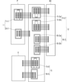
図2は、本実施の形態2に係る半導体装置の構成を示す平面図である。なお、図2では、図が複雑にならないようにゲート配線などの図示を省略している。以下、本実施の形態2のうち、実施の形態1と異なる部分について主に説明する。
本実施の形態3のうち、実施の形態1,2と異なる部分について主に説明する。本実施の形態3では、第2並列接続体2及び第3並列接続体3のそれぞれの、半導体スイッチング素子Tr2,Tr3及びダイオードDi2,Di3の電圧降下のそれぞれは、1.8V以下である。
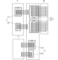
図3は、本実施の形態4に係る半導体装置の構成を示す平面図である。以下、本実施の形態4のうち、実施の形態2と異なる部分について主に説明する。
本実施の形態5のうち、実施の形態1~4と異なる部分について主に説明する。本実施の形態5では、第1並列接続体1、第4並列接続体4、第5並列接続体5、及び、第6並列接続体6の少なくともいずれか1つの、半導体スイッチング素子及びダイオードの少なくともいずれか1つの材料は、ワイドバンドギャップ半導体を含む。ワイドバンドギャップ半導体は、例えば、炭化珪素(SiC)、窒化ガリウム(GaN)、ダイヤモンドなどを含む。
本実施の形態6のうち、実施の形態1~5と異なる部分について主に説明する。本実施の形態6では、第2並列接続体2及び第3並列接続体3の少なくともいずれか1つに含まれるダイオード及び半導体スイッチング素子に関して、ダイオードの予め定められた電流が流れたときのオン電圧が、半導体スイッチング素子の予め定められた電流が流れたときのオン電圧よりも小さい。つまり、第2並列接続体2及び第3並列接続体3の少なくともいずれか1つに含まれるダイオード及び半導体スイッチング素子に関して、ダイオードの電圧降下に対応するVFが、当該ダイオードが接続された半導体スイッチング素子のVcesatよりも小さい。なお、ダイオードのVFを半導体スイッチング素子のVcesatよりも小さくするためには、例えば、ダイオードの有効面積を半導体スイッチング素子の有効面積よりも大きくすればよい。
本実施の形態7のうち、実施の形態1~6と異なる部分について主に説明する。本実施の形態7に係る半導体モジュールは、実施の形態1~6に係る半導体装置と、一の筐体とを備える。一の筐体は、例えば樹脂パッケージであり、第1並列接続体1、第2並列接続体2、及び、第5並列接続体5の組、または、第3並列接続体3、第4並列接続体4、及び、第6並列接続体6の組を覆う。
本実施の形態8のうち、実施の形態1~7と異なる部分について主に説明する。本実施の形態8に係る電力変換装置は、例えばインバータ及びコンバータなどであり、実施の形態1~7に係る半導体装置を備える。このような構成によれば、電力効率が高められた電力変換装置を実現することができる。
Claims (7)
- それぞれが半導体スイッチング素子と前記半導体スイッチング素子に逆並列に接続されたダイオードとを含む、第1並列接続体、第2並列接続体、第3並列接続体、第4並列接続体、第5並列接続体、及び、第6並列接続体を備え、
前記第1並列接続体、前記第2並列接続体、前記第3並列接続体、前記第4並列接続体はこの順に、第1電位の第1端子から、前記第1電位よりも低い第2電位の第2端子までの間に直列に接続され、
前記第2並列接続体と前記第3並列接続体との接続部分は交流端子に接続され、
前記第5並列接続体及び前記第6並列接続体はこの順に、前記第1並列接続体と前記第2並列接続体との接続部分から、前記第3並列接続体と前記第4並列接続体との接続部分までの間に直列に接続され、
前記第5並列接続体と前記第6並列接続体との接続部分は、前記第1電位より小さく前記第2電位より大きい第3電位の第3端子に接続され、
前記第2並列接続体、及び、前記第3並列接続体の電圧降下の少なくともいずれか1つが、前記第1並列接続体、前記第4並列接続体、前記第5並列接続体、及び、前記第6並列接続体の電圧降下の少なくともいずれか1つよりも小さく、
前記第2並列接続体及び前記第3並列接続体の少なくともいずれか1つに含まれる前記半導体スイッチング素子及び前記ダイオードに関して、前記ダイオードの予め定められた電流が流れたときのオン電圧が、前記半導体スイッチング素子の前記予め定められた電流が流れたときのオン電圧よりも小さい、半導体装置。 - 請求項1に記載の半導体装置であって、
前記第2並列接続体、及び、前記第3並列接続体のチップ面積の少なくともいずれか1つが、前記第1並列接続体、前記第4並列接続体、前記第5並列接続体、及び、前記第6並列接続体のチップ面積の少なくともいずれか1つよりも大きい、半導体装置。 - 請求項1または請求項2に記載の半導体装置であって、
前記第2並列接続体及び前記第3並列接続体のそれぞれの、前記半導体スイッチング素子及び前記ダイオードの電圧降下のそれぞれは、1.8V以下である、半導体装置。 - 請求項1から請求項3のうちのいずれか1項に記載の半導体装置であって、
前記第2並列接続体及び前記第3並列接続体の少なくともいずれか1つは、前記半導体スイッチング素子及び前記ダイオードとしてRC-IGBTを含む、半導体装置。 - 請求項1から請求項4のうちのいずれか1項に記載の半導体装置であって、
前記第1並列接続体、前記第4並列接続体、前記第5並列接続体、及び、前記第6並列接続体の少なくともいずれか1つの、前記半導体スイッチング素子及び前記ダイオードの少なくともいずれか1つの材料は、ワイドバンドギャップ半導体を含む、半導体装置。 - 請求項1から請求項5のうちのいずれか1項に記載の半導体装置と、
前記第1並列接続体、前記第2並列接続体、及び、前記第5並列接続体の組、または、前記第3並列接続体、前記第4並列接続体、及び、前記第6並列接続体の組を覆う一の筐体と
を備える、半導体モジュール。 - 請求項1から請求項5のうちのいずれか1項に記載の半導体装置を備える、電力変換装置。
Priority Applications (4)
| Application Number | Priority Date | Filing Date | Title |
|---|---|---|---|
| JP2021110640A JP7550730B2 (ja) | 2021-07-02 | 2021-07-02 | 半導体装置、半導体モジュール、及び、電力変換装置 |
| US17/653,684 US11936305B2 (en) | 2021-07-02 | 2022-03-07 | Semiconductor device, semiconductor module, and power conversion apparatus |
| DE102022111100.8A DE102022111100A1 (de) | 2021-07-02 | 2022-05-05 | Halbleitervorrichtung, Halbleitermodul und Leistungsumwandlungseinrichtung |
| CN202210736114.7A CN115566873A (zh) | 2021-07-02 | 2022-06-27 | 半导体装置、半导体模块及电力转换装置 |
Applications Claiming Priority (1)
| Application Number | Priority Date | Filing Date | Title |
|---|---|---|---|
| JP2021110640A JP7550730B2 (ja) | 2021-07-02 | 2021-07-02 | 半導体装置、半導体モジュール、及び、電力変換装置 |
Publications (2)
| Publication Number | Publication Date |
|---|---|
| JP2023007652A JP2023007652A (ja) | 2023-01-19 |
| JP7550730B2 true JP7550730B2 (ja) | 2024-09-13 |
Family
ID=84492931
Family Applications (1)
| Application Number | Title | Priority Date | Filing Date |
|---|---|---|---|
| JP2021110640A Active JP7550730B2 (ja) | 2021-07-02 | 2021-07-02 | 半導体装置、半導体モジュール、及び、電力変換装置 |
Country Status (4)
| Country | Link |
|---|---|
| US (1) | US11936305B2 (ja) |
| JP (1) | JP7550730B2 (ja) |
| CN (1) | CN115566873A (ja) |
| DE (1) | DE102022111100A1 (ja) |
Citations (5)
| Publication number | Priority date | Publication date | Assignee | Title |
|---|---|---|---|---|
| US20130088901A1 (en) | 2010-03-31 | 2013-04-11 | Ce+T | Multilevel inverter |
| US20140334208A1 (en) | 2013-05-07 | 2014-11-13 | Hamilton Sundstrand Corporation | Synchronous rectification in the three-level inverter-converter topologies |
| JP2017005216A (ja) | 2015-06-16 | 2017-01-05 | 三菱電機株式会社 | 半導体装置 |
| JP2018068083A (ja) | 2016-10-21 | 2018-04-26 | 富士電機株式会社 | 3レベル電力変換装置および整流器 |
| JP2019149882A (ja) | 2018-02-27 | 2019-09-05 | 三菱電機株式会社 | 3レベルiタイプインバータおよび半導体モジュール |
Family Cites Families (3)
| Publication number | Priority date | Publication date | Assignee | Title |
|---|---|---|---|---|
| US20140119088A1 (en) * | 2012-10-29 | 2014-05-01 | Huawei Technologies Co., Ltd. | Three-level inverter and power supply equipment |
| JP6086157B2 (ja) | 2013-10-02 | 2017-03-01 | 富士電機株式会社 | 3レベルインバータ |
| CN107888100B (zh) * | 2016-09-30 | 2019-12-20 | 维谛技术有限公司 | 一种逆变器、控制逆变器的方法及控制装置 |
-
2021
- 2021-07-02 JP JP2021110640A patent/JP7550730B2/ja active Active
-
2022
- 2022-03-07 US US17/653,684 patent/US11936305B2/en active Active
- 2022-05-05 DE DE102022111100.8A patent/DE102022111100A1/de active Pending
- 2022-06-27 CN CN202210736114.7A patent/CN115566873A/zh active Pending
Patent Citations (5)
| Publication number | Priority date | Publication date | Assignee | Title |
|---|---|---|---|---|
| US20130088901A1 (en) | 2010-03-31 | 2013-04-11 | Ce+T | Multilevel inverter |
| US20140334208A1 (en) | 2013-05-07 | 2014-11-13 | Hamilton Sundstrand Corporation | Synchronous rectification in the three-level inverter-converter topologies |
| JP2017005216A (ja) | 2015-06-16 | 2017-01-05 | 三菱電機株式会社 | 半導体装置 |
| JP2018068083A (ja) | 2016-10-21 | 2018-04-26 | 富士電機株式会社 | 3レベル電力変換装置および整流器 |
| JP2019149882A (ja) | 2018-02-27 | 2019-09-05 | 三菱電機株式会社 | 3レベルiタイプインバータおよび半導体モジュール |
Also Published As
| Publication number | Publication date |
|---|---|
| US11936305B2 (en) | 2024-03-19 |
| DE102022111100A1 (de) | 2023-01-05 |
| CN115566873A (zh) | 2023-01-03 |
| JP2023007652A (ja) | 2023-01-19 |
| US20230006571A1 (en) | 2023-01-05 |
Similar Documents
| Publication | Publication Date | Title |
|---|---|---|
| Robles et al. | The role of power device technology in the electric vehicle powertrain | |
| JP6583119B2 (ja) | 電力変換装置 | |
| CN101853847B (zh) | 组合半导体整流器件和使用该组合半导体整流器件的电功率转换器 | |
| US9515061B2 (en) | Semiconductor module and semiconductor device | |
| US6657874B2 (en) | Semiconductor converter circuit and circuit module | |
| CN106921305B (zh) | 三电平功率转换电路 | |
| JPWO2018143429A1 (ja) | 電力用半導体モジュールおよび電力変換装置 | |
| WO2020203001A1 (ja) | 半導体モジュール | |
| JP7337711B2 (ja) | 半導体装置 | |
| JP2018107494A (ja) | 半導体装置及びインバータシステム | |
| JP2019088152A (ja) | 半導体装置及びその駆動方法 | |
| JP6641782B2 (ja) | 電力変換装置 | |
| JP5440438B2 (ja) | パワーモジュール | |
| JP2024008998A (ja) | 電子回路、半導体モジュール及び半導体装置 | |
| Takahashi et al. | Extended power rating of 1200V IGBT module with 7G RCIGBT chip technologies | |
| JP7550730B2 (ja) | 半導体装置、半導体モジュール、及び、電力変換装置 | |
| JP5566354B2 (ja) | 電力用半導体スイッチおよび電力変換装置 | |
| CN117413455A (zh) | 用于功率转换的转换器、三相转换器装置以及用于封装转换器的方法 | |
| Yamano et al. | Expansion of power rating with 7th-Generation" X Series" RC-IGBT Modules for Industrial Applications | |
| US20210351114A1 (en) | Semiconductor package | |
| JP2015201947A (ja) | パワー半導体デバイス | |
| Friedrichs | SiC power devices as enabler for high power density-aspects and prospects | |
| JP6268038B2 (ja) | 半導体装置およびそれを用いた電力変換装置 | |
| JP7178980B2 (ja) | 半導体装置 | |
| Korkh et al. | Dynamic characteristic evaluation of a 600V reverse blocking IGBT device |
Legal Events
| Date | Code | Title | Description |
|---|---|---|---|
| A621 | Written request for application examination |
Free format text: JAPANESE INTERMEDIATE CODE: A621 Effective date: 20230807 |
|
| A977 | Report on retrieval |
Free format text: JAPANESE INTERMEDIATE CODE: A971007 Effective date: 20240327 |
|
| A131 | Notification of reasons for refusal |
Free format text: JAPANESE INTERMEDIATE CODE: A131 Effective date: 20240423 |
|
| A521 | Request for written amendment filed |
Free format text: JAPANESE INTERMEDIATE CODE: A523 Effective date: 20240522 |
|
| TRDD | Decision of grant or rejection written | ||
| A01 | Written decision to grant a patent or to grant a registration (utility model) |
Free format text: JAPANESE INTERMEDIATE CODE: A01 Effective date: 20240806 |
|
| A61 | First payment of annual fees (during grant procedure) |
Free format text: JAPANESE INTERMEDIATE CODE: A61 Effective date: 20240903 |
|
| R150 | Certificate of patent or registration of utility model |
Ref document number: 7550730 Country of ref document: JP Free format text: JAPANESE INTERMEDIATE CODE: R150 |