JP7554523B2 - 発光ダイオードを有する表示画素 - Google Patents
発光ダイオードを有する表示画素 Download PDFInfo
- Publication number
- JP7554523B2 JP7554523B2 JP2023560744A JP2023560744A JP7554523B2 JP 7554523 B2 JP7554523 B2 JP 7554523B2 JP 2023560744 A JP2023560744 A JP 2023560744A JP 2023560744 A JP2023560744 A JP 2023560744A JP 7554523 B2 JP7554523 B2 JP 7554523B2
- Authority
- JP
- Japan
- Prior art keywords
- conductive pad
- signal
- display
- display pixel
- binary signal
- Prior art date
- Legal status (The legal status is an assumption and is not a legal conclusion. Google has not performed a legal analysis and makes no representation as to the accuracy of the status listed.)
- Active
Links
Images



Classifications
-
- G—PHYSICS
- G09—EDUCATION; CRYPTOGRAPHY; DISPLAY; ADVERTISING; SEALS
- G09G—ARRANGEMENTS OR CIRCUITS FOR CONTROL OF INDICATING DEVICES USING STATIC MEANS TO PRESENT VARIABLE INFORMATION
- G09G3/00—Control arrangements or circuits, of interest only in connection with visual indicators other than cathode-ray tubes
- G09G3/20—Control arrangements or circuits, of interest only in connection with visual indicators other than cathode-ray tubes for presentation of an assembly of a number of characters, e.g. a page, by composing the assembly by combination of individual elements arranged in a matrix no fixed position being assigned to or needed to be assigned to the individual characters or partial characters
- G09G3/22—Control arrangements or circuits, of interest only in connection with visual indicators other than cathode-ray tubes for presentation of an assembly of a number of characters, e.g. a page, by composing the assembly by combination of individual elements arranged in a matrix no fixed position being assigned to or needed to be assigned to the individual characters or partial characters using controlled light sources
- G09G3/30—Control arrangements or circuits, of interest only in connection with visual indicators other than cathode-ray tubes for presentation of an assembly of a number of characters, e.g. a page, by composing the assembly by combination of individual elements arranged in a matrix no fixed position being assigned to or needed to be assigned to the individual characters or partial characters using controlled light sources using electroluminescent panels
- G09G3/32—Control arrangements or circuits, of interest only in connection with visual indicators other than cathode-ray tubes for presentation of an assembly of a number of characters, e.g. a page, by composing the assembly by combination of individual elements arranged in a matrix no fixed position being assigned to or needed to be assigned to the individual characters or partial characters using controlled light sources using electroluminescent panels semiconductive, e.g. using light-emitting diodes [LED]
-
- H—ELECTRICITY
- H05—ELECTRIC TECHNIQUES NOT OTHERWISE PROVIDED FOR
- H05B—ELECTRIC HEATING; ELECTRIC LIGHT SOURCES NOT OTHERWISE PROVIDED FOR; CIRCUIT ARRANGEMENTS FOR ELECTRIC LIGHT SOURCES, IN GENERAL
- H05B45/00—Circuit arrangements for operating light-emitting diodes [LED]
- H05B45/30—Driver circuits
- H05B45/32—Pulse-control circuits
- H05B45/325—Pulse-width modulation [PWM]
-
- G—PHYSICS
- G09—EDUCATION; CRYPTOGRAPHY; DISPLAY; ADVERTISING; SEALS
- G09G—ARRANGEMENTS OR CIRCUITS FOR CONTROL OF INDICATING DEVICES USING STATIC MEANS TO PRESENT VARIABLE INFORMATION
- G09G2230/00—Details of flat display driving waveforms
-
- G—PHYSICS
- G09—EDUCATION; CRYPTOGRAPHY; DISPLAY; ADVERTISING; SEALS
- G09G—ARRANGEMENTS OR CIRCUITS FOR CONTROL OF INDICATING DEVICES USING STATIC MEANS TO PRESENT VARIABLE INFORMATION
- G09G2310/00—Command of the display device
- G09G2310/02—Addressing, scanning or driving the display screen or processing steps related thereto
- G09G2310/0264—Details of driving circuits
- G09G2310/027—Details of drivers for data electrodes, the drivers handling digital grey scale data, e.g. use of D/A converters
-
- G—PHYSICS
- G09—EDUCATION; CRYPTOGRAPHY; DISPLAY; ADVERTISING; SEALS
- G09G—ARRANGEMENTS OR CIRCUITS FOR CONTROL OF INDICATING DEVICES USING STATIC MEANS TO PRESENT VARIABLE INFORMATION
- G09G2310/00—Command of the display device
- G09G2310/06—Details of flat display driving waveforms
- G09G2310/065—Waveforms comprising zero voltage phase or pause
-
- G—PHYSICS
- G09—EDUCATION; CRYPTOGRAPHY; DISPLAY; ADVERTISING; SEALS
- G09G—ARRANGEMENTS OR CIRCUITS FOR CONTROL OF INDICATING DEVICES USING STATIC MEANS TO PRESENT VARIABLE INFORMATION
- G09G2310/00—Command of the display device
- G09G2310/08—Details of timing specific for flat panels, other than clock recovery
-
- G—PHYSICS
- G09—EDUCATION; CRYPTOGRAPHY; DISPLAY; ADVERTISING; SEALS
- G09G—ARRANGEMENTS OR CIRCUITS FOR CONTROL OF INDICATING DEVICES USING STATIC MEANS TO PRESENT VARIABLE INFORMATION
- G09G2330/00—Aspects of power supply; Aspects of display protection and defect management
- G09G2330/02—Details of power systems and of start or stop of display operation
- G09G2330/021—Power management, e.g. power saving
-
- G—PHYSICS
- G09—EDUCATION; CRYPTOGRAPHY; DISPLAY; ADVERTISING; SEALS
- G09G—ARRANGEMENTS OR CIRCUITS FOR CONTROL OF INDICATING DEVICES USING STATIC MEANS TO PRESENT VARIABLE INFORMATION
- G09G2330/00—Aspects of power supply; Aspects of display protection and defect management
- G09G2330/02—Details of power systems and of start or stop of display operation
- G09G2330/028—Generation of voltages supplied to electrode drivers in a matrix display other than LCD
Landscapes
- Engineering & Computer Science (AREA)
- Physics & Mathematics (AREA)
- Computer Hardware Design (AREA)
- General Physics & Mathematics (AREA)
- Theoretical Computer Science (AREA)
- Control Of Indicators Other Than Cathode Ray Tubes (AREA)
- Control Of El Displays (AREA)
- Devices For Indicating Variable Information By Combining Individual Elements (AREA)
- Led Device Packages (AREA)
- Led Devices (AREA)
Description
Claims (13)
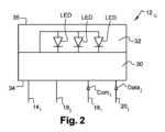
- ディスプレイスクリーンのための表示画素であって、
少なくとも1つの発光ダイオードと、
第1の導電性パッド、第2の導電性パッド、第3の導電性パッド及び第4の導電性パッドと、
前記第1の導電性パッドと前記第2の導電性パッドとの間で受ける第1の電源電圧で少なくとも部分的に電力供給され、前記第3の導電性パッドと前記第2の導電性パッドとの間で受信して前記第1の電源電圧より高い第2の電源電圧と前記第1の電源電圧より低い第3の電圧との間で交互に生じる第1の二値信号が前記第3の電圧の状態を示す各第1のパルス中に前記第4の導電性パッドで受信する第2の二値信号の値に基づきデジタル信号を決定して、前記デジタル信号から前記発光ダイオードを駆動するように構成されている駆動回路と
を備えており、
前記発光ダイオードのアノードが前記第2の導電性パッド及び前記第3の導電性パッドの一方に連結されており、前記発光ダイオードのカソードが前記第2の導電性パッド及び前記第3の導電性パッドの他方に連結されている表示画素。 - 前記駆動回路は、前記デジタル信号からパルス幅変調によって前記発光ダイオードを駆動するように構成されている、請求項1に記載の表示画素。
- 前記第1の導電性パッド、前記第2の導電性パッド、前記第3の導電性パッド及び前記第4の導電性パッドのみを備えている、請求項1又は2に記載の表示画素。
- 前記駆動回路は、前記第1の二値信号が前記第3の電圧の状態を示す第2のパルスで前記発光ダイオードをオン又はオフするように構成されている、請求項1~3のいずれか1つに記載の表示画素。
- 前記駆動回路は、前記第2の二値信号に基づき、前記デジタル信号のビットを示す第3の二値信号、及び前記第3の二値信号を送るタイミングを示すクロック信号を決定するように構成されている、請求項1~4のいずれか1つに記載の表示画素。
- 前記駆動回路は、前記第3の二値信号に基づき各第1のパルスの間に決定される前記デジタル信号を記憶するための回路を有している、請求項5に記載の表示画素。
- 前記第2の二値信号は、同一の継続時間の第3のパルス、及び各第3のパルスの継続時間より長い同一の継続時間の第4のパルスの組合せを含むように構成されており、
前記駆動回路は、前記第3のパルス及び前記第4のパルスと同一のパルスで前記クロック信号を送って、一連の前記第3のパルス及び前記第4のパルスに応じて第1の状態又は第2の状態に等しい前記第3の二値信号を送るように構成されている、請求項5又は6に記載の表示画素。 - 請求項1~7のいずれか1つに記載の表示画素のアレイを備えており、
前記表示画素毎に、前記第1の導電性パッド及び前記第2の導電性パッド間に前記第1の電源電圧を供給して、前記第3の導電性パッド及び前記第2の導電性パッド間に前記第1の二値信号を供給して、前記第4の導電性パッドに前記第2の二値信号を供給するための供給回路を更に備えている、ディスプレイスクリーン。 - 前記供給回路は、前記第1の導電性パッドを実質的に一定の第1の電位に維持して、前記第2の導電性パッドを実質的に一定の第2の電位に維持して、前記第3の導電性パッドを第1の値及び第2の値間で交互に生じる第3の電位で維持するように構成されており、
前記第1の値は前記第1の電位より大きく、前記第2の値は前記第2の電位と等しいか、又は前記第1の値は前記第1の電位と等しく、前記第2の値は前記第2の電位より小さい、請求項8に記載のディスプレイスクリーン。 - 前記供給回路は、0電圧に等しい前記第3の電圧を供給するように構成されている、請求項8又は9に記載のディスプレイスクリーン。
- 前記供給回路は、2つの電位間で交互に生じる前記第2の二値信号を供給するように構成されており、前記2つの電位間の絶対値の差が、前記第1の電源電圧より小さい、請求項8~10のいずれか1つに記載のディスプレイスクリーン。
- 前記供給回路は、画像を表示するために、第1の継続時間を有して前記第3の電圧の状態を示す前記第1のパルスと、前記第1の継続時間より短い第2の継続時間を夫々有する一連の第2のパルスとを有する前記第1の二値信号を供給するように構成されている、請求項8~11のいずれか1つに記載のディスプレイスクリーン。
- 2対の連続する第2のパルス間の継続時間が増加又は減少する、請求項12に記載のディスプレイスクリーン。
Applications Claiming Priority (3)
| Application Number | Priority Date | Filing Date | Title |
|---|---|---|---|
| FR2103309 | 2021-03-31 | ||
| FR2103309A FR3121569B1 (fr) | 2021-03-31 | 2021-03-31 | Pixel d'affichage à diode électroluminescente |
| PCT/EP2022/058460 WO2022207730A1 (fr) | 2021-03-31 | 2022-03-30 | Pixel d'affichage a diode electroluminescente |
Publications (2)
| Publication Number | Publication Date |
|---|---|
| JP2024513859A JP2024513859A (ja) | 2024-03-27 |
| JP7554523B2 true JP7554523B2 (ja) | 2024-09-20 |
Family
ID=76375190
Family Applications (1)
| Application Number | Title | Priority Date | Filing Date |
|---|---|---|---|
| JP2023560744A Active JP7554523B2 (ja) | 2021-03-31 | 2022-03-30 | 発光ダイオードを有する表示画素 |
Country Status (8)
| Country | Link |
|---|---|
| US (1) | US12039922B2 (ja) |
| EP (1) | EP4315308B1 (ja) |
| JP (1) | JP7554523B2 (ja) |
| KR (1) | KR102689431B1 (ja) |
| CN (1) | CN117136400B (ja) |
| FR (1) | FR3121569B1 (ja) |
| TW (1) | TW202244886A (ja) |
| WO (1) | WO2022207730A1 (ja) |
Families Citing this family (3)
| Publication number | Priority date | Publication date | Assignee | Title |
|---|---|---|---|---|
| FR3150040A1 (fr) * | 2023-06-13 | 2024-12-20 | Aledia | Pixel d'affichage comprenant des diodes électroluminescentes pour un écran d'affichage |
| FR3150626A1 (fr) * | 2023-06-29 | 2025-01-03 | Aledia | Écran d'affichage comprenant des pixels d'affichage à diodes électroluminescentes |
| FR3150639A1 (fr) * | 2023-06-29 | 2025-01-03 | Aledia | Ecran d'affichage comportant des pixels d'affichage comprenant des sources luminescentes |
Citations (2)
| Publication number | Priority date | Publication date | Assignee | Title |
|---|---|---|---|---|
| WO2018185433A1 (fr) | 2017-04-05 | 2018-10-11 | Commissariat A L'energie Atomique Et Aux Energies Alternatives | Dispositif d'affichage d'images emissif a led |
| JP2020527757A (ja) | 2017-07-21 | 2020-09-10 | アルディア | 光電子デバイス |
Family Cites Families (14)
| Publication number | Priority date | Publication date | Assignee | Title |
|---|---|---|---|---|
| DE69533982T2 (de) * | 1994-11-21 | 2006-01-05 | Seiko Epson Corp. | Flüssigkristallsteuergerät, flüssigkristallanzeigegerät und flüssigkristallsteuerungsverfahren |
| JP2005099712A (ja) * | 2003-08-28 | 2005-04-14 | Sharp Corp | 表示装置の駆動回路および表示装置 |
| CN1934613A (zh) * | 2004-03-25 | 2007-03-21 | 皇家飞利浦电子股份有限公司 | 显示单元 |
| JP2006054312A (ja) * | 2004-08-11 | 2006-02-23 | Sanyo Electric Co Ltd | 発光素子 |
| US20080303769A1 (en) * | 2007-06-07 | 2008-12-11 | Mitsubishi Electric Corporation | Image display device and drive circuit |
| JP2011023479A (ja) * | 2009-07-14 | 2011-02-03 | Sanyo Electric Co Ltd | 発光ダイオード装置 |
| KR101279661B1 (ko) * | 2010-11-05 | 2013-07-05 | 엘지디스플레이 주식회사 | 입체 영상 표시장치와 그 전원 제어방법 |
| US9640108B2 (en) * | 2015-08-25 | 2017-05-02 | X-Celeprint Limited | Bit-plane pulse width modulated digital display system |
| FR3065117B1 (fr) * | 2017-04-05 | 2019-07-05 | Commissariat A L'energie Atomique Et Aux Energies Alternatives | Dispositif d'affichage d'images emissif a led |
| FR3068819B1 (fr) * | 2017-07-04 | 2019-11-08 | Commissariat A L'energie Atomique Et Aux Energies Alternatives | Dispositif d'affichage a leds |
| FR3070793B1 (fr) * | 2017-09-05 | 2022-07-22 | Commissariat Energie Atomique | Procede de fabrication d'un dispositif d'affichage emissif a led |
| KR101920437B1 (ko) * | 2018-01-09 | 2018-11-20 | (주)실리콘인사이드 | 액티브 매트릭스 구성이 가능한 led 픽셀 패키지 |
| CN109559676A (zh) * | 2018-12-18 | 2019-04-02 | 深圳市奥拓电子股份有限公司 | Led显示驱动电路及led显示屏 |
| CN110191539B (zh) * | 2019-06-10 | 2021-09-07 | 酷矽半导体科技(上海)有限公司 | 驱动电路、驱动芯片及显示系统、显示方法 |
-
2021
- 2021-03-31 FR FR2103309A patent/FR3121569B1/fr active Active
-
2022
- 2022-03-30 US US18/283,785 patent/US12039922B2/en active Active
- 2022-03-30 KR KR1020237035580A patent/KR102689431B1/ko active Active
- 2022-03-30 CN CN202280025625.6A patent/CN117136400B/zh active Active
- 2022-03-30 TW TW111112125A patent/TW202244886A/zh unknown
- 2022-03-30 EP EP22719573.2A patent/EP4315308B1/fr active Active
- 2022-03-30 WO PCT/EP2022/058460 patent/WO2022207730A1/fr not_active Ceased
- 2022-03-30 JP JP2023560744A patent/JP7554523B2/ja active Active
Patent Citations (2)
| Publication number | Priority date | Publication date | Assignee | Title |
|---|---|---|---|---|
| WO2018185433A1 (fr) | 2017-04-05 | 2018-10-11 | Commissariat A L'energie Atomique Et Aux Energies Alternatives | Dispositif d'affichage d'images emissif a led |
| JP2020527757A (ja) | 2017-07-21 | 2020-09-10 | アルディア | 光電子デバイス |
Also Published As
| Publication number | Publication date |
|---|---|
| US12039922B2 (en) | 2024-07-16 |
| CN117136400A (zh) | 2023-11-28 |
| US20240087505A1 (en) | 2024-03-14 |
| KR20230151112A (ko) | 2023-10-31 |
| EP4315308B1 (fr) | 2025-05-07 |
| KR102689431B1 (ko) | 2024-07-26 |
| WO2022207730A1 (fr) | 2022-10-06 |
| EP4315308A1 (fr) | 2024-02-07 |
| FR3121569A1 (fr) | 2022-10-07 |
| FR3121569B1 (fr) | 2023-03-17 |
| JP2024513859A (ja) | 2024-03-27 |
| TW202244886A (zh) | 2022-11-16 |
| CN117136400B (zh) | 2025-07-01 |
Similar Documents
| Publication | Publication Date | Title |
|---|---|---|
| US9082344B2 (en) | Pixel circuit in flat panel display device and method for driving the same | |
| JP7554523B2 (ja) | 発光ダイオードを有する表示画素 | |
| KR100686334B1 (ko) | 표시장치 및 그의 구동방법 | |
| JP7638048B2 (ja) | ディスプレイスクリーンのための発光ダイオードに基づく表示画素 | |
| EP1461797B1 (en) | Electroluminescent display device | |
| JP2010266848A (ja) | El表示装置及びその駆動方法 | |
| US11127354B2 (en) | Display device | |
| KR20210056758A (ko) | 에미션 구동 회로를 포함한 전계발광 표시패널 | |
| JP7531554B2 (ja) | ゲート駆動回路および電界発光表示装置 | |
| CN119889211A (zh) | 显示装置和显示面板 | |
| EP1568004A1 (en) | Colour control for active matrix electroluminescent display | |
| US11996045B2 (en) | Pixel | |
| US20250265960A1 (en) | Display pixel comprising light-emitting sources | |
| US12080227B2 (en) | Pixels and display apparatus comprising same | |
| KR102260511B1 (ko) | 픽셀 및 이를 포함하는 표시장치 | |
| WO2024256298A1 (en) | Display pixel comprising light-emitting diodes for a display screen | |
| JP6142148B2 (ja) | 表示装置 | |
| WO2025003494A1 (en) | Display screen having display pixels comprising light-emitting sources |
Legal Events
| Date | Code | Title | Description |
|---|---|---|---|
| A621 | Written request for application examination |
Free format text: JAPANESE INTERMEDIATE CODE: A621 Effective date: 20231122 |
|
| A871 | Explanation of circumstances concerning accelerated examination |
Free format text: JAPANESE INTERMEDIATE CODE: A871 Effective date: 20231122 |
|
| A131 | Notification of reasons for refusal |
Free format text: JAPANESE INTERMEDIATE CODE: A131 Effective date: 20240409 |
|
| A521 | Request for written amendment filed |
Free format text: JAPANESE INTERMEDIATE CODE: A523 Effective date: 20240708 |
|
| TRDD | Decision of grant or rejection written | ||
| A01 | Written decision to grant a patent or to grant a registration (utility model) |
Free format text: JAPANESE INTERMEDIATE CODE: A01 Effective date: 20240806 |
|
| A61 | First payment of annual fees (during grant procedure) |
Free format text: JAPANESE INTERMEDIATE CODE: A61 Effective date: 20240902 |
|
| R150 | Certificate of patent or registration of utility model |
Ref document number: 7554523 Country of ref document: JP Free format text: JAPANESE INTERMEDIATE CODE: R150 |