JP7559638B2 - Electronics - Google Patents
Electronics Download PDFInfo
- Publication number
- JP7559638B2 JP7559638B2 JP2021045122A JP2021045122A JP7559638B2 JP 7559638 B2 JP7559638 B2 JP 7559638B2 JP 2021045122 A JP2021045122 A JP 2021045122A JP 2021045122 A JP2021045122 A JP 2021045122A JP 7559638 B2 JP7559638 B2 JP 7559638B2
- Authority
- JP
- Japan
- Prior art keywords
- lower arm
- modules
- relay module
- electronic device
- motor
- Prior art date
- Legal status (The legal status is an assumption and is not a legal conclusion. Google has not performed a legal analysis and makes no representation as to the accuracy of the status listed.)
- Active
Links
Images


Classifications
-
- H—ELECTRICITY
- H02—GENERATION; CONVERSION OR DISTRIBUTION OF ELECTRIC POWER
- H02M—APPARATUS FOR CONVERSION BETWEEN AC AND AC, BETWEEN AC AND DC, OR BETWEEN DC AND DC, AND FOR USE WITH MAINS OR SIMILAR POWER SUPPLY SYSTEMS; CONVERSION OF DC OR AC INPUT POWER INTO SURGE OUTPUT POWER; CONTROL OR REGULATION THEREOF
- H02M7/00—Conversion of AC power input into DC power output; Conversion of DC power input into AC power output
- H02M7/003—Constructional details, e.g. physical layout, assembly, wiring or busbar connections
-
- H—ELECTRICITY
- H01—ELECTRIC ELEMENTS
- H01H—ELECTRIC SWITCHES; RELAYS; SELECTORS; EMERGENCY PROTECTIVE DEVICES
- H01H47/00—Circuit arrangements not adapted to a particular application of the relay and designed to obtain desired operating characteristics or to provide energising current
-
- H—ELECTRICITY
- H02—GENERATION; CONVERSION OR DISTRIBUTION OF ELECTRIC POWER
- H02M—APPARATUS FOR CONVERSION BETWEEN AC AND AC, BETWEEN AC AND DC, OR BETWEEN DC AND DC, AND FOR USE WITH MAINS OR SIMILAR POWER SUPPLY SYSTEMS; CONVERSION OF DC OR AC INPUT POWER INTO SURGE OUTPUT POWER; CONTROL OR REGULATION THEREOF
- H02M7/00—Conversion of AC power input into DC power output; Conversion of DC power input into AC power output
- H02M7/42—Conversion of DC power input into AC power output without possibility of reversal
- H02M7/44—Conversion of DC power input into AC power output without possibility of reversal by static converters
- H02M7/48—Conversion of DC power input into AC power output without possibility of reversal by static converters using discharge tubes with control electrode or semiconductor devices with control electrode
- H02M7/53—Conversion of DC power input into AC power output without possibility of reversal by static converters using discharge tubes with control electrode or semiconductor devices with control electrode using devices of a triode or transistor type requiring continuous application of a control signal
- H02M7/537—Conversion of DC power input into AC power output without possibility of reversal by static converters using discharge tubes with control electrode or semiconductor devices with control electrode using devices of a triode or transistor type requiring continuous application of a control signal using semiconductor devices only, e.g. single switched pulse inverters
- H02M7/5387—Conversion of DC power input into AC power output without possibility of reversal by static converters using discharge tubes with control electrode or semiconductor devices with control electrode using devices of a triode or transistor type requiring continuous application of a control signal using semiconductor devices only, e.g. single switched pulse inverters in a bridge configuration
-
- H—ELECTRICITY
- H02—GENERATION; CONVERSION OR DISTRIBUTION OF ELECTRIC POWER
- H02M—APPARATUS FOR CONVERSION BETWEEN AC AND AC, BETWEEN AC AND DC, OR BETWEEN DC AND DC, AND FOR USE WITH MAINS OR SIMILAR POWER SUPPLY SYSTEMS; CONVERSION OF DC OR AC INPUT POWER INTO SURGE OUTPUT POWER; CONTROL OR REGULATION THEREOF
- H02M1/00—Details of apparatus for conversion
- H02M1/0003—Details of control, feedback or regulation circuits
- H02M1/0009—Devices or circuits for detecting current in a converter
-
- H—ELECTRICITY
- H02—GENERATION; CONVERSION OR DISTRIBUTION OF ELECTRIC POWER
- H02M—APPARATUS FOR CONVERSION BETWEEN AC AND AC, BETWEEN AC AND DC, OR BETWEEN DC AND DC, AND FOR USE WITH MAINS OR SIMILAR POWER SUPPLY SYSTEMS; CONVERSION OF DC OR AC INPUT POWER INTO SURGE OUTPUT POWER; CONTROL OR REGULATION THEREOF
- H02M1/00—Details of apparatus for conversion
- H02M1/32—Means for protecting converters other than automatic disconnection
- H02M1/327—Means for protecting converters other than automatic disconnection against abnormal temperatures
-
- H—ELECTRICITY
- H02—GENERATION; CONVERSION OR DISTRIBUTION OF ELECTRIC POWER
- H02M—APPARATUS FOR CONVERSION BETWEEN AC AND AC, BETWEEN AC AND DC, OR BETWEEN DC AND DC, AND FOR USE WITH MAINS OR SIMILAR POWER SUPPLY SYSTEMS; CONVERSION OF DC OR AC INPUT POWER INTO SURGE OUTPUT POWER; CONTROL OR REGULATION THEREOF
- H02M1/00—Details of apparatus for conversion
- H02M1/32—Means for protecting converters other than automatic disconnection
- H02M1/34—Snubber circuits
- H02M1/348—Passive dissipative snubbers
-
- H—ELECTRICITY
- H05—ELECTRIC TECHNIQUES NOT OTHERWISE PROVIDED FOR
- H05K—PRINTED CIRCUITS; CASINGS OR CONSTRUCTIONAL DETAILS OF ELECTRIC APPARATUS; MANUFACTURE OF ASSEMBLAGES OF ELECTRICAL COMPONENTS
- H05K7/00—Constructional details common to different types of electric apparatus
- H05K7/14—Mounting supporting structure in casing or on frame or rack
- H05K7/1438—Back panels or connecting means therefor; Terminals; Coding means to avoid wrong insertion
- H05K7/1457—Power distribution arrangements
Landscapes
- Engineering & Computer Science (AREA)
- Power Engineering (AREA)
- Inverter Devices (AREA)
- Microelectronics & Electronic Packaging (AREA)
- Physics & Mathematics (AREA)
- Thermal Sciences (AREA)
Description
本発明は、電子装置に関する。 The present invention relates to an electronic device.
従来、機電一体型の電動駆動装置が知られている。例えば特許文献1では、電力変換回路を冗長化しており、正極側電源経路と負極側電源経路とを隣接して配設している。
Conventionally, there are known electromechanically integrated electric drive devices. For example, in
特許文献1では、高電位側MOSFET、低電位側MOSFETおよび相リレーMOSFETをそれぞれが個別にパッケージされており、基板上にて駆動回路部の占有面積が大きい。
In
本発明は、上述の課題に鑑みてなされたものであり、その目的は、電流検出素子等の周辺素子を含めた駆動回路を構成する素子の基板占有面積を低減可能な電子装置を提供することにある。 The present invention was made in consideration of the above-mentioned problems, and its purpose is to provide an electronic device that can reduce the substrate area occupied by elements that make up the drive circuit, including peripheral elements such as current detection elements.
本発明の電子装置は、上下アームモジュール(141~143、241~243)と、リレーモジュール(147~149、247~249、351~357)と、周辺部品と、基板(31)と、を備える。上下アームモジュールは、インバータ回路(120、220)を構成する同相の上アーム素子(121~123、221~223)および下アーム素子(124~126、224~226)が1つのモジュールとなっている。リレーモジュールは、上下アームモジュールと出力端子(191~193、291~293)との断接を切替可能なリレー素子(127~129、227~229)が素子毎にモジュールとなっている。周辺部品は、電流検出素子(131~133、231~233)、および、ノイズ除去素子(134~139、234~239)の少なくとも一方を含む。基板は、上下アームモジュール、リレーモジュール、および、周辺部品が実装される。 The electronic device of the present invention comprises upper and lower arm modules (141-143, 241-243), relay modules (147-149, 247-249, 351-357), peripheral components, and a substrate (31). The upper and lower arm modules are formed as one module of upper arm elements (121-123, 221-223) and lower arm elements (124-126, 224-226) of the same phase that constitute an inverter circuit (120, 220). The relay module is formed as a module of relay elements (127-129, 227-229) that can switch between connection and disconnection between the upper and lower arm modules and output terminals (191-193, 291-293), with each element being a module. The peripheral components include at least one of the current detection elements (131-133, 231-233) and the noise elimination elements (134-139, 234-239). The upper and lower arm modules, the relay module, and the peripheral components are mounted on the board.
基板の同一面(391)において、基板中心線から外側に向かい、上下アームモジュール、リレーモジュール、出力端子の順で配列されており、少なくとも一部の周辺部品(131~133、137~139、231~233、237~239)は、上下アームモジュールと出力端子との間の領域にて、リレーモジュールと横並びに配置されている。これにより、インバータ回路および周辺回路の基板占有面積を低減することができる。 On the same surface (391) of the board, the upper and lower arm modules, relay modules, and output terminals are arranged in this order from the board center line outward, and at least some of the peripheral components (131-133, 137-139, 231-233, 237-239) are arranged side-by-side with the relay modules in the area between the upper and lower arm modules and the output terminals. This makes it possible to reduce the board area occupied by the inverter circuit and peripheral circuits.
以下、本発明による電子装置を図面に基づいて説明する。以下、複数の実施形態において、実質的に同一の構成には同一の符号を付して説明を省略する。 The electronic device according to the present invention will be described below with reference to the drawings. In the following, in multiple embodiments, substantially the same configurations are given the same reference numerals and the description will be omitted.
(第1実施形態)
以下、電子装置を図面に基づいて説明する。以下、複数の実施形態において、実質的に同一の構成には同一の符号を付して説明を省略する。第1実施形態による電子制御装置を図1~図9に示す。
First Embodiment
DETAILED DESCRIPTION OF THE PREFERRED EMBODIMENTS The electronic device will be described below with reference to the drawings. In the following, in a number of embodiments, substantially the same components are designated by the same reference numerals, and description thereof will be omitted. An electronic control device according to a first embodiment is shown in FIGS.
図1に示すように、駆動装置1は、モータ80と、ECU10とを備え、車両のステアリング操作を補助するための操舵装置である電動パワーステアリング装置8に適用される。図1は、電動パワーステアリング装置8を備えるステアリングシステム90の全体構成を示すものである。ステアリングシステム90は、操舵部材であるステアリングホイール91、ステアリングシャフト92、ピニオンギア96、ラック軸97、車輪98、および、電動パワーステアリング装置8等を備える。
As shown in FIG. 1, the
ステアリングホイール91は、ステアリングシャフト92と接続される。ステアリングシャフト92には、操舵トルクを検出するトルクセンサ93が設けられる。トルクセンサ93は、内部にて2系統化されており、それぞれの検出値は、対応するコネクタ156、256に入力される。ステアリングシャフト92の先端には、ピニオンギア96が設けられる。ピニオンギア96は、ラック軸97に噛み合っている。ラック軸97の両端には、タイロッド等を介して一対の車輪98が連結される。
The
運転者がステアリングホイール91を回転させると、ステアリングホイール91に接続されたステアリングシャフト92が回転する。ステアリングシャフト92の回転運動は、ピニオンギア96によってラック軸97の直線運動に変換される。一対の車輪98は、ラック軸97の変位量に応じた角度に操舵される。
When the driver turns the
電動パワーステアリング装置8は、駆動装置1、および、モータ80の回転を減速してラック軸97に伝える動力伝達部としての減速ギア89等を備える。本実施形態の電動パワーステアリング装置8は、所謂「ラックアシストタイプ」であるが、モータ80の回転をステアリングシャフト92に伝える所謂「コラムアシストタイプ」等としてもよい。
The electric power steering device 8 includes a
図2~図5に示すように、モータ80は3相ブラシレスモータである。モータ80は、操舵に要するトルクの一部または全部を出力するものであって、図示しないバッテリから電力が供給されることで駆動され、減速ギア89を正逆回転させる。モータ80は、第1モータ巻線180および第2モータ巻線280を有する。
As shown in Figures 2 to 5, the
以下、第1モータ巻線180の通電制御に係る構成の組み合わせを第1系統、第2モータ巻線280の通電制御に係る構成の組み合わせを第2系統とする。第1系統の構成を主に100番台で付番し、第2系統L2の構成を主に200番台で付番し、第1系統と第2系統とで実質的に同様の構成には下2桁が同じとなるように付番し、適宜説明を省略する。また、図中等適宜、第1系統L1に係る構成に添え字の「1」、第2系統L2に係る構成に添え字の「2」を付す。 Hereinafter, the combination of configurations related to the energization control of the first motor winding 180 will be referred to as the first system, and the combination of configurations related to the energization control of the second motor winding 280 will be referred to as the second system. The configurations of the first system L1 will be mainly numbered in the 100s, and the configurations of the second system L2 will be mainly numbered in the 200s. Configurations that are substantially similar in the first and second systems will be numbered so that the last two digits are the same, and explanations will be omitted as appropriate. In addition, as appropriate in the figures, the configurations related to the first system L1 will be given the suffix "1", and the configurations related to the second system L2 will be given the suffix "2".
駆動装置1は、モータ80の軸方向の一方側にECU10が一体的に設けられており、いわゆる「機電一体型」であるが、モータ80とECU10とは別途に設けられていてもよい。ECU10は、モータ80の出力軸とは反対側において、シャフト870の軸Axに対して同軸に配置されている。ここで、「同軸」とは、例えば組み付けや設計に係る誤差やズレは許容されるものとする。なお、本実施形態の駆動装置1における「機電一体」とは、モータ80に対し、例えば概ね直方体形状のECUを単に近接させて設けたものとは異なっている。機電一体型とすることで、搭載スペースに制約のある車両において、ECU10とモータ80とを効率的に配置することができる。以下、モータ80の軸方向を駆動装置1の軸方向とみなし、単に「軸方向」とする。
The
モータ80は、モータケース830、モータフレーム840、ステータ860、および、ロータ865等を有する。ステータ860は、モータケース830に固定されており、モータ巻線180、280が巻回される。ロータ865は、ステータ860の径方向内側に設けられ、ステータ860に対して相対回転可能に設けられる。
The
シャフト870は、ロータ865に嵌入され、ロータ865と一体に回転する。シャフト870は、軸受871、872により、モータケース830およびモータフレーム840に回転可能に支持される。シャフト870のECU10側の端部は、モータフレーム840に形成される軸孔849に挿通され、ECU10側に露出する。シャフト870のECU10側の端部には、マグネット875が設けられる。
The
モータケース830は、底部831および筒部832からなる略有底筒状に形成され、開口側にECU10が設けられる。底部831には、軸受871が設けられる。筒部832には、ステータ860が固定される。
The
モータフレーム840は、フレーム部841、ヒートシンク845、および、コネクタ接続部846等を有し、例えばアルミ等の熱伝導性のよい材料で形成される。フレーム部841は、モータケース830の径方向内側に圧入されており、全体として、モータケース830の筒部832を軸方向に投影した投影領域(以下適宜、「モータシルエット」とする。)内に収まっている。フレーム部841の外周には、フランジ部842が形成され、筒部832の内壁に形成される段差部833と当接する。また、フレーム部841のヒートシンク845の外側には、拡張部材接続部843が形成される。
The
コネクタ接続部846は、モータ巻線180、280が取り出されない側のヒートシンク845の側面の略中央に立設されている。コネクタ接続部846の高さは、ヒートシンク845よりも高い。
The
ECU10は、メイン基板31、サブ基板32、パワー系接続部品101、201、信号系接続部品106、206、コネクタユニット50、および、カバー60等を有する。メイン基板31は、ねじ等の締結部材399にてヒートシンク845に固定される。サブ基板32は、コネクタユニット50に固定される。基板31、32は、軸方向に投影したとき、ヒートシンク845より大きく、ヒートシンク845の外側まで延びて形成されている。
The
メイン基板31のヒートシンク845側の面391には、インバータ回路を構成するスイッチング素子等が実装され、ヒートシンク845に放熱可能に設けられている。メイン基板31のヒートシンク845と反対側の面には、アルミ電解コンデンサ等の部品が実装される。メイン基板31における部品配置は後述する。
Switching elements and the like that constitute the inverter circuit are mounted on the
サブ基板32には、フィルタ回路を構成するチョークコイルおよびコンデンサや、通信ドライバ等の部品が実装される。メイン基板31とサブ基板32とは、パワー系接続部品101、201、および、信号系接続部品106、206で接続される。パワー系接続部品101、201は、素子実装領域の外側にて横並びに配置される。信号系接続部品106、206は、素子実装領域の外側であって、パワー系接続部品101、201とは素子実装領域を挟んで反対側に横並びに配置される。
Components such as choke coils and capacitors that make up the filter circuit, and communication drivers are mounted on the sub-board 32. The
コネクタユニット50は、ベース部51、車両系コネクタ152、252、および、操舵系コネクタ156、256を有する。ベース部51は、平面視略矩形に形成される。ベース部51のモータ80と反対側の面には、外縁に沿って溝部511が形成されている。また、ベース部51には、固定部516が形成される。固定部516には、スルーボルト519が挿通され、モータフレーム840のコネクタ接続部846に螺着される。これにより、コネクタユニット50がモータフレーム840に固定される。モータフレーム840のコネクタ接続部846とコネクタユニット50の固定部516との軸方向における接続位置は、メイン基板31とサブ基板32との間である。
The
コネクタ152、156、252、256は、間口が軸方向外側を向いて形成されている。車両系コネクタ152、252は、車両電源およびグランドと接続されるパワー系コネクタと、CAN(Controller Area Network)等である車両通信網99(図1参照)と接続される通信系コネクタとが一体になった一体型のハイブリッドコネクタである。操舵系コネクタ156、256は、トルクセンサ93と接続される。
The
カバー60は、略有底筒状に形成され、内部に基板31、32およびヒートシンク845等を収容する。カバー60の底部には、略矩形の孔部61が形成される。孔部61には、コネクタ152、156、252、256が挿通される。孔部61は端部611が内側に折り曲げられている。端部611は、接着材等である接着部材が塗布されたコネクタユニット50の溝部511に挿入される。これにより、コネクタユニット50とカバー60との間からの水滴や埃の侵入を防ぐことができる。
The
本実施形態では、車両系コネクタ152、252および操舵系コネクタ156、256の4つの間口を設けており、ベース部51は、モータケース830の筒部832を軸方向に投影した投影領域からはみ出す。換言すると、コネクタユニット50は、モータシルエットに収まっていない。
In this embodiment, four openings are provided for the
拡張部材70は、基部71、環状凸部72、カバー挿入溝73、および、固定部74等を有し、樹脂等にて一体に形成される。拡張部材70は、全体として環状に形成され、モータフレーム840のフレーム部841のECU10側であって、ヒートシンク845の径方向外側に配置される。換言すると、ヒートシンク845は、拡張部材70の内周側にて、ECU10側に突出して形成されている。拡張部材70の外縁の少なくとも一部は、モータシルエットよりも外側に位置している。
The
環状凸部72は、基部71のモータ80側の面に内周面に沿って突出して設けられ、モータケース830の筒部832に挿入される。拡張部材70のモータ80と反対側の面には、カバー挿入溝73が外縁に沿って形成される。カバー60の開口側の端部は、接着材等である接着部材が塗布されたカバー挿入溝73に挿入される。これにより、拡張部材70とカバー60との間からの水滴や埃等の侵入を防ぐことができる。固定部74は、拡張部材70の内周壁から径方向内側に突出して形成される。固定部74には、カラーが挿入され、ねじ79にてフレーム部841に固定される。
The
ここで、駆動装置1の回路構成を図6に示す。本実施形態では、第1系統L1の回路構成と第2系統L2の回路構成とが同じであるので、第1系統L1について説明し、第2系統L2に係る説明を適宜省略する。
The circuit configuration of the
インバータ回路120は、3相インバータであって、高電位側に接続される上アーム素子121~123、および、低電位側に接続される下アーム素子124~126がブリッジ接続されている。インバータ回路120の高電位側は、電源リレー素子111、112を経由してバッテリ等である電源と接続され、低電位側はグランドと接続される。
The
対になるU相の上アーム素子121と下アーム素子124との接続点は、モータリレー素子127およびモータ端子191を経由してU相巻線181の一端と接続される。対になるV相の上アーム素子122と下アーム素子125との接続点は、モータリレー素子128およびモータ端子192を経由してV相巻線182の一端と接続される。対になるW相の上アーム素子123と下アーム素子126との接続点は、モータリレー素子129およびモータ端子193を経由してW相巻線183の一端と接続される。巻線181~183の他端は、結線される。
The connection point between the paired U-phase
下アーム素子124、125、126の低電位側には、モータ巻線180の各相の電流を検出する電流検出素子であるシャント抵抗131、132、133が設けられている。また、上アーム素子121~123および下アーム素子124~126には、ノイズ低減のためのスナバ回路素子134~139が並列に接続されている。スナバ回路素子134~139は、直列に接続されるコンデンサおよび抵抗から構成される。以下、図中等適宜、コンデンサと抵抗とを区別すべく、コンデンサに添え字の「ca」を付し、抵抗に添え字の「r」を付すと共にハッチングを記載した。
インバータ回路120には、電源リレー素子111、112を経由して電力が供給される。本実施形態では、上アーム素子121~123、下アーム素子124~126、モータリレー素子127~129および電源リレー素子111、112は、いずれもMOSFETであるが、IGBTやサイリスタ等であってもよい。電源リレー素子111、112は、寄生ダイオードの向きが逆向きとなるように直列に接続される。これにより、バッテリが誤って逆向きに接続された場合に逆向きの電流が流れるのを防ぎ、ECU10を保護する。
Power is supplied to the
図7は、メイン基板31のヒートシンク845側の面391を示している。図7に示すように、電子装置30は、メイン基板31、および、メイン基板31に実装される各種電子部品を有する。メイン基板31には、上下アームモジュール141~143、241~243、リレーモジュール147~149、247~249、シャント抵抗131~133、および、スナバ回路素子134~139、234~239、電源リレーモジュール161、162、261、262、マイコン170、270、および、集積回路部品175、275等が実装されている。以下適宜、メイン基板31を、適宜単に「基板」とする。図7では、端子が接続される孔部について、適宜対応する部材の符号を付した。また、図7では、基板31について、締結部材399に係る孔部等の記載を省略し、円形で記載したが、基板形状は円形に限らず、異なっていてもよい。
Figure 7 shows the
本実施形態では、U相の上アーム素子121および下アーム素子124が上下アームモジュール141としてワンパッケージ化されている。同様に、V相の上アーム素子122および下アーム素子125が上下アームモジュール142としてワンパッケージ化されている。W相の上アーム素子123および下アーム素子126が上下アームモジュール143としてワンパッケージ化されている。
In this embodiment, the
第2系統も同様に、U相の上アーム素子221および下アーム素子224が上下アームモジュール241としてワンパッケージ化されている。V相の上アーム素子222および下アーム素子225が上下アームモジュール242としてワンパッケージ化されている。W相の上アーム素子223および下アーム素子226が上下アームモジュール243としてワンパッケージ化されている。すなわち、上下アームモジュール141~143、241~243は、2つの素子がパッケージされた、所謂「2in1モジュール」である。
Similarly, in the second system, the U-phase
モータリレーモジュール147~149、247~249は、モータリレー素子127~129、227~229が個別にパッケージ化されている、所謂「1in1モジュール」である。また、電源リレー素子111、112は、モータリレーモジュール147と同様の1in1モジュールであって、電源リレー素子111、112、211、212がパッケージされた半導体モジュールを電源リレーモジュール161、162、261、262とする。
The motor relay modules 147-149, 247-249 are so-called "1-in-1 modules" in which the motor relay elements 127-129, 227-229 are individually packaged. The
スナバ回路素子134~139、234~239は、1つの上下アームモジュール141~143、241~243に対して、2組設けられている。上アーム素子121~123、221~223と並列に設けられるスナバ回路素子134~136、234~236は、上下アームモジュール141~143、241~243の基板中心線C側に配置される。下アーム素子124~126、224~226と並列に接続されるスナバ回路素子137~139、237~239は、上下アームモジュール141~143、241~243の基板中心線Cと反対側に配置される。 Two sets of snubber circuit elements 134-139, 234-239 are provided for each upper and lower arm module 141-143, 241-243. The snubber circuit elements 134-136, 234-236 provided in parallel with the upper arm elements 121-123, 221-223 are arranged on the board center line C side of the upper and lower arm modules 141-143, 241-243. The snubber circuit elements 137-139, 237-239 connected in parallel with the lower arm elements 124-126, 224-226 are arranged on the opposite side of the board center line C of the upper and lower arm modules 141-143, 241-243.
基板31は、第1系統L1に係る部品が実装される第1系統領域RL1と、第2系統L2に係る部品が実装される第2系統領域RL2とに、基板中心線Cにて区画されている。ここで、基板中心線Cに直交する方向をx方向、基板中心線Cに沿う方向をy方向とする。また、y方向において、パワー系接続部品101、201が設けられる側を「パワー端部」、信号系接続部品106、206が設けられる側を「制御端部」とする。
The
第1系統領域RL1において、パワー端部側から、パワー系接続部品101、電源リレーモジュール161、162、UVW相に係る部品、マイコン170および集積回路部品175、信号系接続部品106が、この順で配列されている。同様に、第2系統領域RL2において、パワー端部側から、パワー系接続部品201、電源リレーモジュール261、262、UVW相に係る部品、マイコン270および集積回路部品275、信号系接続部品206が、この順で配列されている。電源リレーモジュール161、162は、長手方向がx方向に沿うように、横並びに配置されている。
In the first system area RL1, from the power end side, the power
上下アームモジュール141~143は、基板中心線Cに概ね平行に配列されている。上下アームモジュール141~143、モータリレーモジュール147~149、モータ端子191~193は、基板中心線C側から、この順で配列されている。
The upper and
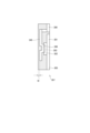
各相の素子配置を図8に示す。図8では、モータリレーモジュール147について、内部構成を模式的に示しており、説明のため、封止部310を梨地で示した。後述の実施形態に係る図も同様である。第1系統におけるU相、V相、W相、および、第2系統におけるU相、V相、W相は、概ね同様の素子配置であるため、主に第1系統のU相を例に説明する。
The arrangement of elements for each phase is shown in Figure 8. In Figure 8, the internal configuration of the
上下アームモジュール141は、平面視略正方形形状に形成されている。モータリレーモジュール147は、長辺の長さが上下アームモジュール141の一辺の長さと概ね同等であり、短辺の長さが上下アームモジュール141の一辺の長さより短い平面視略長方形形状に形成されている。ここで、y方向(すなわち紙面上下方向)を幅方向とすれば、モータリレーモジュール147は、幅狭に形成されている、といえる。
The upper and
モータリレーモジュール147は、短辺側が上下アームモジュール141に向くように、上下アームモジュール141の基板外縁側に隣接して配置されている。本実施形態では、モータリレーモジュール147が上下アームモジュール141より幅狭に形成されているため、上下アームモジュール141をx方向に延長した領域であるモジュール実装領域Rmにモータリレーモジュール147以外の部品を実装可能なスペースを確保可能である。
The
第1系統L1では、モジュール実装領域Rmの基板外縁側において、パワー端部側から、モータリレーモジュール147、スナバ回路素子137、シャント抵抗131の順で配列されている。一方、第2系統L2では、モジュール実装領域Rmの基板外縁側において、制御端部側から、モータリレーモジュール247、スナバ回路素子237、シャント抵抗231の順で配列されている(図7参照)。シャント抵抗131は、長手方向がx方向となるように配置されている。
In the first system L1, the
スナバ回路素子134は、上下アームモジュール141の基板中心線C側であって、抵抗およびコンデンサの長手方向が上下アームモジュール141に向くように、y方向に横並びで配置されている。第1系統L1では、スナバ回路素子134は、モジュール実装領域Rmの基板中心線C側において、制御端部側から、抵抗、コンデンサの順で配列されている。第2系統L2では、スナバ回路素子234は、モジュール実装領域Rmの基板中心線側において、パワー端部側から抵抗、コンデンサの順で配列されている(図7参照)。
The
スナバ回路素子137は、短手方向が上下アームモジュール141に向き、上下アームモジュール141側から、コンデンサ、抵抗の順で配列され、モータリレーモジュール147と隣接して配置されている。
The
モータリレーモジュール147は、ランド301、ドレイン302、ソース303、ゲート304、ドレイン端子305、ソース端子306、ゲート端子307および導電クリップ308等が、封止部310によりモールドされている。
The
モータリレーモジュール147には、一方の短辺に沿ってソース端子306が形成され、他方の短辺に沿ってドレイン端子305およびゲート端子307が形成されている。モータリレーモジュール147は、ソース端子306が上下アームモジュール141側、ドレイン端子305およびゲート端子307が基板外縁側を向くように配置されている。
The
ドレイン端子305は、ランド301と一体に形成されている。ソース303とソース端子306とは、導電クリップ308により接続されている。導電クリップ308は、例えば銅等の電気伝導性のよい材料で形成されており、ワイヤ309より幅広である。ゲート端子307は、ワイヤ309によりゲート304と接続されている。
The
本実施形態では、封止部310の一方の短辺にドレイン端子305およびゲート端子307が形成されており、他方の短辺にソース端子306が形成されている。ドレイン電極がチップ裏面に形成されているのに対し、ソース303はドレイン302より電極面積が小さい。そこで、ゲート端子307をドレイン端子305側に配置してソース端子数をドレイン端子数よりも多くなるようにするとともに、幅広の導電クリップ308にてソース303とソース端子306とを接続している。これにより、ソース側の抵抗を低減可能である。
In this embodiment, the
封止部310は、平面視略長方形形状に形成されている。封止部310の長辺の長さは、短辺の1.5倍以上とすることが望ましい。短辺の長さが長辺の2/3以下、と捉えてもよい。封止部310には、上下アームモジュール141と同様、熱伝導率が比較的高い樹脂が用いられる。熱伝導率は、2.2W/m・K以上であることが好ましい。封止部310として熱伝導率が高い樹脂を用いることで、基板31と反対側の面に露出させることで放熱させる表面電極を省略できるので、モータリレーモジュール147の体格を小型化可能である。
The sealing
図19の参考例に示すように、モータリレーモジュール947のモールド樹脂の熱伝導率が相対的に低く、表面電極948が設けられている場合、上下アームモジュール141よりも厚さが大きくなる。基板31に実装されている素子の厚みに差があると、ヒートシンク945を素子に合わせた形状に形成する必要があり、加工が複雑になる。また、表面電極とヒートシンク945とを絶縁するため、モータリレーモジュール947とヒートシンク945との間に絶縁距離を確保する必要がある。
As shown in the reference example of FIG. 19, when the thermal conductivity of the molded resin of the
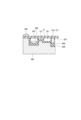
図9に示すように、本実施形態では、モータリレーモジュール147の封止部310として、上下アームモジュール141と同様に熱伝導率が高い樹脂を用い、封止部310から露出する表面電極を設けていない。これにより、上下アームモジュール141とモータリレーモジュール147の厚みを略同じとすることができる。
As shown in FIG. 9, in this embodiment, the sealing
また、上下アームモジュール141およびモータリレーモジュール147と隣接して配置され、基板31と反対への放熱が必要な発熱素子(本実施形態では、シャント抵抗131およびスナバ回路素子134、137)の厚さを、上下アームモジュール141およびモータリレーモジュール147よりも小さく形成している。
In addition, the heat generating elements (in this embodiment, the
これにより、ヒートシンク845との絶縁距離を確保する必要がなく、ヒートシンク845の放熱面848の凹凸を少なくすることができるので、加工が容易になる。なお、図9は、基板31のヒートシンク845側の面における各素子の実装高さを説明するための図であって、実際の配置とは必ずしも一致していない。また、図9および図19において、煩雑になることを避けるため、各素子のハッチングを省略した。
This makes it unnecessary to secure an insulating distance from the
以上説明したように、電子装置30は、上下アームモジュール141~143、241~243と、リレーモジュール147~149、247~249と、周辺部品と、基板31と、を備える。以下、第1系統L1について説明し、第2系統L2について省略する。
As described above, the
上下アームモジュール141~143は、インバータ回路120を構成する同相の上アーム素子121~123および下アーム素子124~126が1つのモジュールとなっている。リレーモジュール147~149は、上下アームモジュール141~143とモータ端子191~193との断接を切替可能なモータリレー素子127~129が素子毎にモジュールとなっている。周辺部品は、シャント抵抗131~133、および、スナバ回路素子134~139の少なくとも一方を含む。基板31には、上下アームモジュール141~143、モータリレーモジュール147~149、および、周辺部品が実装されている。
The upper and lower arm modules 141-143 are formed as one module by the upper arm elements 121-123 and the lower arm elements 124-126 of the same phase that constitute the
基板31の同一面391において、基板中心線Cから外側に向かい、上下アームモジュール141~143、モータリレーモジュール147~149、モータ端子191~193の順に配列されている。また、周辺部品の一部であるシャント抵抗131~133およびスナバ回路素子137~139は、上下アームモジュール141~143とモータ端子191~193との間の領域にて、モータリレーモジュール147~149と横並びに配置されている。これにより、インバータ回路120および周辺回路の基板専有面積を低減することができる。
On the
上下アームモジュール141~143およびモータリレーモジュール147~149において、基板中心線Cに沿う方向(図7等におけるy方向)の長さを幅とすると、モータリレーモジュール147~149は、上下アームモジュール141~143より幅狭である。これにより、モータリレーモジュール147~149の幅方向にて隣接する箇所に、他の部品を実装するスペースを確保することができる。このスペースにシャント抵抗131~133およびスナバ回路素子137~139を配置することで、インバータ回路120および周辺回路の基板専有面積を低減することができる。
In the upper and lower arm modules 141-143 and the motor relay modules 147-149, if the length in the direction along the board center line C (y direction in Figure 7, etc.) is taken as the width, the motor relay modules 147-149 are narrower than the upper and lower arm modules 141-143. This makes it possible to secure space for mounting other components at locations adjacent to the motor relay modules 147-149 in the width direction. By arranging the shunt resistors 131-133 and snubber circuit elements 137-139 in this space, the board area occupied by the
上下アームモジュール141~143およびモータリレーモジュール147~149は、実装高さが等しい。ここで、「実装高さ」とは、基板31に素子を実装したときの高さであって、「実装高さが等しい」とは、基板31に略平行する放熱面848に対して放熱可能であって、放熱ゲル849等にて高さの差を吸収可能な程度の差については許容され、「実装高さが等しい」とみなすものとする。後述の「実装高さ以下」についても同様の程度は許容されるものとする。
The upper and
モータリレーモジュール147~149の基板31と反対側の面は、封止部310で覆われている。図示は省略するが、上下アームモジュール141~143についても同様に、基板31と反対側の面は、封止部で覆われている。換言すると、上下アームモジュール141~143およびモータリレーモジュール147~149は、基板31と反対側の面において、表面電極等の金属が露出していない。本実施形態では、封止部310に熱伝導率の高い樹脂を用いることで、表面電極の露出を行うことなく、高効率に放熱させている。これにより、放熱面848との絶縁距離を確保する必要がないので、放熱面848を凹凸に形成する必要がなく、ヒートシンク845の加工を容易にすることができる。また、絶縁距離の分、上下アームモジュール141~143およびモータリレーモジュール147~149と放熱面848とを離間させる必要がないので、駆動装置1の小型化に寄与する。
The motor relay modules 147-149 are covered with a
シャント抵抗131~133およびスナバ回路素子134~139は、実装高さが上下アームモジュール141~143以下である。これにより、放熱面848に段差を形成する必要がないので、ヒートシンク845の加工を容易にすることができる。
The mounting height of the shunt resistors 131-133 and snubber circuit elements 134-139 is equal to or less than the upper and lower arm modules 141-143. This eliminates the need to form a step on the
上下アームモジュール141~143、モータリレーモジュール147~149、および、シャント抵抗131~133は、基板31の反対側の面からヒートシンク845に放熱可能に設けられている。これにより、通電により生じる熱を適切に放熱させることができる。
The upper and
(第2実施形態)
第2実施形態を図10に示す。第2実施形態~第8実施形態は、主にリレーモジュールが上記実施形態と異なっているので、この点を中心に説明する。
Second Embodiment
The second embodiment is shown in Fig. 10. The second to eighth embodiments are different from the above-mentioned embodiment mainly in the relay module, and therefore this point will be mainly described.
図10に示すように、モータリレーモジュール351は、ランド301、ドレイン302、ソース303、ゲート304、ドレイン端子315、ソース端子316、ゲート端子317および導電クリップ308等が、封止部310によりモールドされている。モータリレーモジュール351では、一方の短辺に沿ってドレイン端子315が形成され、他方の短辺に沿ってソース端子316およびゲート端子317が形成されている。このように構成しても、上記実施形態と同様の効果を奏する。
As shown in FIG. 10, the
(第3実施形態)
第3実施形態を図11に示す。図11に示すモータリレーモジュール352は、ランド301、ドレイン302、ソース303、ゲート304、ドレイン端子315、ソース端子316、ゲート端子317および導電クリップ308等が、封止部310によりモールドされている。図11では、第2実施形態と同様、ゲート端子をソース端子側に配置しているが、第1実施形態と同様、ゲート端子をドレイン端子側に配置してもよい。
Third Embodiment
The third embodiment is shown in Fig. 11. In a
モータリレーモジュール352では、シャント抵抗318、および、シャント抵抗318と接続される基板パターン319を含め、封止部310に一体にモールドされている。すなわち本実施形態では、モータリレーモジュール352には、電流検出に係る素子であるシャント抵抗318が内蔵されている。これにより、シャント抵抗を別体とする場合と比較し、実装面積を低減可能である。また、シャント抵抗318の放熱性を向上可能である。また、上記実施形態と同様の効果を奏する。
In the
(第4実施形態)
第4実施形態を図12に示す。図12に示すリレーモジュール353は、ランド301、ドレイン302、ソース303、ゲート304、ドレイン端子315、ソース端子316、ゲート端子317およびシャント抵抗318等が、封止部310によりモールドされている。
Fourth Embodiment
The fourth embodiment is shown in Fig. 12. In a
本実施形態では、ソース303とソース端子316とを、導電クリップ308に替えて、シャント抵抗318にて接続している。すなわち、シャント抵抗318にて、導電クリップの機能を共用している。これにより、実装面積をより低減可能である。また、上記実施形態と同様の効果を奏する。
In this embodiment, the
(第5実施形態)
第5実施形態を図13に示す。図13に示すモータリレーモジュール354は、ランド301、ドレイン302、ソース303、ゲート304、ドレイン端子315、ソース端子316、ゲート端子317、導電クリップ308、および、放熱端子321等が、封止部310によりモールドされている。
Fifth Embodiment
The fifth embodiment is shown in Fig. 13. In a
放熱端子321は、端子315~317が形成されていない側の辺に沿って形成され、シャント抵抗318と接続される配線パターン322と接続されている。これにより、シャント抵抗318にて発生した熱は、配線パターン322および放熱端子321を経由し、モータリレーモジュール354側からも放熱可能である。
The
本実施形態のモータリレーモジュール354は、シャント抵抗318と接続されている配線パターン322と接続される放熱端子321を有する。これにより、シャント抵抗318にて発生した熱を、より高効率に放熱させることができる。また上記実施形態と同様の効果を奏する。
The
(第6実施形態)
第6実施形態を図14に示す。図14に示すモータリレーモジュール355は、ランド301、ドレイン302、ソース303、ゲート304、ドレイン端子335、ソース端子306、ゲート端子337、導電クリップ308、および、無電位端子338が、封止部310にてモールドされている。
Sixth Embodiment
The sixth embodiment is shown in Fig. 14. In a
本実施形態では、配列されるソース端子306の両側に無電位端子338が設けられており、配列されるドレイン端子335およびゲート端子337の両側に無電位端子338が設けられている。無電位端子338は、例えばゲート端子等の主機能に係る電位が割り当てられていないことを意味し、例えば放熱等の副次的な機能を有していても差し支えない。封止部310の4角に設けられる端子を無電位端子338とすることで、主機能に係る電位が割り当てられている端子のはんだ接合寿命を向上可能である。なお、一部の角部の端子が無電位端子でなくてもよい。
In this embodiment,
また、ゲート端子337の両側には、ドレイン端子335が配置される。これにより、ゲート端子337のはんだ接合寿命を向上可能である。上記実施形態のモータリレーモジュールにおいても、ゲート端子の両側にドレイン端子等の別の端子を配置するようにしてもよい。また、図示は省略するが、上下アームモジュールにおいても、封止部の4角に設けられる端子を無電位端子としてもよい。
In addition,
本実施形態では、モータリレーモジュール355は、矩形に形成されている封止部310の角部の少なくとも1箇所に、無電位端子338が形成されている。これにより、角部にて接合不良が生じたとしても、モータリレーモジュール355の機能を維持可能である。
In this embodiment, the
モータリレーモジュール355において、駆動信号の送受信に係るゲート端子337の両側には、他の端子が配列されている。換言すると、ゲート端子337は、角部に設けられる端子である角ピン以外に割り当てられている。ゲート端子337の両側に配列される端子は、ドレイン端子335に限らず、無電位端子等であってもよい。これにより、角部にて接合不良が生じたとしても、少なくとも駆動信号の送受信を維持可能である。
In the
(第7実施形態)
第7実施形態を図15および図16に示す。図15および図16に示すモータリレーモジュール356は、ランド301、ドレイン302、ソース303、ゲート304、ドレイン端子305、ソース端子306、ゲート端子307および大型導電クリップ341等が、封止部310によりモールドされている。
Seventh Embodiment
The seventh embodiment is shown in Figures 15 and 16. In a
モータリレーモジュール356では、ソース303とソース端子306とが、大型導電クリップ341にて接続されている。例えば第1実施形態の導電クリップ308はソース303より幅狭であるのに対し(図8参照)、大型導電クリップ341は、ソース303より幅広であって、ソース303の全面を覆うように形成されている。本実施形態では、大型導電クリップ341は、ソース端子306からドレイン端子305側まで延びる平板状に形成されており、ゲート304と重複しないように、切り欠かれている。
In the
図16に示すように、大型導電クリップ341は、ソース303側に突出し、ソース303と接続される突出部342を有する。大型導電クリップ341が設けられる箇所の封止部310の厚みである最小厚さHrは、樹脂成形を可能とすべく、モールド樹脂内のフィラー径より厚い。また、最小厚さHrは、スイッチングの耐圧と同等以上の絶縁を確保できる大きさとする。
As shown in FIG. 16, the large
ソース303とソース端子306との接続に大型導電クリップ341を用いることで、ソース側の抵抗を低減することができる。また上記実施形態と同様の効果を奏する。
By using a large
(第8実施形態)
第8実施形態を図17および図18に示す。第8実施形態は、大型導電クリップ345が第7実施形態と異なっているので、この点を中心に説明する。図17および図18に示すように、本実施形態のモータリレーモジュール357では、大型導電クリップ345は、板厚が均一であって、凹部346にて、ソース303と当接する。これにより、均一な板厚の材料を用いて大型導電クリップ345を形成することができる。また、上記実施形態と同様の効果を奏する。
Eighth embodiment
The eighth embodiment is shown in Figures 17 and 18. The eighth embodiment differs from the seventh embodiment in the large
実施形態では、メイン基板31が「基板」、モータリレーモジュール147~149、237~239、351~357が「リレーモジュール」、シャント抵抗131~133、231~233、318が「電流検出素子」および「周辺部品」、スナバ回路素子134~139、234~239が「ノイズ除去素子」および「周辺部品」、モータ端子191~193が「出力端子」、ゲート端子337が「駆動信号端子」に対応する。
In this embodiment, the
(他の実施形態)
上記実施形態では、全てのリレーモジュールにおいて、周辺部品として、シャント抵抗およびスナバ回路素子が横並びに配置されている。他の実施形態では、一部のモータリレーモジュールにおいて、周辺部品が横並びに配置されていなくてもよい。また、他の実施形態では、シャント抵抗またはスナバ回路素子がモータリレーモジュールと横並びに配置されていなくてもよい。また、周辺部品は、シャント抵抗およびスナバ回路素子以外のものであってもよい。また、全てのリレーモジュールが同一の形状である必要はなく、一部のリレーモジュールの形状が他のモジュールと形状が異なっていてもよい。
Other Embodiments
In the above embodiment, in all relay modules, the shunt resistors and snubber circuit elements are arranged side by side as peripheral components. In other embodiments, in some motor relay modules, the peripheral components may not be arranged side by side. In other embodiments, the shunt resistors or snubber circuit elements may not be arranged side by side with the motor relay modules. In addition, the peripheral components may be other than the shunt resistors and snubber circuit elements. In addition, it is not necessary for all relay modules to have the same shape, and the shape of some relay modules may be different from that of other modules.
上記実施形態では、基板に2系統のインバータ回路およびモータリレーモジュール等が実装されている。他の実施形態では、系統数は2系統に限らず、1系統または3系統以上であってもよい。上記実施形態では、電子装置は、モータ駆動回路に適用されている。他の実施形態では、電子装置は発電回路やDCDCコンバータ等、モータ駆動回路以外の回路に適用してもよい。 In the above embodiment, two inverter circuits and a motor relay module are mounted on the board. In other embodiments, the number of systems is not limited to two, and may be one system or three or more systems. In the above embodiment, the electronic device is applied to a motor drive circuit. In other embodiments, the electronic device may be applied to a circuit other than a motor drive circuit, such as a power generation circuit or a DC-DC converter.
上記実施形態では、インバータ回路とマイコンが同一の基板に実装されている。他の実施形態では、インバータ回路とマイコン等の制御に係る電子部品とが異なる基板に実装されていてもよい。また、コネクタ側のサブ基板を省略し、基板が1枚であってもよい。また、基板の枚数等に限らず、駆動回路の構成は上記実施形態とは異なっていてもよい。 In the above embodiment, the inverter circuit and the microcomputer are mounted on the same board. In other embodiments, the inverter circuit and electronic components related to control, such as the microcomputer, may be mounted on different boards. Also, the sub-board on the connector side may be omitted, and there may be only one board. Also, regardless of the number of boards, the configuration of the drive circuit may be different from that of the above embodiment.
上記実施形態では、操舵装置は電動パワーステアリング装置である。他の実施形態では、操舵装置は、ステアバイワイヤ装置であってもよく、駆動装置は、車輪を転舵させる転舵装置として用いてもよいし、ハンドルに反力を付与する反力装置として用いてもよい。また、駆動装置を操舵装置以外の装置に適用してもよい。以上、本発明は、上記実施形態になんら限定されるものではなく、発明の趣旨を逸脱しない範囲において種々の形態で実施可能である。 In the above embodiment, the steering device is an electric power steering device. In other embodiments, the steering device may be a steer-by-wire device, and the drive device may be used as a steering device that steers the wheels, or as a reaction device that applies a reaction force to the steering wheel. The drive device may also be applied to devices other than steering devices. As described above, the present invention is not limited to the above embodiment, and can be implemented in various forms within the scope of the invention.
30・・・電子装置 31・・・メイン基板(基板)
120、220・・・インバータ回路
121~123、221~223・・・上アーム素子
124~126、224~226・・・下アーム素子
127~129、227~229・・・モータリレー素子
131~133、231~233、318・・・シャント抵抗(電流検出素子)
134~139、234~239・・・スナバ回路素子(ノイズ除去素子)
141~143、241~243・・・上下アームモジュール
147~149、247~249、351~357・・・モータリレーモジュール(リレーモジュール)
30: Electronic device 31: Main board (board)
120, 220... inverter circuit 121-123, 221-223... upper arm element 124-126, 224-226... lower arm element 127-129, 227-229... motor relay element 131-133, 231-233, 318... shunt resistor (current detection element)
134 to 139, 234 to 239: snubber circuit elements (noise removal elements)
141-143, 241-243: Upper and lower arm modules 147-149, 247-249, 351-357: Motor relay module (relay module)
Claims (10)
前記上下アームモジュールと出力端子(191~193、291~293)との断接を切替可能なリレー素子(127~129、227~229)が素子毎にモジュールとなっているリレーモジュール(147~149、247~249、351~357)と、
電流検出素子(131~133、231~233)、および、ノイズ除去素子(134~139、234~239)の少なくとも一方を含む周辺部品と、
前記上下アームモジュール、前記リレーモジュール、および、前記周辺部品が実装される基板(31)と、
を備え、
前記基板の同一面(391)において、
基板中心線から外側に向かい、前記上下アームモジュール、前記リレーモジュール、前記出力端子の順で配列されており、
少なくとも一部の前記周辺部品(131~133、137~139、231~233、237~239)は、前記上下アームモジュールと前記出力端子との間の領域にて、前記リレーモジュールと横並びに配置されている電子装置。 upper and lower arm modules (141-143, 241-243) each including upper arm elements (121-123, 221-223) and lower arm elements (124-126, 224-226) of the same phase that constitute an inverter circuit (120, 220) in one module;
relay modules (147-149, 247-249, 351-357) in which relay elements (127-129, 227-229) capable of switching between connection and disconnection of the upper and lower arm modules and output terminals (191-193, 291-293) are formed as modules for each element;
A peripheral component including at least one of a current detection element (131 to 133, 231 to 233) and a noise removal element (134 to 139, 234 to 239);
a substrate (31) on which the upper and lower arm modules, the relay module, and the peripheral components are mounted;
Equipped with
On the same surface (391) of the substrate,
The upper and lower arm modules, the relay modules, and the output terminals are arranged in this order from the center line of the board toward the outside,
An electronic device in which at least some of the peripheral components (131-133, 137-139, 231-233, 237-239) are arranged side by side with the relay module in the area between the upper and lower arm modules and the output terminals.
前記リレーモジュールは、前記上下アームモジュールより幅狭である請求項1に記載の電子装置。 In the upper and lower arm modules and the relay module, when the length in the direction along the board center line is defined as the width,
The electronic device according to claim 1 , wherein the relay module is narrower than the upper and lower arm modules.
Priority Applications (4)
| Application Number | Priority Date | Filing Date | Title |
|---|---|---|---|
| JP2021045122A JP7559638B2 (en) | 2021-03-18 | 2021-03-18 | Electronics |
| PCT/JP2022/010065 WO2022196452A1 (en) | 2021-03-18 | 2022-03-08 | Electronic device |
| CN202280021998.6A CN117015927A (en) | 2021-03-18 | 2022-03-08 | electronic device |
| US18/467,714 US12525891B2 (en) | 2021-03-18 | 2023-09-14 | Electronic device |
Applications Claiming Priority (1)
| Application Number | Priority Date | Filing Date | Title |
|---|---|---|---|
| JP2021045122A JP7559638B2 (en) | 2021-03-18 | 2021-03-18 | Electronics |
Publications (2)
| Publication Number | Publication Date |
|---|---|
| JP2022144211A JP2022144211A (en) | 2022-10-03 |
| JP7559638B2 true JP7559638B2 (en) | 2024-10-02 |
Family
ID=83320434
Family Applications (1)
| Application Number | Title | Priority Date | Filing Date |
|---|---|---|---|
| JP2021045122A Active JP7559638B2 (en) | 2021-03-18 | 2021-03-18 | Electronics |
Country Status (4)
| Country | Link |
|---|---|
| US (1) | US12525891B2 (en) |
| JP (1) | JP7559638B2 (en) |
| CN (1) | CN117015927A (en) |
| WO (1) | WO2022196452A1 (en) |
Families Citing this family (1)
| Publication number | Priority date | Publication date | Assignee | Title |
|---|---|---|---|---|
| JP2025186763A (en) * | 2024-06-12 | 2025-12-24 | 株式会社デンソー | electronic equipment |
Citations (4)
| Publication number | Priority date | Publication date | Assignee | Title |
|---|---|---|---|---|
| JP2016144365A (en) | 2015-02-04 | 2016-08-08 | 新電元工業株式会社 | Semiconductor device |
| WO2018207330A1 (en) | 2017-05-11 | 2018-11-15 | 三菱電機株式会社 | Electric power steering device |
| JP2020188660A (en) | 2019-05-17 | 2020-11-19 | 株式会社デンソー | Electric power conversion device |
| JP2020205663A (en) | 2019-06-14 | 2020-12-24 | 株式会社デンソー | Power supply system |
Family Cites Families (10)
| Publication number | Priority date | Publication date | Assignee | Title |
|---|---|---|---|---|
| EP2228895B1 (en) * | 2009-03-09 | 2012-12-26 | SMA Solar Technology AG | Inverter with utility grid interface |
| EP2695795B1 (en) * | 2011-04-07 | 2019-06-19 | Mitsubishi Electric Corporation | Molded module and electric power steering apparatus |
| JP6160576B2 (en) * | 2014-07-31 | 2017-07-12 | 株式会社デンソー | DRIVE DEVICE AND ELECTRIC POWER STEERING DEVICE USING THE SAME |
| JP6595269B2 (en) | 2015-09-07 | 2019-10-23 | 日立オートモティブシステムズ株式会社 | Electric drive device and electric power steering device |
| CN108966685A (en) * | 2016-03-04 | 2018-12-07 | 日本电产株式会社 | Power inverter, motor drive unit, electric power steering apparatus and relay module |
| JP6838501B2 (en) * | 2017-06-14 | 2021-03-03 | 株式会社デンソー | Electronic control device and electric power steering device using this |
| CN111108668B (en) * | 2017-09-28 | 2022-10-11 | 三菱电机株式会社 | Electric power steering apparatus |
| JP7172849B2 (en) * | 2019-05-17 | 2022-11-16 | 株式会社デンソー | power converter |
| WO2021080016A1 (en) | 2019-10-25 | 2021-04-29 | 株式会社デンソー | Electronic device comprising semiconductor module |
| JP7331827B2 (en) | 2020-12-23 | 2023-08-23 | 株式会社デンソー | Semiconductor package and electronic device using the same |
-
2021
- 2021-03-18 JP JP2021045122A patent/JP7559638B2/en active Active
-
2022
- 2022-03-08 CN CN202280021998.6A patent/CN117015927A/en active Pending
- 2022-03-08 WO PCT/JP2022/010065 patent/WO2022196452A1/en not_active Ceased
-
2023
- 2023-09-14 US US18/467,714 patent/US12525891B2/en active Active
Patent Citations (4)
| Publication number | Priority date | Publication date | Assignee | Title |
|---|---|---|---|---|
| JP2016144365A (en) | 2015-02-04 | 2016-08-08 | 新電元工業株式会社 | Semiconductor device |
| WO2018207330A1 (en) | 2017-05-11 | 2018-11-15 | 三菱電機株式会社 | Electric power steering device |
| JP2020188660A (en) | 2019-05-17 | 2020-11-19 | 株式会社デンソー | Electric power conversion device |
| JP2020205663A (en) | 2019-06-14 | 2020-12-24 | 株式会社デンソー | Power supply system |
Also Published As
| Publication number | Publication date |
|---|---|
| JP2022144211A (en) | 2022-10-03 |
| CN117015927A (en) | 2023-11-07 |
| US20240007016A1 (en) | 2024-01-04 |
| WO2022196452A1 (en) | 2022-09-22 |
| US12525891B2 (en) | 2026-01-13 |
Similar Documents
| Publication | Publication Date | Title |
|---|---|---|
| JP6680054B2 (en) | Drive device and electric power steering device using the same | |
| JP5725055B2 (en) | Electronic control unit | |
| US8456049B2 (en) | Drive apparatus | |
| JP6680053B2 (en) | Drive device and electric power steering device using the same | |
| CN108137084B (en) | Integrated electric power steering device and manufacturing method thereof | |
| US9000633B2 (en) | Drive apparatus having a motor, a heat sink, and a plurality of semiconductor modules | |
| JP7067339B2 (en) | Drive device and electric power steering device using this | |
| JP4957815B2 (en) | Semiconductor module and motor with built-in electronic circuit using the same | |
| JP5067679B2 (en) | Semiconductor module and driving device using the same | |
| JP7004289B2 (en) | Motor control device and electric power steering device | |
| US20130119908A1 (en) | Electronic control unit for electric power steering | |
| US8520394B2 (en) | Control device | |
| US8796971B2 (en) | Motor drive apparatus | |
| JP5572577B2 (en) | Electronic control unit for electric motor | |
| WO2016163037A1 (en) | Electric power steering device | |
| JP2012239295A (en) | Drive device | |
| JP7328792B2 (en) | drive | |
| JP2014183615A (en) | Rotary electric machine | |
| JP7683259B2 (en) | Drive unit | |
| JP7559638B2 (en) | Electronics | |
| JP5485591B2 (en) | Drive device and semiconductor module | |
| JP7608901B2 (en) | Semiconductor module and electronic device using same | |
| WO2026034412A1 (en) | Electronic device |
Legal Events
| Date | Code | Title | Description |
|---|---|---|---|
| A621 | Written request for application examination |
Free format text: JAPANESE INTERMEDIATE CODE: A621 Effective date: 20230907 |
|
| TRDD | Decision of grant or rejection written | ||
| A01 | Written decision to grant a patent or to grant a registration (utility model) |
Free format text: JAPANESE INTERMEDIATE CODE: A01 Effective date: 20240820 |
|
| A61 | First payment of annual fees (during grant procedure) |
Free format text: JAPANESE INTERMEDIATE CODE: A61 Effective date: 20240902 |
|
| R150 | Certificate of patent or registration of utility model |
Ref document number: 7559638 Country of ref document: JP Free format text: JAPANESE INTERMEDIATE CODE: R150 |