JP7560247B2 - エレクトロルミネセント表示パネル、及び表示装置 - Google Patents
エレクトロルミネセント表示パネル、及び表示装置 Download PDFInfo
- Publication number
- JP7560247B2 JP7560247B2 JP2019569405A JP2019569405A JP7560247B2 JP 7560247 B2 JP7560247 B2 JP 7560247B2 JP 2019569405 A JP2019569405 A JP 2019569405A JP 2019569405 A JP2019569405 A JP 2019569405A JP 7560247 B2 JP7560247 B2 JP 7560247B2
- Authority
- JP
- Japan
- Prior art keywords
- color subpixel
- substrate
- onto
- orthogonal projection
- color
- Prior art date
- Legal status (The legal status is an assumption and is not a legal conclusion. Google has not performed a legal analysis and makes no representation as to the accuracy of the status listed.)
- Active
Links
Images



Classifications
-
- G—PHYSICS
- G02—OPTICS
- G02F—OPTICAL DEVICES OR ARRANGEMENTS FOR THE CONTROL OF LIGHT BY MODIFICATION OF THE OPTICAL PROPERTIES OF THE MEDIA OF THE ELEMENTS INVOLVED THEREIN; NON-LINEAR OPTICS; FREQUENCY-CHANGING OF LIGHT; OPTICAL LOGIC ELEMENTS; OPTICAL ANALOGUE/DIGITAL CONVERTERS
- G02F1/00—Devices or arrangements for the control of the intensity, colour, phase, polarisation or direction of light arriving from an independent light source, e.g. switching, gating or modulating; Non-linear optics
- G02F1/01—Devices or arrangements for the control of the intensity, colour, phase, polarisation or direction of light arriving from an independent light source, e.g. switching, gating or modulating; Non-linear optics for the control of the intensity, phase, polarisation or colour
- G02F1/13—Devices or arrangements for the control of the intensity, colour, phase, polarisation or direction of light arriving from an independent light source, e.g. switching, gating or modulating; Non-linear optics for the control of the intensity, phase, polarisation or colour based on liquid crystals, e.g. single liquid crystal display cells
- G02F1/133—Constructional arrangements; Operation of liquid crystal cells; Circuit arrangements
- G02F1/1333—Constructional arrangements; Manufacturing methods
- G02F1/1343—Electrodes
- G02F1/134309—Electrodes characterised by their geometrical arrangement
-
- H—ELECTRICITY
- H10—SEMICONDUCTOR DEVICES; ELECTRIC SOLID-STATE DEVICES NOT OTHERWISE PROVIDED FOR
- H10K—ORGANIC ELECTRIC SOLID-STATE DEVICES
- H10K50/00—Organic light-emitting devices
- H10K50/80—Constructional details
- H10K50/805—Electrodes
- H10K50/81—Anodes
- H10K50/814—Anodes combined with auxiliary electrodes, e.g. ITO layer combined with metal lines
-
- G—PHYSICS
- G09—EDUCATION; CRYPTOGRAPHY; DISPLAY; ADVERTISING; SEALS
- G09G—ARRANGEMENTS OR CIRCUITS FOR CONTROL OF INDICATING DEVICES USING STATIC MEANS TO PRESENT VARIABLE INFORMATION
- G09G3/00—Control arrangements or circuits, of interest only in connection with visual indicators other than cathode-ray tubes
- G09G3/20—Control arrangements or circuits, of interest only in connection with visual indicators other than cathode-ray tubes for presentation of an assembly of a number of characters, e.g. a page, by composing the assembly by combination of individual elements arranged in a matrix no fixed position being assigned to or needed to be assigned to the individual characters or partial characters
- G09G3/22—Control arrangements or circuits, of interest only in connection with visual indicators other than cathode-ray tubes for presentation of an assembly of a number of characters, e.g. a page, by composing the assembly by combination of individual elements arranged in a matrix no fixed position being assigned to or needed to be assigned to the individual characters or partial characters using controlled light sources
- G09G3/30—Control arrangements or circuits, of interest only in connection with visual indicators other than cathode-ray tubes for presentation of an assembly of a number of characters, e.g. a page, by composing the assembly by combination of individual elements arranged in a matrix no fixed position being assigned to or needed to be assigned to the individual characters or partial characters using controlled light sources using electroluminescent panels
- G09G3/32—Control arrangements or circuits, of interest only in connection with visual indicators other than cathode-ray tubes for presentation of an assembly of a number of characters, e.g. a page, by composing the assembly by combination of individual elements arranged in a matrix no fixed position being assigned to or needed to be assigned to the individual characters or partial characters using controlled light sources using electroluminescent panels semiconductive, e.g. using light-emitting diodes [LED]
- G09G3/3208—Control arrangements or circuits, of interest only in connection with visual indicators other than cathode-ray tubes for presentation of an assembly of a number of characters, e.g. a page, by composing the assembly by combination of individual elements arranged in a matrix no fixed position being assigned to or needed to be assigned to the individual characters or partial characters using controlled light sources using electroluminescent panels semiconductive, e.g. using light-emitting diodes [LED] organic, e.g. using organic light-emitting diodes [OLED]
-
- G—PHYSICS
- G09—EDUCATION; CRYPTOGRAPHY; DISPLAY; ADVERTISING; SEALS
- G09G—ARRANGEMENTS OR CIRCUITS FOR CONTROL OF INDICATING DEVICES USING STATIC MEANS TO PRESENT VARIABLE INFORMATION
- G09G3/00—Control arrangements or circuits, of interest only in connection with visual indicators other than cathode-ray tubes
- G09G3/20—Control arrangements or circuits, of interest only in connection with visual indicators other than cathode-ray tubes for presentation of an assembly of a number of characters, e.g. a page, by composing the assembly by combination of individual elements arranged in a matrix no fixed position being assigned to or needed to be assigned to the individual characters or partial characters
- G09G3/22—Control arrangements or circuits, of interest only in connection with visual indicators other than cathode-ray tubes for presentation of an assembly of a number of characters, e.g. a page, by composing the assembly by combination of individual elements arranged in a matrix no fixed position being assigned to or needed to be assigned to the individual characters or partial characters using controlled light sources
- G09G3/30—Control arrangements or circuits, of interest only in connection with visual indicators other than cathode-ray tubes for presentation of an assembly of a number of characters, e.g. a page, by composing the assembly by combination of individual elements arranged in a matrix no fixed position being assigned to or needed to be assigned to the individual characters or partial characters using controlled light sources using electroluminescent panels
- G09G3/32—Control arrangements or circuits, of interest only in connection with visual indicators other than cathode-ray tubes for presentation of an assembly of a number of characters, e.g. a page, by composing the assembly by combination of individual elements arranged in a matrix no fixed position being assigned to or needed to be assigned to the individual characters or partial characters using controlled light sources using electroluminescent panels semiconductive, e.g. using light-emitting diodes [LED]
- G09G3/3208—Control arrangements or circuits, of interest only in connection with visual indicators other than cathode-ray tubes for presentation of an assembly of a number of characters, e.g. a page, by composing the assembly by combination of individual elements arranged in a matrix no fixed position being assigned to or needed to be assigned to the individual characters or partial characters using controlled light sources using electroluminescent panels semiconductive, e.g. using light-emitting diodes [LED] organic, e.g. using organic light-emitting diodes [OLED]
- G09G3/3225—Control arrangements or circuits, of interest only in connection with visual indicators other than cathode-ray tubes for presentation of an assembly of a number of characters, e.g. a page, by composing the assembly by combination of individual elements arranged in a matrix no fixed position being assigned to or needed to be assigned to the individual characters or partial characters using controlled light sources using electroluminescent panels semiconductive, e.g. using light-emitting diodes [LED] organic, e.g. using organic light-emitting diodes [OLED] using an active matrix
-
- G—PHYSICS
- G09—EDUCATION; CRYPTOGRAPHY; DISPLAY; ADVERTISING; SEALS
- G09G—ARRANGEMENTS OR CIRCUITS FOR CONTROL OF INDICATING DEVICES USING STATIC MEANS TO PRESENT VARIABLE INFORMATION
- G09G3/00—Control arrangements or circuits, of interest only in connection with visual indicators other than cathode-ray tubes
- G09G3/20—Control arrangements or circuits, of interest only in connection with visual indicators other than cathode-ray tubes for presentation of an assembly of a number of characters, e.g. a page, by composing the assembly by combination of individual elements arranged in a matrix no fixed position being assigned to or needed to be assigned to the individual characters or partial characters
- G09G3/22—Control arrangements or circuits, of interest only in connection with visual indicators other than cathode-ray tubes for presentation of an assembly of a number of characters, e.g. a page, by composing the assembly by combination of individual elements arranged in a matrix no fixed position being assigned to or needed to be assigned to the individual characters or partial characters using controlled light sources
- G09G3/30—Control arrangements or circuits, of interest only in connection with visual indicators other than cathode-ray tubes for presentation of an assembly of a number of characters, e.g. a page, by composing the assembly by combination of individual elements arranged in a matrix no fixed position being assigned to or needed to be assigned to the individual characters or partial characters using controlled light sources using electroluminescent panels
- G09G3/32—Control arrangements or circuits, of interest only in connection with visual indicators other than cathode-ray tubes for presentation of an assembly of a number of characters, e.g. a page, by composing the assembly by combination of individual elements arranged in a matrix no fixed position being assigned to or needed to be assigned to the individual characters or partial characters using controlled light sources using electroluminescent panels semiconductive, e.g. using light-emitting diodes [LED]
- G09G3/3208—Control arrangements or circuits, of interest only in connection with visual indicators other than cathode-ray tubes for presentation of an assembly of a number of characters, e.g. a page, by composing the assembly by combination of individual elements arranged in a matrix no fixed position being assigned to or needed to be assigned to the individual characters or partial characters using controlled light sources using electroluminescent panels semiconductive, e.g. using light-emitting diodes [LED] organic, e.g. using organic light-emitting diodes [OLED]
- G09G3/3225—Control arrangements or circuits, of interest only in connection with visual indicators other than cathode-ray tubes for presentation of an assembly of a number of characters, e.g. a page, by composing the assembly by combination of individual elements arranged in a matrix no fixed position being assigned to or needed to be assigned to the individual characters or partial characters using controlled light sources using electroluminescent panels semiconductive, e.g. using light-emitting diodes [LED] organic, e.g. using organic light-emitting diodes [OLED] using an active matrix
- G09G3/3233—Control arrangements or circuits, of interest only in connection with visual indicators other than cathode-ray tubes for presentation of an assembly of a number of characters, e.g. a page, by composing the assembly by combination of individual elements arranged in a matrix no fixed position being assigned to or needed to be assigned to the individual characters or partial characters using controlled light sources using electroluminescent panels semiconductive, e.g. using light-emitting diodes [LED] organic, e.g. using organic light-emitting diodes [OLED] using an active matrix with pixel circuitry controlling the current through the light-emitting element
-
- H—ELECTRICITY
- H10—SEMICONDUCTOR DEVICES; ELECTRIC SOLID-STATE DEVICES NOT OTHERWISE PROVIDED FOR
- H10D—INORGANIC ELECTRIC SEMICONDUCTOR DEVICES
- H10D86/00—Integrated devices formed in or on insulating or conducting substrates, e.g. formed in silicon-on-insulator [SOI] substrates or on stainless steel or glass substrates
- H10D86/40—Integrated devices formed in or on insulating or conducting substrates, e.g. formed in silicon-on-insulator [SOI] substrates or on stainless steel or glass substrates characterised by multiple TFTs
- H10D86/441—Interconnections, e.g. scanning lines
-
- H—ELECTRICITY
- H10—SEMICONDUCTOR DEVICES; ELECTRIC SOLID-STATE DEVICES NOT OTHERWISE PROVIDED FOR
- H10D—INORGANIC ELECTRIC SEMICONDUCTOR DEVICES
- H10D86/00—Integrated devices formed in or on insulating or conducting substrates, e.g. formed in silicon-on-insulator [SOI] substrates or on stainless steel or glass substrates
- H10D86/40—Integrated devices formed in or on insulating or conducting substrates, e.g. formed in silicon-on-insulator [SOI] substrates or on stainless steel or glass substrates characterised by multiple TFTs
- H10D86/481—Integrated devices formed in or on insulating or conducting substrates, e.g. formed in silicon-on-insulator [SOI] substrates or on stainless steel or glass substrates characterised by multiple TFTs integrated with passive devices, e.g. auxiliary capacitors
-
- H—ELECTRICITY
- H10—SEMICONDUCTOR DEVICES; ELECTRIC SOLID-STATE DEVICES NOT OTHERWISE PROVIDED FOR
- H10D—INORGANIC ELECTRIC SEMICONDUCTOR DEVICES
- H10D86/00—Integrated devices formed in or on insulating or conducting substrates, e.g. formed in silicon-on-insulator [SOI] substrates or on stainless steel or glass substrates
- H10D86/40—Integrated devices formed in or on insulating or conducting substrates, e.g. formed in silicon-on-insulator [SOI] substrates or on stainless steel or glass substrates characterised by multiple TFTs
- H10D86/60—Integrated devices formed in or on insulating or conducting substrates, e.g. formed in silicon-on-insulator [SOI] substrates or on stainless steel or glass substrates characterised by multiple TFTs wherein the TFTs are in active matrices
-
- H—ELECTRICITY
- H10—SEMICONDUCTOR DEVICES; ELECTRIC SOLID-STATE DEVICES NOT OTHERWISE PROVIDED FOR
- H10K—ORGANIC ELECTRIC SOLID-STATE DEVICES
- H10K59/00—Integrated devices, or assemblies of multiple devices, comprising at least one organic light-emitting element covered by group H10K50/00
- H10K59/10—OLED displays
- H10K59/12—Active-matrix OLED [AMOLED] displays
- H10K59/121—Active-matrix OLED [AMOLED] displays characterised by the geometry or disposition of pixel elements
- H10K59/1213—Active-matrix OLED [AMOLED] displays characterised by the geometry or disposition of pixel elements the pixel elements being TFTs
-
- H—ELECTRICITY
- H10—SEMICONDUCTOR DEVICES; ELECTRIC SOLID-STATE DEVICES NOT OTHERWISE PROVIDED FOR
- H10K—ORGANIC ELECTRIC SOLID-STATE DEVICES
- H10K59/00—Integrated devices, or assemblies of multiple devices, comprising at least one organic light-emitting element covered by group H10K50/00
- H10K59/10—OLED displays
- H10K59/12—Active-matrix OLED [AMOLED] displays
- H10K59/121—Active-matrix OLED [AMOLED] displays characterised by the geometry or disposition of pixel elements
- H10K59/1216—Active-matrix OLED [AMOLED] displays characterised by the geometry or disposition of pixel elements the pixel elements being capacitors
-
- H—ELECTRICITY
- H10—SEMICONDUCTOR DEVICES; ELECTRIC SOLID-STATE DEVICES NOT OTHERWISE PROVIDED FOR
- H10K—ORGANIC ELECTRIC SOLID-STATE DEVICES
- H10K59/00—Integrated devices, or assemblies of multiple devices, comprising at least one organic light-emitting element covered by group H10K50/00
- H10K59/10—OLED displays
- H10K59/12—Active-matrix OLED [AMOLED] displays
- H10K59/123—Connection of the pixel electrodes to the thin film transistors [TFT]
-
- H—ELECTRICITY
- H10—SEMICONDUCTOR DEVICES; ELECTRIC SOLID-STATE DEVICES NOT OTHERWISE PROVIDED FOR
- H10K—ORGANIC ELECTRIC SOLID-STATE DEVICES
- H10K59/00—Integrated devices, or assemblies of multiple devices, comprising at least one organic light-emitting element covered by group H10K50/00
- H10K59/10—OLED displays
- H10K59/12—Active-matrix OLED [AMOLED] displays
- H10K59/131—Interconnections, e.g. wiring lines or terminals
-
- H—ELECTRICITY
- H10—SEMICONDUCTOR DEVICES; ELECTRIC SOLID-STATE DEVICES NOT OTHERWISE PROVIDED FOR
- H10K—ORGANIC ELECTRIC SOLID-STATE DEVICES
- H10K59/00—Integrated devices, or assemblies of multiple devices, comprising at least one organic light-emitting element covered by group H10K50/00
- H10K59/30—Devices specially adapted for multicolour light emission
- H10K59/35—Devices specially adapted for multicolour light emission comprising red-green-blue [RGB] subpixels
- H10K59/351—Devices specially adapted for multicolour light emission comprising red-green-blue [RGB] subpixels comprising more than three subpixels, e.g. red-green-blue-white [RGBW]
-
- H—ELECTRICITY
- H10—SEMICONDUCTOR DEVICES; ELECTRIC SOLID-STATE DEVICES NOT OTHERWISE PROVIDED FOR
- H10K—ORGANIC ELECTRIC SOLID-STATE DEVICES
- H10K59/00—Integrated devices, or assemblies of multiple devices, comprising at least one organic light-emitting element covered by group H10K50/00
- H10K59/30—Devices specially adapted for multicolour light emission
- H10K59/35—Devices specially adapted for multicolour light emission comprising red-green-blue [RGB] subpixels
- H10K59/352—Devices specially adapted for multicolour light emission comprising red-green-blue [RGB] subpixels the areas of the RGB subpixels being different
-
- H—ELECTRICITY
- H10—SEMICONDUCTOR DEVICES; ELECTRIC SOLID-STATE DEVICES NOT OTHERWISE PROVIDED FOR
- H10K—ORGANIC ELECTRIC SOLID-STATE DEVICES
- H10K59/00—Integrated devices, or assemblies of multiple devices, comprising at least one organic light-emitting element covered by group H10K50/00
- H10K59/30—Devices specially adapted for multicolour light emission
- H10K59/35—Devices specially adapted for multicolour light emission comprising red-green-blue [RGB] subpixels
- H10K59/353—Devices specially adapted for multicolour light emission comprising red-green-blue [RGB] subpixels characterised by the geometrical arrangement of the RGB subpixels
-
- H—ELECTRICITY
- H10—SEMICONDUCTOR DEVICES; ELECTRIC SOLID-STATE DEVICES NOT OTHERWISE PROVIDED FOR
- H10K—ORGANIC ELECTRIC SOLID-STATE DEVICES
- H10K71/00—Manufacture or treatment specially adapted for the organic devices covered by this subclass
Landscapes
- Engineering & Computer Science (AREA)
- Physics & Mathematics (AREA)
- Microelectronics & Electronic Packaging (AREA)
- General Physics & Mathematics (AREA)
- Geometry (AREA)
- Computer Hardware Design (AREA)
- Theoretical Computer Science (AREA)
- Optics & Photonics (AREA)
- Nonlinear Science (AREA)
- Mathematical Physics (AREA)
- Chemical & Material Sciences (AREA)
- Crystallography & Structural Chemistry (AREA)
- Manufacturing & Machinery (AREA)
- Electroluminescent Light Sources (AREA)
- Devices For Indicating Variable Information By Combining Individual Elements (AREA)
- Control Of El Displays (AREA)
Description
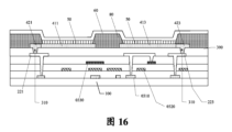
前記2番目の第2色サブ画素において、前記第2のビアは、前記第1のビアにおける前記主体部分から離れる側に位置する。
20 画素駆動回路
21 接続線
30 平坦層
31 ビア
40 陽極
50 発光層
60 陰極
80 画素限定層
90 有効発光領域
100 基板
200 第1の導電層
210 第1の電源線
211 複数のサブ電源線
212 導線
220、221、2221、2222、223 第1の接続線
230 データ線
240 ブリッジング線
300 第1の絶縁層
310 第1のビア
341a、342a、343a、351a 接続部
381a、382a、3831a、3832a、384a、385a、386a、387a、388a ビア
351a 接続部
400 陽極
410、411、413、4121、4122 主体部分
420、421,423、4221、4222 補助部分
500 第2の絶縁層
520 第2のビア
530 第3のビア
610 第2の電源線
620、621、6221、6222、623 第2の接続線
710 第4のビア
001 重複ユニット
010 第1色サブ画素
020 第2色サブ画素対
021、022 第2色サブ画素
030 第3色サブ画素
0120 発光元件
0121 画素駆動回路
0122 画素駆動回路
0123 第1の発光制御回路
0124 第2の発光制御回路
0126 データ書込回路
0127 記憶回路
0128 閾値補償回路
0129 リセット回路
0310 アクティブ半導体層
0320 ゲート導電層
0330 基準導電層
0340 ソース・ドレイン金属層
0350 補助金属層
Claims (25)
- それぞれ複数のサブ画素を含む複数の重複ユニットを備え、
各前記サブ画素は、
基板に位置する第1の導電層と、
前記第1の導電層における前記基板から離れる一側に位置し、前記第1の導電層の一部を露出させる第1のビアを含む、第1の絶縁層と、
前記第1の絶縁層の前記第1の導電層から離れる一側に位置し、互いに電気的に接続された主体部分と補助部分とを含み、前記補助部分は前記第1のビアを介して前記第1の導電層に電気的に接続される、陽極と、を含み、
少なくとも1つの前記サブ画素において、前記基板への前記主体部分の正投影と、前記基板への前記第1のビアの正投影とは重ならなく、
少なくとも1つの前記サブ画素において、前記主体部分の第1方向のサイズは前記主体部分の第2方向のサイズよりも大きく、且つ、少なくとも1つの前記サブ画素において、前記第1のビアと前記主体部分とは前記第2方向に沿って配置され、ここで、前記第1方向と前記第2方向とは互いに異なり、
前記複数の重複ユニットにおける少なくとも1つの重複ユニットは、前記第2方向に沿って配列された1つの第1色サブ画素と、1つの第2色サブ画素対と、1つの第3色サブ画素と、を含み、ここで、前記第2色サブ画素対は、前記第1方向に沿って配列された2つの第2色サブ画素を含み、
前記複数の重複ユニットは前記第2方向に沿って配列されて重複ユニットグループを形成し、前記重複ユニットグループは前記第1方向に沿って配列され、且つ、隣接する2つの前記重複ユニットグループにおける重複ユニットは位置がずれて配列され、
各前記サブ画素は、前記第1の導電層において前記基板に面する側に位置する画素駆動回路をさらに含み、ここで、各前記サブ画素において、画素駆動回路がアレイで分布され、
前記第1色サブ画素の主体部分の前記第1方向の延在方向と、前記第1色サブ画素の画素駆動回路における各層パターンが存在する領域の前記第2方向の長さ方向との間は、第1の夾角があり、ここで、前記第1の夾角は、45度ないし165度の間にあり、
前記第3色サブ画素の主体部分の前記第1方向の延在方向と、前記第3色サブ画素の画素駆動回路における各層パターンが存在する領域の前記第2方向の長さ方向との間は、第2の夾角があり、ここで、前記第2の夾角は、45度ないし165度の間にあり、
前記第2色サブ画素対の前記第1方向の延在方向と、第2色サブ画素対の画素駆動回路における各層パターンが存在する領域の前記第2方向の長さ方向との間は、第3の夾角があり、ここで、前記第3の夾角は、45度ないし165度の間にあり、
各前記サブ画素の前記画素駆動回路が位置する領域は、長方形であり、前記長さ方向は、前記長方形の長辺が延在する方向であり、
前記第3色サブ画素において、前記基板への前記主体部分の正投影と、前記基板への前記画素駆動回路における駆動トランジスタの正投影とは重ならなく、前記基板への前記主体部分の正投影と、前記基板への、前記第2方向において前記画素駆動回路に隣接する画素駆動回路に電気的に接続されたリセット制御信号線およびリセット電源信号線の正投影とは重なり、前記基板への前記主体部分の正投影と前記基板への2つのデータ線の正投影とは重なり、前記基板への前記主体部分の正投影と前記基板への2つのサブ電源線の正投影とは重なる、エレクトロルミネセント表示パネル。 - 前記第1の導電層は、互いに間隔して設置された第1の電源線と第1の接続線とを含み、
各前記サブ画素において、前記補助部分は前記第1のビアを介して前記第1の接続線に電気的に接続される、請求項1に記載のエレクトロルミネセント表示パネル。 - 前記第1の電源線は、前記第1方向に沿って配列され、且つ、前記第2方向に沿って延びる複数のサブ電源線と、各々の前記サブ電源線を電気的に接続させる導線と、を含み、
前記サブ電源線と前記導線とはグリッド状な構成を形成し、それぞれのグリッド内部には1つの前記第1の接続線が設置されており、且つ、前記第1の接続線と前記サブ電源線及び前記導線のいずれとの間にも間隔がある、請求項2に記載のエレクトロルミネセント表示パネル。 - 各前記画素駆動回路における各層パターンが存在する領域の前記第2方向のサイズは、第1方向のサイズよりも大きく、
前記第1色サブ画素の主体部分の前記第2方向のサイズは、前記第3色サブ画素の主体部分の前記第2方向のサイズよりも小さく、
前記第1色サブ画素の主体部分の前記第1方向のサイズは、前記第3色サブ画素の主体部分の前記第1方向のサイズよりも大きい、請求項3に記載のエレクトロルミネセント表示パネル。 - 各前記第3色サブ画素において、前記基板への前記主体部分の正投影と前記基板への前記第1のビアの正投影とは重ならなく、
ここで、各前記第1色サブ画素において、前記基板への前記主体部分の正投影と前記基板への前記第1のビアの正投影とは重ならなく、
各前記第2色サブ画素において、前記基板への前記主体部分の正投影と前記基板への前記第1のビアの正投影とは重ならない、請求項3又は4に記載のエレクトロルミネセント表示パネル。 - 前記第3色サブ画素において、前記主体部分は軸対称図形であり、且つ、前記第1のビアは前記第2方向に沿う前記主体部分の対称軸に位置し、
前記第1色サブ画素において、前記主体部分は軸対称図形であり、且つ、前記第1のビアは前記第2方向に沿う前記主体部分の対称軸に位置し、
前記第1色サブ画素において、前記基板への前記主体部分の正投影と前記画素駆動回路における駆動トランジスタとは重なり、前記基板への前記主体部分の正投影と、前記基板への前記画素駆動回路に電気的に接続された発光制御信号線の正投影とは重なり、前記基板への前記主体部分の正投影と前記基板への2つのデータ線の正投影とは重なり、前記基板への前記主体部分の正投影と前記基板への2つの第2の電源線の正投影とは重なる、請求項5に記載のエレクトロルミネセント表示パネル。 - 前記第2色サブ画素対は、1番目の第2色サブ画素と2番目の第2色サブ画素とを含み、同一の前記重複ユニットにおいて、前記1番目の第2色サブ画素の第1のビアは、前記1番目の第2色サブ画素における前記第3色サブ画素から離れる側に位置し、
同一の前記重複ユニットにおいて、前記2番目の第2色サブ画素の第1のビアは、前記2番目の第2色サブ画素における前記第3色サブ画素から離れる側に位置する、請求項5に記載のエレクトロルミネセント表示パネル。 - 同一の重複ユニットにおける第1色サブ画素と前記1番目の第2色サブ画素、および、前記同一の重複ユニットにおける第1色サブ画素及び前記1番目の第2色サブ画素のいずれにも最も近い第3色サブ画素について、前記1番目の第2色サブ画素の第1のビアは、前記第1色サブ画素と前記第3色サブ画素との間の隙間に位置し、
同一の重複ユニットにおける第1色サブ画素と2番目の第2色サブ画素、および、前記同一の重複ユニットにおける第1色サブ画素及び2番目の第2色サブ画素のいずれにも最も近い第3色サブ画素について、前記2番目の第2色サブ画素の第1のビアは、前記第1色サブ画素と前記第3色サブ画素との間の隙間に位置する、請求項7に記載のエレクトロルミネセント表示パネル。 - 前記1番目の第2色サブ画素において、前記基板への前記主体部分の正投影と前記基板への前記画素駆動回路における駆動トランジスタの正投影とは重ならなく、前記基板への前記主体部分の正投影と、前記基板への、前記第2方向において前記画素駆動回路に隣接する画素駆動回路に電気的に接続されたリセット制御信号線および走査信号線の正投影とは重なり、
前記2番目の第2色サブ画素において、前記基板への前記主体部分の正投影と前記基板への前記画素駆動回路における駆動トランジスタの正投影とは重ならなく、前記基板への前記主体部分の正投影と、前記基板への、前記第2方向において前記画素駆動回路に隣接する画素駆動回路に電気的に接続されたリセット制御信号線および走査信号線の正投影とは重なる、請求項7に記載のエレクトロルミネセント表示パネル。 - 前記第3色サブ画素における画素駆動回路、前記1番目の第2色サブ画素における画素駆動回路、前記第1色サブ画素における画素駆動回路、および、前記2番目の第2色サブ画素における画素駆動回路は、前記第1方向に沿って順次に配置される、請求項7~9のいずれか一項に記載のエレクトロルミネセント表示パネル。
- 同種の色のサブ画素における第1のビアは、前記同種の色のサブ画素の同一側に位置する、請求項1~10のいずれか一項に記載のエレクトロルミネセント表示パネル。
- 同一の前記重複ユニットにおいて、前記1番目の第2色サブ画素の第1のビア、前記第1色サブ画素の第1のビア、および、前記2番目の第2色サブ画素の第1のビアは、前記第1方向に沿って、同一の第1の線分に順に配列され、
1つの重複ユニットグループにおける1つの第2色サブ画素、および、隣接する重複ユニットグループにおける1つの前記第2色サブ画素に最も近い第3色サブ画素について、前記1つの第2色サブ画素の第1のビアおよび前記第3色サブ画素の第1のビアは、第3の方向に沿って同一の第2の線分に配列され、ここで、前記第3の方向と前記第1方向とは交差し、
隣接する重複ユニットグループにそれぞれ位置する、隣接する2つの重複ユニットにおいて、1番目の重複ユニットにおける第3色サブ画素の第1のビアと2番目の重複ユニットにおける前記1番目の第2色サブ画素の第1のビア、前記第1色サブ画素の第1のビア、および、前記2番目の第2色サブ画素の第1のビアは、この順に前記第1の線分と前記第2の線分が接続した折れ線に配列される、請求項7に記載のエレクトロルミネセント表示パネル。 - 同一の前記重複ユニットにおける前記第3色サブ画素の第1のビア、および、前記第1色サブ画素の第1のビアは、前記第2方向に沿って同一の直線に配列され、
隣接する重複ユニットグループにそれぞれ位置し、且つ、隣接する2つの重複ユニットにおいて、1つの重複ユニットにおける前記1番目の第2色サブ画素の第1のビア、および、他の1つの重複ユニットにおける前記2番目の第2色サブ画素の第1のビアは、前記第2方向に沿って同一の直線に配列され、
奇数の重複ユニットグループおよび偶数類の重複ユニットグループにおける少なくとも1類の重複ユニットグループにおいて、前記第1方向に配列される前記第1色サブ画素の第1のビア、前記第2色サブ画素対における前記1番目の第2色サブ画素の第1のビア、および、前記2番目の第2色サブ画素の第1のビアは、前記第1方向に沿って同一の直線に配列され、
また、奇数の重複ユニットグループおよび偶数の重複ユニットグループにおける少なくとも1類の重複ユニットグループにおいて、前記第1方向に配列される前記第3色サブ画素の第1のビアは、前記第1方向に沿って同一の直線に配列される、請求項12に記載のエレクトロルミネセント表示パネル。 - 前記第1の導電層と前記基板との間に位置し、間隔して設置された第2の電源線と第2の接続線とを含む、第2の導電層と、
前記第2の導電層と前記第1の導電層との間に位置し、前記第2の接続線を露出させる第2のビアと前記第2の電源線の一部を露出させる第3のビアとを有する、第2の絶縁層と、をさらに含み、
前記第1の接続線は、前記第2のビアと前記第2の接続線とを介して互いに電気的に接続され、
前記第1の電源線は、前記第3のビアと前記第2の電源線とを介して互いに電気的に接続され、
互いに電気的に接続された前記第1の接続線と前記第2の接続線について、前記基板への前記第1の接続線の正投影と前記基板への前記第2の接続線の正投影とは少なくとも一部が重なり、
前記基板への前記第1の電源線の正投影と前記基板への前記第2の電源線の正投影とは少なくとも一部が重なり、
前記第3色サブ画素において、前記第1のビアは、前記第2のビアよりも前記画素駆動回路における駆動トランジスタに接近して設置され、
前記第1色サブ画素において、前記第1のビアは、前記第2のビアよりも前記画素駆動回路における駆動トランジスタから離れて設置され、
前記第2色サブ画素において、前記第1のビアは、前記第2のビアよりも前記画素駆動回路における駆動トランジスタから離れて設置される、請求項13に記載のエレクトロルミネセント表示パネル。 - 同一の前記サブ画素において、前記基板への前記第1のビアの正投影と前記基板への前記第2のビアの正投影とは重ならない、請求項14に記載のエレクトロルミネセント表示パネル。
- 各前記サブ画素は、第4のビアをさらに含み、
前記第3色サブ画素において、前記基板への前記第4のビアの正投影と前記基板への前記第2のビアの正投影とは重なり、
前記第1色サブ画素において、前記基板への前記第4のビアの正投影と前記基板への前記第1のビアの正投影とは重なり、
前記第2色サブ画素において、前記基板への前記第4のビアの正投影と前記基板への前記第1のビアの正投影とは重なり、
前記第4のビアは、前記第1方向に沿って1つの直線に配列され、且つ、同一の直線に位置して隣接する2つの第4のビアの間の間隔は同じであり、
前記第1方向において隣接する2つの前記第1のビアの間のピッチは同じであり、前記第2方向において隣接する2つの前記第1のビアの間のピッチは同じであり、
前記第1方向において隣接する2つの前記第2のビアの間のピッチは同じであり、前記第2方向において隣接する2つの前記第2のビアの間のピッチは同じであり、
前記画素駆動回路は、発光制御トランジスタを含み、前記第2の接続線は、前記第4のビアを介して前記画素駆動回路の前記発光制御トランジスタに接続される、請求項14又は請求項15に記載のエレクトロルミネセント表示パネル。 - 前記第3色サブ画素において、前記基板への前記第1のビアの正投影と、前記基板への前記画素駆動回路に電気的に接続された発光制御信号線の正投影とは重なり、且つ、前記基板への前記第2のビアの正投影と、前記基板への前記画素駆動回路に電気的に接続された発光制御信号線の正投影とは重ならなく、前記基板への前記第4のビアの正投影と、前記基板への前記画素駆動回路に電気的に接続された発光制御信号線の正投影とは重ならなく、
前記第1色サブ画素において、前記基板への前記第1のビアの正投影と、前記基板への前記画素駆動回路に電気的に接続された発光制御信号線の正投影とは重ならなく、且つ、前記基板への前記第2のビアの正投影と、前記基板への前記画素駆動回路に電気的に接続された発光制御信号線の正投影とは重なり、前記基板への前記第4のビアの正投影と、前記基板への前記画素駆動回路に電気的に接続された発光制御信号線の正投影とは重ならなく、
前記第2色サブ画素において、前記基板への前記第1のビアの正投影と、前記基板への前記画素駆動回路に電気的に接続された発光制御信号線の正投影とは重ならなく、且つ、前記基板への前記第2のビアの正投影と、前記基板への前記画素駆動回路に電気的に接続された発光制御信号線の正投影とは重なり、前記基板への前記第4のビアの正投影と、前記基板への前記画素駆動回路に電気的に接続された発光制御信号線の正投影とは重ならない、請求項16に記載のエレクトロルミネセント表示パネル。 - 前記第3色サブ画素において、前記基板への前記主体部分の正投影と前記基板への前記第2のビアの正投影とは、少なくとも一部が重なり、
前記第3色サブ画素において、前記基板への前記主体部分の正投影と前記基板への2つの第3のビアの正投影とは、少なくとも一部が重なり、
前記第3色サブ画素において、前記第1のビアは、前記基板への前記主体部分の正投影と重なる前記2つの第3のビアの中心線の一側に設置され、前記第2のビアは、前記基板への前記主体部分の正投影と重なる前記2つの第3のビアの中心線の他の側に設置される、請求項14~17のいずれか一項に記載のエレクトロルミネセント表示パネル。 - 前記第3色サブ画素において、前記主体部分は軸対称図形であり、前記第2のビアは前記第2方向に沿う前記主体部分の対称軸に位置し、
前記第1色サブ画素において、前記主体部分は軸対称図形であり、前記第2のビアは前記第2方向に沿う前記主体部分の対称軸に位置する請求項14~18のいずれか一項に記載のエレクトロルミネセント表示パネル。 - 前記第1色サブ画素において、前記基板への前記主体部分の正投影と前記基板への前記第2のビアの正投影とは、少なくとも一部が重なり、
前記第1色サブ画素において、前記基板への前記主体部分の正投影と前記基板への2つの第3のビアの正投影とは、少なくとも一部が重なり、
前記第1色サブ画素において、前記第1のビアは、正投影が重なる前記2つの第3のビアの中心線の一側に設置され、前記第2のビアは、正投影が重なる前記2つの第3のビアの中心線の他の側に設置される、請求項14~19のいずれか一項に記載のエレクトロルミネセント表示パネル。 - 同一の重複ユニットにおける第1色サブ画素と1番目の第2色サブ画素、および、前記同一の重複ユニットにおける第1色サブ画素及び1番目の第2色サブ画素のいずれにも最も近い第3色サブ画素について、前記1番目の第2色サブ画素の第2のビアは、前記第1色サブ画素と前記第3色サブ画素との間の隙間に位置し、
同一の重複ユニットにおける第1色サブ画素と2番目の第2色サブ画素、および、前記同一の重複ユニットにおける第1色サブ画素及び2番目の第2色サブ画素のいずれにも最も近い第3色サブ画素について、前記2番目の第2色サブ画素の第2のビアは、前記第1色サブ画素と前記第3色サブ画素との間の隙間に位置し、
前記1番目の第2色サブ画素において、前記第1のビアおよび前記第2のビアは、前記第2方向に沿って同一の直線に配列され、前記2番目の第2色サブ画素において、前記第1のビアおよび前記第2のビアは、前記第2方向に沿って同一の直線に配列され、
前記1番目の第2色サブ画素において、前記第2のビアは、前記第1のビアにおける前記主体部分から離れる側に位置し、
前記2番目の第2色サブ画素において、前記第2のビアは、前記第1のビアにおける前記主体部分から離れる側に位置する、請求項14に記載のエレクトロルミネセント表示パネル。 - 奇数列の重複ユニットグループにおける第3色サブ画素の第2のビアと偶数列の重複ユニットグループにおける第1色サブ画素の第1のビア、1番目の第2色サブ画素の第1のビア、および、2番目の第2色サブ画素の第1のビアは、前記第1方向に沿って同一の直線に配列される、請求項14~21のいずれか一項に記載のエレクトロルミネセント表示パネル。
- 前記第3色サブ画素において、前記基板への前記主体部分の正投影は、前記基板への2つのサブ電源線の正投影とは重なりがあり、前記基板への前記主体部分の正投影と重なる前記2つのサブ電源線は、前記主体部分の中心の両側で平行に設置され、
前記第1色サブ画素において、前記基板への前記主体部分の正投影は、前記基板への2つのサブ電源線の正投影とは重なりがあり、前記基板への前記主体部分の正投影と重なる前記2つのサブ電源線は、前記主体部分の中心の両側で平行に設置され、
前記第2色サブ画素において、前記基板への前記主体部分の正投影と、前記基板への1つの前記サブ電源線および前記サブ電源線に電気的に接続された導線の正投影とは、少なくとも一部が重なる、請求項14~22のいずれか一項に記載のエレクトロルミネセント表示パネル。 - 前記第1の導電層は、互いに間隔して設置された、第1の電源線と、第1の接続線と、データ線と、を含み、
各前記サブ画素において、前記補助部分は前記第1のビアを介して前記第1の接続線に電気的に接続され、
前記第1の電源線および前記データ線は、第1方向に沿って配列され、且つ、第2方向に沿って延び、
前記第1の電源線は、駆動電圧を伝送する電源線として配置される、請求項2~13のいずれか一項に記載のエレクトロルミネセント表示パネル。 - 請求項1~24のいずれか一項に記載のエレクトロルミネセント表示パネルを含む、表示装置。
Priority Applications (1)
| Application Number | Priority Date | Filing Date | Title |
|---|---|---|---|
| JP2022090879A JP7453277B2 (ja) | 2019-07-31 | 2022-06-03 | エレクトロルミネセント表示パネル、及び表示装置 |
Applications Claiming Priority (1)
| Application Number | Priority Date | Filing Date | Title |
|---|---|---|---|
| PCT/CN2019/098731 WO2021016956A1 (zh) | 2019-07-31 | 2019-07-31 | 电致发光显示面板及显示装置 |
Related Child Applications (1)
| Application Number | Title | Priority Date | Filing Date |
|---|---|---|---|
| JP2022090879A Division JP7453277B2 (ja) | 2019-07-31 | 2022-06-03 | エレクトロルミネセント表示パネル、及び表示装置 |
Publications (2)
| Publication Number | Publication Date |
|---|---|
| JP2022550491A JP2022550491A (ja) | 2022-12-02 |
| JP7560247B2 true JP7560247B2 (ja) | 2024-10-02 |
Family
ID=70803229
Family Applications (2)
| Application Number | Title | Priority Date | Filing Date |
|---|---|---|---|
| JP2019569405A Active JP7560247B2 (ja) | 2019-07-31 | 2019-07-31 | エレクトロルミネセント表示パネル、及び表示装置 |
| JP2022090879A Active JP7453277B2 (ja) | 2019-07-31 | 2022-06-03 | エレクトロルミネセント表示パネル、及び表示装置 |
Family Applications After (1)
| Application Number | Title | Priority Date | Filing Date |
|---|---|---|---|
| JP2022090879A Active JP7453277B2 (ja) | 2019-07-31 | 2022-06-03 | エレクトロルミネセント表示パネル、及び表示装置 |
Country Status (10)
| Country | Link |
|---|---|
| US (3) | US11462593B2 (ja) |
| EP (1) | EP4006985A4 (ja) |
| JP (2) | JP7560247B2 (ja) |
| KR (2) | KR102850715B1 (ja) |
| CN (3) | CN112820763B (ja) |
| AU (1) | AU2019279972B2 (ja) |
| MX (1) | MX2019015386A (ja) |
| RU (1) | RU2721754C1 (ja) |
| TW (1) | TWI718790B (ja) |
| WO (1) | WO2021016956A1 (ja) |
Families Citing this family (41)
| Publication number | Priority date | Publication date | Assignee | Title |
|---|---|---|---|---|
| US12073790B2 (en) | 2019-07-31 | 2024-08-27 | Chengdu Boe Optoelectronics Technology Co., Ltd. | Display substrate and display device |
| JP7560247B2 (ja) | 2019-07-31 | 2024-10-02 | 京東方科技集團股▲ふん▼有限公司 | エレクトロルミネセント表示パネル、及び表示装置 |
| CN112714954B (zh) | 2019-07-31 | 2025-04-11 | 京东方科技集团股份有限公司 | 显示基板和显示装置 |
| CN110491884B (zh) * | 2019-08-21 | 2021-11-09 | 合肥鑫晟光电科技有限公司 | 显示基板及制造方法、显示装置 |
| KR20210066963A (ko) * | 2019-11-28 | 2021-06-08 | 삼성디스플레이 주식회사 | 표시 장치 |
| WO2021184306A1 (zh) | 2020-03-19 | 2021-09-23 | 京东方科技集团股份有限公司 | 显示基板以及显示装置 |
| US12225789B2 (en) | 2020-03-19 | 2025-02-11 | Chengdu Boe Optoelectronics Technology Co., Ltd. | Display substrate and display device having low color cast characteristics |
| WO2022041243A1 (zh) | 2020-08-31 | 2022-03-03 | 京东方科技集团股份有限公司 | 一种显示基板及其制作方法、显示装置 |
| CN114447029B (zh) * | 2020-10-19 | 2026-03-06 | 京东方科技集团股份有限公司 | 显示基板及其制备方法、显示装置 |
| CN114582923B (zh) * | 2020-11-30 | 2025-07-11 | 京东方科技集团股份有限公司 | 显示基板及其制作方法、显示装置 |
| WO2022134015A1 (zh) * | 2020-12-25 | 2022-06-30 | 京东方科技集团股份有限公司 | 显示基板和显示面板 |
| CN112750884B (zh) * | 2020-12-30 | 2022-06-17 | 湖北长江新型显示产业创新中心有限公司 | 一种显示面板及显示装置 |
| KR20220106890A (ko) * | 2021-01-22 | 2022-08-01 | 삼성디스플레이 주식회사 | 표시 장치 |
| WO2022204862A1 (zh) * | 2021-03-29 | 2022-10-06 | 京东方科技集团股份有限公司 | 像素电路、显示面板及显示装置 |
| EP4207163A4 (en) * | 2021-05-31 | 2023-10-04 | BOE Technology Group Co., Ltd. | DISPLAY SUBSTRATE AND DISPLAY PANEL |
| US12380845B2 (en) * | 2021-07-30 | 2025-08-05 | Chengdu Boe Optoelectronics Technology Co., Ltd. | Display substrate and preparation method thereof, display apparatus |
| US11810508B2 (en) * | 2021-07-30 | 2023-11-07 | Chengdu Boe Optoelectronics Technology Co., Ltd. | Display panel and display device |
| KR102890035B1 (ko) * | 2021-09-15 | 2025-11-26 | 삼성디스플레이 주식회사 | 표시 패널 및 표시 패널의 제조 방법 |
| CN116918489A (zh) | 2021-09-18 | 2023-10-20 | 京东方科技集团股份有限公司 | 显示基板及显示装置 |
| CN113990900B (zh) * | 2021-10-12 | 2023-05-30 | 武汉华星光电半导体显示技术有限公司 | 显示面板和移动终端 |
| DE112021008378T5 (de) * | 2021-10-21 | 2024-08-01 | Boe Technology Group Co., Ltd. | Anzeigesubstrat und Anzeigevorrichtung |
| CN114122286A (zh) | 2021-11-05 | 2022-03-01 | 武汉华星光电半导体显示技术有限公司 | 显示面板及显示装置 |
| CN116530234A (zh) * | 2021-11-26 | 2023-08-01 | 京东方科技集团股份有限公司 | 显示基板及显示装置 |
| US12563939B2 (en) * | 2022-03-29 | 2026-02-24 | Chengdu Boe Optoelectronics Technology Co., Ltd. | Display substrate and display device |
| CN114743507B (zh) * | 2022-04-28 | 2024-02-09 | 云谷(固安)科技有限公司 | 显示面板及其驱动方法、显示装置 |
| US12490589B2 (en) * | 2022-04-28 | 2025-12-02 | Chengdu Boe Optoelectronics Technology Co., Ltd. | Display substrate and display device |
| CN114999369B (zh) * | 2022-06-08 | 2023-08-04 | 滁州惠科光电科技有限公司 | 像素驱动电路及显示面板 |
| WO2024020928A1 (en) * | 2022-07-28 | 2024-02-01 | Boe Technology Group Co., Ltd. | Array substrate and display apparatus |
| KR20250040567A (ko) * | 2022-07-29 | 2025-03-24 | 보에 테크놀로지 그룹 컴퍼니 리미티드 | 디스플레이 기판 및 그 제조 방법, 디스플레이 장치 |
| CN115623825A (zh) * | 2022-10-31 | 2023-01-17 | 京东方科技集团股份有限公司 | 显示基板及其制备方法、显示面板和显示装置 |
| US20250113612A1 (en) * | 2022-12-01 | 2025-04-03 | Ordos Yuansheng Optoelectronics Co., Ltd. | Array substrate and liquid crystal display panel |
| US20250081610A1 (en) * | 2022-12-22 | 2025-03-06 | Boe Technology Group Co., Ltd. | Display Substrate and Preparation Method Therefor, and Display Apparatus |
| CN115909944A (zh) * | 2022-12-27 | 2023-04-04 | 武汉天马微电子有限公司 | 显示面板及显示装置 |
| CN116234383A (zh) * | 2023-03-01 | 2023-06-06 | 武汉天马微电子有限公司 | 显示面板和显示装置 |
| CN120226485A (zh) * | 2023-10-18 | 2025-06-27 | 京东方科技集团股份有限公司 | 阵列基板和显示装置 |
| TWI860899B (zh) * | 2023-11-24 | 2024-11-01 | 台燿科技股份有限公司 | 半固化片及其應用 |
| US20250268006A1 (en) * | 2024-02-15 | 2025-08-21 | Yas Co., Ltd. | Transparent display device |
| US20250287796A1 (en) * | 2024-03-06 | 2025-09-11 | Samsung Display Co., Ltd. | Display panel and electronic device including the same |
| CN117935726B (zh) * | 2024-03-22 | 2024-05-17 | 深圳市元亨光电股份有限公司 | Mini-LED显示屏色彩均化方法及装置 |
| KR20250152741A (ko) * | 2024-04-16 | 2025-10-24 | 삼성디스플레이 주식회사 | 표시 장치, 이를 이용한 표시 패널의 구동 방법 및 이를 포함하는 전자 장치 |
| CN121968900A (zh) * | 2024-10-31 | 2026-05-01 | 京东方科技集团股份有限公司 | 显示基板和显示装置 |
Citations (8)
| Publication number | Priority date | Publication date | Assignee | Title |
|---|---|---|---|---|
| JP2011187431A (ja) | 2010-03-10 | 2011-09-22 | Samsung Mobile Display Co Ltd | 有機発光表示装置及びその製造方法 |
| JP2016048602A (ja) | 2014-08-27 | 2016-04-07 | 株式会社ジャパンディスプレイ | 表示装置 |
| JP2016115905A (ja) | 2014-12-18 | 2016-06-23 | 株式会社ジャパンディスプレイ | 有機el表示装置 |
| JP2017167515A (ja) | 2015-12-11 | 2017-09-21 | 株式会社半導体エネルギー研究所 | 表示装置 |
| CN207781608U (zh) | 2018-02-09 | 2018-08-28 | 京东方科技集团股份有限公司 | 显示基板和显示装置 |
| CN208172439U (zh) | 2018-02-09 | 2018-11-30 | 京东方科技集团股份有限公司 | 像素排列结构、显示基板、显示装置 |
| WO2019073670A1 (ja) | 2017-10-12 | 2019-04-18 | 株式会社ジャパンディスプレイ | 表示装置 |
| JP2019109504A (ja) | 2017-12-19 | 2019-07-04 | エルジー ディスプレイ カンパニー リミテッド | 表示装置 |
Family Cites Families (72)
| Publication number | Priority date | Publication date | Assignee | Title |
|---|---|---|---|---|
| US7230592B2 (en) * | 2002-03-04 | 2007-06-12 | Hitachi, Ltd. | Organic electroluminescent light emitting display device |
| US7425951B2 (en) * | 2002-12-27 | 2008-09-16 | Kabushiki Kaisha Toshiba | Three-dimensional image display apparatus, method of distributing elemental images to the display apparatus, and method of displaying three-dimensional image on the display apparatus |
| US6917368B2 (en) * | 2003-03-04 | 2005-07-12 | Clairvoyante, Inc. | Sub-pixel rendering system and method for improved display viewing angles |
| KR100659532B1 (ko) * | 2003-11-28 | 2006-12-19 | 삼성에스디아이 주식회사 | 평판표시장치 및 그의 제조방법 |
| JP4706287B2 (ja) * | 2005-03-11 | 2011-06-22 | セイコーエプソン株式会社 | 有機el装置および電子機器 |
| KR101288998B1 (ko) | 2006-09-06 | 2013-07-23 | 삼성디스플레이 주식회사 | 표시기판 |
| US20100283931A1 (en) | 2008-04-17 | 2010-11-11 | Satoshi Horiuchi | Tft array substrate and liquid crystal display device |
| KR20100043011A (ko) | 2008-10-17 | 2010-04-27 | 세이코 엡슨 가부시키가이샤 | 유기 el 장치, 유기 el 장치의 제조 방법, 전자 기기 |
| EP2479311B1 (en) * | 2009-09-15 | 2017-04-05 | Sharp Kabushiki Kaisha | Vapor deposition method |
| JP5431502B2 (ja) | 2010-01-13 | 2014-03-05 | シャープ株式会社 | アレイ基板、及び、液晶表示パネル |
| KR101064430B1 (ko) | 2010-04-13 | 2011-09-14 | 삼성모바일디스플레이주식회사 | 유기전계발광 표시장치 |
| KR20120072540A (ko) | 2010-12-24 | 2012-07-04 | 삼성모바일디스플레이주식회사 | 유기 발광 표시 장치 |
| CN102684271B (zh) * | 2011-03-07 | 2015-06-17 | 联想(北京)有限公司 | 一种电子设备、供电控制芯片和供电控制方法 |
| KR102048926B1 (ko) | 2012-11-19 | 2019-11-27 | 삼성디스플레이 주식회사 | 유기 발광 표시 장치 및 이의 제조 방법 |
| JP5849981B2 (ja) * | 2013-03-25 | 2016-02-03 | ソニー株式会社 | 表示装置および電子機器 |
| KR102054369B1 (ko) | 2013-05-30 | 2019-12-11 | 삼성디스플레이 주식회사 | 유기 발광 표시 장치 |
| KR102085274B1 (ko) | 2013-06-21 | 2020-03-06 | 삼성디스플레이 주식회사 | 유기 발광 표시 장치 |
| US9262961B2 (en) * | 2013-08-30 | 2016-02-16 | Au Optronics Corporation | Pixel arrangement of color display apparatus |
| CN103715205B (zh) | 2013-12-31 | 2016-04-13 | 京东方科技集团股份有限公司 | Amoled阵列基板及显示装置 |
| JP6459243B2 (ja) * | 2014-06-26 | 2019-01-30 | Tianma Japan株式会社 | 画素アレイ及びメタルマスク並びに電気光学装置並びに電気機器 |
| CN104269431B (zh) | 2014-09-29 | 2017-03-01 | 京东方科技集团股份有限公司 | 一种有机电致发光显示器件、其驱动方法及显示装置 |
| KR102373434B1 (ko) | 2014-11-07 | 2022-03-14 | 삼성디스플레이 주식회사 | 박막 트랜지스터 어레이 기판, 이를 포함하는 유기 발광 표시 장치 및 그 제조 방법 |
| US11495159B2 (en) * | 2014-12-29 | 2022-11-08 | Novatek Microelectronics Corp. | Display device with novel sub-pixel configuration |
| KR102381288B1 (ko) | 2015-03-04 | 2022-03-31 | 삼성디스플레이 주식회사 | 유기 발광 표시 장치 |
| KR20170028464A (ko) | 2015-09-03 | 2017-03-14 | 삼성디스플레이 주식회사 | 표시 장치 |
| WO2017045133A1 (en) | 2015-09-15 | 2017-03-23 | Boe Technology Group Co., Ltd. | Array substrate, related display panels, and related display apparatus |
| KR102448611B1 (ko) | 2015-10-30 | 2022-09-27 | 엘지디스플레이 주식회사 | 유기 발광 표시 장치 |
| CN105388674B (zh) | 2015-12-02 | 2018-09-18 | 深圳市华星光电技术有限公司 | 阵列基板以及液晶显示装置 |
| KR102596367B1 (ko) * | 2015-12-14 | 2023-10-30 | 엘지디스플레이 주식회사 | 유기 발광 표시 장치 |
| US10978730B2 (en) | 2016-01-11 | 2021-04-13 | Hands Of Jesus, Inc. | Ionized gas metal core battery |
| JP6746937B2 (ja) | 2016-02-15 | 2020-08-26 | セイコーエプソン株式会社 | 電気光学装置、および電子機器 |
| US10854684B2 (en) | 2016-02-18 | 2020-12-01 | Boe Technology Group Co., Ltd. | Pixel arrangement structure and driving method thereof, display substrate and display device |
| KR102464900B1 (ko) | 2016-05-11 | 2022-11-09 | 삼성디스플레이 주식회사 | 디스플레이 장치 |
| US10217802B2 (en) * | 2016-05-31 | 2019-02-26 | Lg Display Co., Ltd. | Organic light-emitting display device with high resolution and high definition |
| CN106298851B (zh) | 2016-08-12 | 2018-06-29 | 京东方科技集团股份有限公司 | 一种像素结构、显示面板及其驱动方法 |
| KR102791286B1 (ko) | 2016-08-30 | 2025-04-04 | 삼성디스플레이 주식회사 | 유기 발광 표시 장치 |
| CN107808892B (zh) | 2016-09-08 | 2020-06-26 | 群创光电股份有限公司 | 显示设备 |
| US10109240B2 (en) | 2016-09-09 | 2018-10-23 | Apple Inc. | Displays with multiple scanning modes |
| KR102825974B1 (ko) | 2016-09-13 | 2025-06-30 | 삼성디스플레이 주식회사 | 표시 장치 |
| KR102717868B1 (ko) | 2016-09-13 | 2024-10-15 | 삼성디스플레이 주식회사 | 표시 장치 |
| US10224386B2 (en) | 2016-09-23 | 2019-03-05 | Apple Inc. | Display with power supply mesh |
| KR102833463B1 (ko) * | 2016-10-11 | 2025-07-11 | 삼성디스플레이 주식회사 | 표시 장치 |
| CN108074950B (zh) | 2016-11-11 | 2021-11-23 | 乐金显示有限公司 | 电致发光显示设备及其制造方法 |
| CN106298865B (zh) | 2016-11-16 | 2019-10-18 | 京东方科技集团股份有限公司 | 像素排列结构、有机电致发光器件、显示装置、掩模板 |
| KR102636515B1 (ko) | 2017-01-06 | 2024-02-15 | 삼성디스플레이 주식회사 | 유기발광 표시장치 |
| KR102728403B1 (ko) | 2017-02-24 | 2024-11-12 | 삼성디스플레이 주식회사 | 유기 발광 표시 장치 |
| CN106898291B (zh) * | 2017-04-28 | 2019-08-02 | 武汉华星光电技术有限公司 | 显示面板的驱动方法及驱动装置 |
| CN106935224B (zh) * | 2017-05-12 | 2019-06-07 | 京东方科技集团股份有限公司 | 显示装置及其驱动方法和驱动电路 |
| KR102391918B1 (ko) * | 2017-05-23 | 2022-04-29 | 삼성디스플레이 주식회사 | 유기발광표시장치 |
| CN107195660B (zh) * | 2017-05-27 | 2020-01-07 | 上海天马有机发光显示技术有限公司 | 有机发光显示面板及显示装置 |
| CN107452778B (zh) * | 2017-07-25 | 2020-06-02 | 京东方科技集团股份有限公司 | 显示基板、显示装置及其显示方法、掩模板 |
| CN107506161B (zh) * | 2017-08-17 | 2020-05-15 | 上海天马有机发光显示技术有限公司 | 一种显示面板和电子设备 |
| CN109427278B (zh) * | 2017-08-31 | 2020-07-03 | 昆山国显光电有限公司 | 显示面板及显示装置 |
| KR102448030B1 (ko) * | 2017-09-21 | 2022-09-28 | 삼성디스플레이 주식회사 | 표시장치 |
| CN108172602A (zh) * | 2018-01-02 | 2018-06-15 | 京东方科技集团股份有限公司 | 显示基板及其制造方法、显示装置 |
| CN207781607U (zh) | 2018-02-09 | 2018-08-28 | 京东方科技集团股份有限公司 | 像素排列结构、显示基板和显示装置 |
| CN112820766B (zh) | 2018-03-28 | 2024-07-09 | 上海天马微电子有限公司 | 一种柔性显示面板及显示装置 |
| CN208173203U (zh) | 2018-05-29 | 2018-11-30 | 北京京东方技术开发有限公司 | 显示面板及显示装置 |
| CN108922469B (zh) * | 2018-06-29 | 2021-04-02 | 武汉天马微电子有限公司 | 一种显示面板及显示装置 |
| CN109037287A (zh) | 2018-07-27 | 2018-12-18 | 京东方科技集团股份有限公司 | 子像素排列结构、掩膜装置、显示面板及显示装置 |
| CN208753327U (zh) | 2018-11-08 | 2019-04-16 | 京东方科技集团股份有限公司 | 显示基板和显示装置 |
| KR102517421B1 (ko) * | 2018-11-21 | 2023-04-03 | 김태현 | 디스플레이를 구동하는 방법 |
| CN109728054A (zh) * | 2019-01-02 | 2019-05-07 | 京东方科技集团股份有限公司 | 显示面板及其制备方法、显示装置 |
| CN109728058B (zh) * | 2019-01-03 | 2021-04-27 | 京东方科技集团股份有限公司 | 一种显示基板及其制备方法和显示面板 |
| CN109742122B (zh) * | 2019-01-10 | 2021-08-06 | 京东方科技集团股份有限公司 | 显示基板及其制作方法、显示面板 |
| CN110061042B (zh) | 2019-04-29 | 2021-02-02 | 上海天马微电子有限公司 | 一种显示面板和显示装置 |
| CN110010058B (zh) | 2019-05-20 | 2021-01-29 | 京东方科技集团股份有限公司 | 阵列基板及显示面板 |
| CN110034132B (zh) | 2019-06-12 | 2019-10-29 | 成都京东方光电科技有限公司 | 一种阵列基板、显示面板及显示装置 |
| CN112714954B (zh) | 2019-07-31 | 2025-04-11 | 京东方科技集团股份有限公司 | 显示基板和显示装置 |
| JP7560247B2 (ja) | 2019-07-31 | 2024-10-02 | 京東方科技集團股▲ふん▼有限公司 | エレクトロルミネセント表示パネル、及び表示装置 |
| CN111290171B (zh) * | 2020-02-18 | 2023-04-11 | 京东方科技集团股份有限公司 | 直下式背光源、背光模组及显示装置 |
| CN113437233B (zh) * | 2020-03-23 | 2024-11-26 | 京东方科技集团股份有限公司 | 一种显示基板及其制作方法、显示装置 |
-
2019
- 2019-07-31 JP JP2019569405A patent/JP7560247B2/ja active Active
- 2019-07-31 EP EP19938108.8A patent/EP4006985A4/en active Pending
- 2019-07-31 RU RU2019141642A patent/RU2721754C1/ru active
- 2019-07-31 MX MX2019015386A patent/MX2019015386A/es unknown
- 2019-07-31 WO PCT/CN2019/098731 patent/WO2021016956A1/zh not_active Ceased
- 2019-07-31 CN CN202110002391.0A patent/CN112820763B/zh active Active
- 2019-07-31 AU AU2019279972A patent/AU2019279972B2/en active Active
- 2019-07-31 CN CN202210062464.XA patent/CN114361236B/zh active Active
- 2019-07-31 KR KR1020217003719A patent/KR102850715B1/ko active Active
- 2019-07-31 US US16/954,924 patent/US11462593B2/en active Active
- 2019-07-31 KR KR1020257024052A patent/KR20250116163A/ko active Pending
- 2019-07-31 CN CN201980001210.3A patent/CN112673474B/zh active Active
- 2019-11-29 TW TW108143771A patent/TWI718790B/zh active
-
2021
- 2021-01-25 US US17/156,802 patent/US11489018B2/en active Active
-
2022
- 2022-02-28 US US17/682,286 patent/US11552131B2/en active Active
- 2022-06-03 JP JP2022090879A patent/JP7453277B2/ja active Active
Patent Citations (8)
| Publication number | Priority date | Publication date | Assignee | Title |
|---|---|---|---|---|
| JP2011187431A (ja) | 2010-03-10 | 2011-09-22 | Samsung Mobile Display Co Ltd | 有機発光表示装置及びその製造方法 |
| JP2016048602A (ja) | 2014-08-27 | 2016-04-07 | 株式会社ジャパンディスプレイ | 表示装置 |
| JP2016115905A (ja) | 2014-12-18 | 2016-06-23 | 株式会社ジャパンディスプレイ | 有機el表示装置 |
| JP2017167515A (ja) | 2015-12-11 | 2017-09-21 | 株式会社半導体エネルギー研究所 | 表示装置 |
| WO2019073670A1 (ja) | 2017-10-12 | 2019-04-18 | 株式会社ジャパンディスプレイ | 表示装置 |
| JP2019109504A (ja) | 2017-12-19 | 2019-07-04 | エルジー ディスプレイ カンパニー リミテッド | 表示装置 |
| CN207781608U (zh) | 2018-02-09 | 2018-08-28 | 京东方科技集团股份有限公司 | 显示基板和显示装置 |
| CN208172439U (zh) | 2018-02-09 | 2018-11-30 | 京东方科技集团股份有限公司 | 像素排列结构、显示基板、显示装置 |
Also Published As
| Publication number | Publication date |
|---|---|
| US11552131B2 (en) | 2023-01-10 |
| US20220181402A1 (en) | 2022-06-09 |
| AU2019279972A1 (en) | 2021-02-18 |
| CN112820763A (zh) | 2021-05-18 |
| EP4006985A1 (en) | 2022-06-01 |
| JP2022187997A (ja) | 2022-12-20 |
| TW202107749A (zh) | 2021-02-16 |
| CN112673474B (zh) | 2022-08-19 |
| WO2021016956A1 (zh) | 2021-02-04 |
| US20210159284A1 (en) | 2021-05-27 |
| US20210210563A1 (en) | 2021-07-08 |
| US11489018B2 (en) | 2022-11-01 |
| JP2022550491A (ja) | 2022-12-02 |
| TWI718790B (zh) | 2021-02-11 |
| EP4006985A4 (en) | 2023-09-06 |
| KR20220041036A (ko) | 2022-03-31 |
| KR102850715B1 (ko) | 2025-08-25 |
| JP7453277B2 (ja) | 2024-03-19 |
| CN114361236B (zh) | 2025-04-11 |
| CN112673474A (zh) | 2021-04-16 |
| CN114361236A (zh) | 2022-04-15 |
| KR20250116163A (ko) | 2025-07-31 |
| MX2019015386A (es) | 2021-02-18 |
| BR112019026866A2 (pt) | 2022-02-08 |
| RU2721754C1 (ru) | 2020-05-21 |
| US11462593B2 (en) | 2022-10-04 |
| CN112820763B (zh) | 2024-06-28 |
| AU2019279972B2 (en) | 2021-08-05 |
Similar Documents
| Publication | Publication Date | Title |
|---|---|---|
| JP7453277B2 (ja) | エレクトロルミネセント表示パネル、及び表示装置 | |
| US11948512B2 (en) | Display substrate and display device | |
| US11587983B2 (en) | Electroluminescent display module and display device with reduced color cast | |
| CN113692649B (zh) | 显示基板以及显示装置 | |
| KR20210015929A (ko) | 디스플레이 기판 및 디스플레이 디바이스 | |
| WO2022110736A9 (zh) | 显示面板及显示装置 | |
| CN113924651B (zh) | 显示基板以及显示装置 | |
| US20250169311A1 (en) | Display substrate and display device | |
| US12389764B2 (en) | Display substrate and display device | |
| BR112019026866B1 (pt) | Painel de exibição eletroluminescente e dispositivo de exibição |
Legal Events
| Date | Code | Title | Description |
|---|---|---|---|
| A521 | Request for written amendment filed |
Free format text: JAPANESE INTERMEDIATE CODE: A523 Effective date: 20220729 |
|
| A621 | Written request for application examination |
Free format text: JAPANESE INTERMEDIATE CODE: A621 Effective date: 20220729 |
|
| A977 | Report on retrieval |
Free format text: JAPANESE INTERMEDIATE CODE: A971007 Effective date: 20230425 |
|
| A131 | Notification of reasons for refusal |
Free format text: JAPANESE INTERMEDIATE CODE: A131 Effective date: 20230515 |
|
| A521 | Request for written amendment filed |
Free format text: JAPANESE INTERMEDIATE CODE: A523 Effective date: 20230809 |
|
| A131 | Notification of reasons for refusal |
Free format text: JAPANESE INTERMEDIATE CODE: A131 Effective date: 20231016 |
|
| A521 | Request for written amendment filed |
Free format text: JAPANESE INTERMEDIATE CODE: A523 Effective date: 20240112 |
|
| A02 | Decision of refusal |
Free format text: JAPANESE INTERMEDIATE CODE: A02 Effective date: 20240401 |
|
| A521 | Request for written amendment filed |
Free format text: JAPANESE INTERMEDIATE CODE: A523 Effective date: 20240702 |
|
| A911 | Transfer to examiner for re-examination before appeal (zenchi) |
Free format text: JAPANESE INTERMEDIATE CODE: A911 Effective date: 20240710 |
|
| TRDD | Decision of grant or rejection written | ||
| A01 | Written decision to grant a patent or to grant a registration (utility model) |
Free format text: JAPANESE INTERMEDIATE CODE: A01 Effective date: 20240826 |
|
| A61 | First payment of annual fees (during grant procedure) |
Free format text: JAPANESE INTERMEDIATE CODE: A61 Effective date: 20240919 |
|
| R150 | Certificate of patent or registration of utility model |
Ref document number: 7560247 Country of ref document: JP Free format text: JAPANESE INTERMEDIATE CODE: R150 |