JP7567472B2 - 半導体パッケージ、樹脂成形品および樹脂成形品の成形方法 - Google Patents
半導体パッケージ、樹脂成形品および樹脂成形品の成形方法 Download PDFInfo
- Publication number
- JP7567472B2 JP7567472B2 JP2020219109A JP2020219109A JP7567472B2 JP 7567472 B2 JP7567472 B2 JP 7567472B2 JP 2020219109 A JP2020219109 A JP 2020219109A JP 2020219109 A JP2020219109 A JP 2020219109A JP 7567472 B2 JP7567472 B2 JP 7567472B2
- Authority
- JP
- Japan
- Prior art keywords
- hole
- flat terminal
- terminal
- flat
- pin
- Prior art date
- Legal status (The legal status is an assumption and is not a legal conclusion. Google has not performed a legal analysis and makes no representation as to the accuracy of the status listed.)
- Active
Links
Images






Classifications
-
- H—ELECTRICITY
- H10—SEMICONDUCTOR DEVICES; ELECTRIC SOLID-STATE DEVICES NOT OTHERWISE PROVIDED FOR
- H10W—GENERIC PACKAGES, INTERCONNECTIONS, CONNECTORS OR OTHER CONSTRUCTIONAL DETAILS OF DEVICES COVERED BY CLASS H10
- H10W76/00—Containers; Fillings or auxiliary members therefor; Seals
- H10W76/10—Containers or parts thereof
- H10W76/12—Containers or parts thereof characterised by their shape
-
- B—PERFORMING OPERATIONS; TRANSPORTING
- B29—WORKING OF PLASTICS; WORKING OF SUBSTANCES IN A PLASTIC STATE IN GENERAL
- B29C—SHAPING OR JOINING OF PLASTICS; SHAPING OF MATERIAL IN A PLASTIC STATE, NOT OTHERWISE PROVIDED FOR; AFTER-TREATMENT OF THE SHAPED PRODUCTS, e.g. REPAIRING
- B29C45/00—Injection moulding, i.e. forcing the required volume of moulding material through a nozzle into a closed mould; Apparatus therefor
- B29C45/14—Injection moulding, i.e. forcing the required volume of moulding material through a nozzle into a closed mould; Apparatus therefor incorporating preformed parts or layers, e.g. injection moulding around inserts or for coating articles
- B29C45/14639—Injection moulding, i.e. forcing the required volume of moulding material through a nozzle into a closed mould; Apparatus therefor incorporating preformed parts or layers, e.g. injection moulding around inserts or for coating articles for obtaining an insulating effect, e.g. for electrical components
-
- B—PERFORMING OPERATIONS; TRANSPORTING
- B29—WORKING OF PLASTICS; WORKING OF SUBSTANCES IN A PLASTIC STATE IN GENERAL
- B29C—SHAPING OR JOINING OF PLASTICS; SHAPING OF MATERIAL IN A PLASTIC STATE, NOT OTHERWISE PROVIDED FOR; AFTER-TREATMENT OF THE SHAPED PRODUCTS, e.g. REPAIRING
- B29C45/00—Injection moulding, i.e. forcing the required volume of moulding material through a nozzle into a closed mould; Apparatus therefor
- B29C45/0053—Injection moulding, i.e. forcing the required volume of moulding material through a nozzle into a closed mould; Apparatus therefor combined with a final operation, e.g. shaping
-
- B—PERFORMING OPERATIONS; TRANSPORTING
- B29—WORKING OF PLASTICS; WORKING OF SUBSTANCES IN A PLASTIC STATE IN GENERAL
- B29C—SHAPING OR JOINING OF PLASTICS; SHAPING OF MATERIAL IN A PLASTIC STATE, NOT OTHERWISE PROVIDED FOR; AFTER-TREATMENT OF THE SHAPED PRODUCTS, e.g. REPAIRING
- B29C45/00—Injection moulding, i.e. forcing the required volume of moulding material through a nozzle into a closed mould; Apparatus therefor
- B29C45/14—Injection moulding, i.e. forcing the required volume of moulding material through a nozzle into a closed mould; Apparatus therefor incorporating preformed parts or layers, e.g. injection moulding around inserts or for coating articles
-
- B—PERFORMING OPERATIONS; TRANSPORTING
- B29—WORKING OF PLASTICS; WORKING OF SUBSTANCES IN A PLASTIC STATE IN GENERAL
- B29C—SHAPING OR JOINING OF PLASTICS; SHAPING OF MATERIAL IN A PLASTIC STATE, NOT OTHERWISE PROVIDED FOR; AFTER-TREATMENT OF THE SHAPED PRODUCTS, e.g. REPAIRING
- B29C45/00—Injection moulding, i.e. forcing the required volume of moulding material through a nozzle into a closed mould; Apparatus therefor
- B29C45/17—Component parts, details or accessories; Auxiliary operations
- B29C45/26—Moulds
- B29C45/37—Mould cavity walls, i.e. the inner surface forming the mould cavity, e.g. linings
-
- G—PHYSICS
- G01—MEASURING; TESTING
- G01L—MEASURING FORCE, STRESS, TORQUE, WORK, MECHANICAL POWER, MECHANICAL EFFICIENCY, OR FLUID PRESSURE
- G01L19/00—Details of, or accessories for, apparatus for measuring steady or quasi-steady pressure of a fluent medium insofar as such details or accessories are not special to particular types of pressure gauges
- G01L19/0061—Electrical connection means
-
- G—PHYSICS
- G01—MEASURING; TESTING
- G01L—MEASURING FORCE, STRESS, TORQUE, WORK, MECHANICAL POWER, MECHANICAL EFFICIENCY, OR FLUID PRESSURE
- G01L19/00—Details of, or accessories for, apparatus for measuring steady or quasi-steady pressure of a fluent medium insofar as such details or accessories are not special to particular types of pressure gauges
- G01L19/14—Housings
- G01L19/147—Details about the mounting of the sensor to support or covering means
-
- H—ELECTRICITY
- H10—SEMICONDUCTOR DEVICES; ELECTRIC SOLID-STATE DEVICES NOT OTHERWISE PROVIDED FOR
- H10W—GENERIC PACKAGES, INTERCONNECTIONS, CONNECTORS OR OTHER CONSTRUCTIONAL DETAILS OF DEVICES COVERED BY CLASS H10
- H10W72/00—Interconnections or connectors in packages
- H10W72/071—Connecting or disconnecting
- H10W72/075—Connecting or disconnecting of bond wires
-
- H—ELECTRICITY
- H10—SEMICONDUCTOR DEVICES; ELECTRIC SOLID-STATE DEVICES NOT OTHERWISE PROVIDED FOR
- H10W—GENERIC PACKAGES, INTERCONNECTIONS, CONNECTORS OR OTHER CONSTRUCTIONAL DETAILS OF DEVICES COVERED BY CLASS H10
- H10W74/00—Encapsulations, e.g. protective coatings
- H10W74/01—Manufacture or treatment
-
- H—ELECTRICITY
- H10—SEMICONDUCTOR DEVICES; ELECTRIC SOLID-STATE DEVICES NOT OTHERWISE PROVIDED FOR
- H10W—GENERIC PACKAGES, INTERCONNECTIONS, CONNECTORS OR OTHER CONSTRUCTIONAL DETAILS OF DEVICES COVERED BY CLASS H10
- H10W74/00—Encapsulations, e.g. protective coatings
- H10W74/10—Encapsulations, e.g. protective coatings characterised by their shape or disposition
- H10W74/111—Encapsulations, e.g. protective coatings characterised by their shape or disposition the semiconductor body being completely enclosed
- H10W74/114—Encapsulations, e.g. protective coatings characterised by their shape or disposition the semiconductor body being completely enclosed by a substrate and the encapsulations
-
- H—ELECTRICITY
- H10—SEMICONDUCTOR DEVICES; ELECTRIC SOLID-STATE DEVICES NOT OTHERWISE PROVIDED FOR
- H10W—GENERIC PACKAGES, INTERCONNECTIONS, CONNECTORS OR OTHER CONSTRUCTIONAL DETAILS OF DEVICES COVERED BY CLASS H10
- H10W76/00—Containers; Fillings or auxiliary members therefor; Seals
- H10W76/10—Containers or parts thereof
- H10W76/12—Containers or parts thereof characterised by their shape
- H10W76/13—Containers comprising a conductive base serving as an interconnection
- H10W76/132—Containers comprising a conductive base serving as an interconnection having other interconnections through an insulated passage in the conductive base
-
- B—PERFORMING OPERATIONS; TRANSPORTING
- B29—WORKING OF PLASTICS; WORKING OF SUBSTANCES IN A PLASTIC STATE IN GENERAL
- B29L—INDEXING SCHEME ASSOCIATED WITH SUBCLASS B29C, RELATING TO PARTICULAR ARTICLES
- B29L2031/00—Other particular articles
- B29L2031/34—Electrical apparatus, e.g. sparking plugs or parts thereof
-
- G—PHYSICS
- G01—MEASURING; TESTING
- G01L—MEASURING FORCE, STRESS, TORQUE, WORK, MECHANICAL POWER, MECHANICAL EFFICIENCY, OR FLUID PRESSURE
- G01L19/00—Details of, or accessories for, apparatus for measuring steady or quasi-steady pressure of a fluent medium insofar as such details or accessories are not special to particular types of pressure gauges
- G01L19/0061—Electrical connection means
- G01L19/0084—Electrical connection means to the outside of the housing
-
- H—ELECTRICITY
- H10—SEMICONDUCTOR DEVICES; ELECTRIC SOLID-STATE DEVICES NOT OTHERWISE PROVIDED FOR
- H10W—GENERIC PACKAGES, INTERCONNECTIONS, CONNECTORS OR OTHER CONSTRUCTIONAL DETAILS OF DEVICES COVERED BY CLASS H10
- H10W72/00—Interconnections or connectors in packages
- H10W72/50—Bond wires
-
- H—ELECTRICITY
- H10—SEMICONDUCTOR DEVICES; ELECTRIC SOLID-STATE DEVICES NOT OTHERWISE PROVIDED FOR
- H10W—GENERIC PACKAGES, INTERCONNECTIONS, CONNECTORS OR OTHER CONSTRUCTIONAL DETAILS OF DEVICES COVERED BY CLASS H10
- H10W90/00—Package configurations
- H10W90/701—Package configurations characterised by the relative positions of pads or connectors relative to package parts
- H10W90/751—Package configurations characterised by the relative positions of pads or connectors relative to package parts of bond wires
- H10W90/756—Package configurations characterised by the relative positions of pads or connectors relative to package parts of bond wires between a chip and a stacked lead frame, conducting package substrate or heat sink
Landscapes
- Engineering & Computer Science (AREA)
- Manufacturing & Machinery (AREA)
- Mechanical Engineering (AREA)
- Physics & Mathematics (AREA)
- General Physics & Mathematics (AREA)
- Chemical & Material Sciences (AREA)
- Analytical Chemistry (AREA)
- Measuring Fluid Pressure (AREA)
- Moulds For Moulding Plastics Or The Like (AREA)
- Injection Moulding Of Plastics Or The Like (AREA)
- Structures Or Materials For Encapsulating Or Coating Semiconductor Devices Or Solid State Devices (AREA)
- Encapsulation Of And Coatings For Semiconductor Or Solid State Devices (AREA)
Description
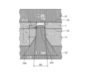
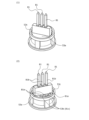
図1,3,4は、実施の形態にかかる半導体パッケージの製造途中(組立途中)の状態を示す断面図である。図2は、実施の形態にかかる半導体パッケージの製造途中(樹脂成形途中)の状態を示す断面図である。図1に示す実施の形態にかかる半導体パッケージ10は、半導体チップ(例えば後述する図5の圧力センサチップ61に相当)のハウジング部(例えば後述する図5のインナーハウジング部53に相当:樹脂成形品)に一体成形(インサート成形)された平板状の平板端子1(例えば後述する図5のコネクタピン81に相当)と、平板端子1の貫通孔(第1貫通孔)2を貫通する丸棒状の端子ピン21(例えば後述する図5のリードピン65に相当)と、を備える。
1a 平板端子の第1面
1b 平板端子の第2面
2 平板端子の貫通孔
2a 平板端子の貫通孔の第1部分
2b 平板端子の貫通孔の第2部分
10 半導体パッケージ
11 樹脂ガイド部
12 樹脂ガイド部の貫通孔
12a 樹脂ガイド部の貫通孔の第1部分
12b 樹脂ガイド部の貫通孔の第2部分
21 端子ピン
31 上部金型
32 下部金型
33 下部金型の突出部
33a 下部金型の突出部の第1部分
33b 下部金型の突出部の第2部分
33c 下部金型の突出部の第3部分
33d 下部金型の台座部
50 物理量センサ装置
51 センサエレメント
52 ネジ部(被測定媒体導入部)
53 インナーハウジング部
53a インナーハウジング部の上部
53b インナーハウジング部の上部の貫通孔
53c インナーハウジング部の上部の外周部の凹凸
53d インナーハウジング部の上部の溝
53e インナーハウジング部の凹部
54 ソケットハウジング部
54a ソケットハウジング部の下端部の凹凸
54b ソケットハウジング部の底部
54c ソケットハウジング部の底部の貫通孔
55 ソケットハウジング部に囲まれた空間
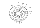
60 収納箱
60a 収納箱の凹部
60b 収納箱の貫通孔
60c 収納箱の注入孔
61 圧力センサチップ
62 台座部材
63 ダイアフラム
64 ボンディングワイヤ
65,65a,65b リードピン
66 絶縁性部材
70 液体
71 ネジ部の台座部
72 ネジ部の台座部と収納箱との溶接部
73 ネジ部の貫通孔
74 ネジ部の一方の開放端の圧力導入口(導入孔)
75 ネジ部の他方の開放端の開口部
76 オーリング
77 収納箱の凹み部
78,91 接着剤
81 コネクタピン
81a コネクタピンの水平部
81b コネクタピンの垂直部
81c コネクタピンの貫通孔
92 金属球
93 レーザー光
Claims (8)
- 平坦な両面を有する平板状の平板端子と、
前記平板端子の両面間を貫通する、前記平板端子に接合される棒状の端子ピンを貫通させるための第1貫通孔と、
樹脂を材料として前記平板端子の一方の面に一体成形されたガイド部と、
前記第1貫通孔と同じ中心軸を有し、前記ガイド部を貫通して前記第1貫通孔と連続する1つの孔をなす第2貫通孔と、
を備え、
前記孔は、前記第2貫通孔側の開放端から前記第1貫通孔側の開放端へ向かうにしたがって幅を狭くしたテーパー形状であり、
前記第2貫通孔の側壁と前記第1貫通孔の側壁とが同じ角度で連続する同一面であることを特徴とする樹脂成形品。 - 前記第2貫通孔の側壁の角度は、0°以上30°以下であることを特徴とする請求項1に記載の樹脂成形品。
- 前記第2貫通孔は、前記第1貫通孔から離れた部分で、前記第1貫通孔に連続する部分よりも側壁の角度が大きくなっていることを特徴とする請求項1または2に記載の樹脂成形品。
- 前記第1貫通孔は、前記第2貫通孔から離れた部分で、前記第2貫通孔に連続する部分よりも幅が狭く、かつ幅が一様であることを特徴とする請求項1~3のいずれか一つに記載の樹脂成形品。
- 請求項1~4のいずれか一つに記載の樹脂成形品を備えた半導体パッケージであって、
半導体チップと、
樹脂を材料として前記平板端子と一体成形された、前記半導体チップを収容する収容部と、
前記収容部の一部である前記ガイド部と、
前記第2貫通孔および前記第1貫通孔を貫通して前記平板端子の他方の面に露出する前記端子ピンと、
を備え、
前記端子ピンの一方の端部は、前記平板端子の他方の面で前記平板端子に接合され、
前記端子ピンの他方の端部は、前記半導体チップの電極に電気的に接続されていることを特徴とする半導体パッケージ。 - 前記端子ピンは、前記ガイド部から離れた部分で前記平板端子の前記第1貫通孔の側壁に接することを特徴とする請求項5に記載の半導体パッケージ。
- 平坦な両面を有する平板状の平板端子と、前記平板端子の両面間を貫通する、前記平板端子に接合される棒状の端子ピンを貫通させるための第1貫通孔と、前記平板端子の一方の面に一体成形されたガイド部と、前記第1貫通孔と同じ中心軸を有し、前記ガイド部を貫通して前記第1貫通孔と連続する1つの孔をなす第2貫通孔と、を備えた樹脂成形品の成形方法であって、
第1金型によって他方の面が支持された前記平板端子の一方の面と、第2金型と、の間に前記ガイド部の外形と同じ外形の空間を形成する第1工程と、
前記空間に樹脂を流し込んで充填して固化し、前記平板端子の一方の面に一体成形された前記ガイド部を形成する第2工程と、
を含み、
前記第2金型は、前記ガイド部の前記第2貫通孔を成形する箇所に、前記平板端子の一方の面側に突出し、かつ前記平板端子に近づくにしたがって幅を狭くしたテーパー形状の突出部を有し、
前記第1工程では、前記第2金型の前記突出部を前記平板端子の一方の面側から前記平板端子の前記第1貫通孔に挿入して前記第1貫通孔の開放端に圧接し、前記突出部で前記平板端子を支持するとともに、前記平板端子の前記第1貫通孔の、前記突出部で圧接した側壁の角度を前記突出部の側面と同じ角度にすることを特徴とする樹脂成形品の成形方法。 - 前記突出部の側面の角度は、0°以上30°以下であることを特徴とする請求項7に記載の樹脂成形品の成形方法。
Priority Applications (3)
| Application Number | Priority Date | Filing Date | Title |
|---|---|---|---|
| JP2020219109A JP7567472B2 (ja) | 2020-12-28 | 2020-12-28 | 半導体パッケージ、樹脂成形品および樹脂成形品の成形方法 |
| CN202111385892.8A CN114695128A (zh) | 2020-12-28 | 2021-11-22 | 半导体封装、树脂成型品及树脂成型品的成型方法 |
| US17/538,480 US12165938B2 (en) | 2020-12-28 | 2021-11-30 | Semiconductor package, resin molded product, and method of molding resin molded product |
Applications Claiming Priority (1)
| Application Number | Priority Date | Filing Date | Title |
|---|---|---|---|
| JP2020219109A JP7567472B2 (ja) | 2020-12-28 | 2020-12-28 | 半導体パッケージ、樹脂成形品および樹脂成形品の成形方法 |
Publications (2)
| Publication Number | Publication Date |
|---|---|
| JP2022104103A JP2022104103A (ja) | 2022-07-08 |
| JP7567472B2 true JP7567472B2 (ja) | 2024-10-16 |
Family
ID=82118458
Family Applications (1)
| Application Number | Title | Priority Date | Filing Date |
|---|---|---|---|
| JP2020219109A Active JP7567472B2 (ja) | 2020-12-28 | 2020-12-28 | 半導体パッケージ、樹脂成形品および樹脂成形品の成形方法 |
Country Status (3)
| Country | Link |
|---|---|
| US (1) | US12165938B2 (ja) |
| JP (1) | JP7567472B2 (ja) |
| CN (1) | CN114695128A (ja) |
Families Citing this family (1)
| Publication number | Priority date | Publication date | Assignee | Title |
|---|---|---|---|---|
| CN115799865A (zh) * | 2022-12-28 | 2023-03-14 | 昆山嘉华汽车电子科技有限公司 | 一种端子脚柔性卡接连接器 |
Citations (3)
| Publication number | Priority date | Publication date | Assignee | Title |
|---|---|---|---|---|
| WO2009087767A1 (ja) | 2008-01-10 | 2009-07-16 | Saginomiya Seisakusho, Inc. | 圧力センサ及びその製造方法 |
| US20180113042A1 (en) | 2015-04-16 | 2018-04-26 | Metallux Sa | Sensor for detecting one or more quantities of a fluid, in particular a pressure sensor |
| JP2018136277A (ja) | 2017-02-23 | 2018-08-30 | 富士電機株式会社 | 物理量センサ装置の製造方法および物理量センサ装置 |
Family Cites Families (5)
| Publication number | Priority date | Publication date | Assignee | Title |
|---|---|---|---|---|
| JP6139280B2 (ja) * | 2013-06-05 | 2017-05-31 | トヨタ自動車株式会社 | 半導体装置 |
| DE112017006813T5 (de) * | 2017-01-13 | 2019-10-02 | Mitsubishi Electric Corporation | Leistungshalbleitereinheit und verfahren zur herstellung einer leistungshalbleitereinheit |
| JP6809285B2 (ja) * | 2017-02-23 | 2021-01-06 | 富士電機株式会社 | 物理量センサ装置の製造方法および物理量センサ装置 |
| JP2020188113A (ja) * | 2019-05-14 | 2020-11-19 | 株式会社デンソー | 半導体装置 |
| JP7721910B2 (ja) * | 2021-02-17 | 2025-08-13 | 富士電機株式会社 | 物理量センサ装置および物理量センサ装置の製造方法 |
-
2020
- 2020-12-28 JP JP2020219109A patent/JP7567472B2/ja active Active
-
2021
- 2021-11-22 CN CN202111385892.8A patent/CN114695128A/zh active Pending
- 2021-11-30 US US17/538,480 patent/US12165938B2/en active Active
Patent Citations (3)
| Publication number | Priority date | Publication date | Assignee | Title |
|---|---|---|---|---|
| WO2009087767A1 (ja) | 2008-01-10 | 2009-07-16 | Saginomiya Seisakusho, Inc. | 圧力センサ及びその製造方法 |
| US20180113042A1 (en) | 2015-04-16 | 2018-04-26 | Metallux Sa | Sensor for detecting one or more quantities of a fluid, in particular a pressure sensor |
| JP2018136277A (ja) | 2017-02-23 | 2018-08-30 | 富士電機株式会社 | 物理量センサ装置の製造方法および物理量センサ装置 |
Also Published As
| Publication number | Publication date |
|---|---|
| JP2022104103A (ja) | 2022-07-08 |
| US12165938B2 (en) | 2024-12-10 |
| CN114695128A (zh) | 2022-07-01 |
| US20220208622A1 (en) | 2022-06-30 |
Similar Documents
| Publication | Publication Date | Title |
|---|---|---|
| JP3888228B2 (ja) | センサ装置 | |
| JP3165078B2 (ja) | 表面実装部品の製造方法 | |
| JP4830391B2 (ja) | センサ装置の製造方法及びセンサ装置 | |
| CN100433339C (zh) | 固体摄像器件及其制造方法 | |
| EP3124935B1 (en) | Sensor package | |
| CN105424260A (zh) | 压力传感器装置以及压力传感器装置的制造方法 | |
| JP6809285B2 (ja) | 物理量センサ装置の製造方法および物理量センサ装置 | |
| US7754130B2 (en) | Method for manufacturing physical quantity sensor | |
| JP4101033B2 (ja) | 圧力センサおよび圧力センサにおける端子接続方法 | |
| JP4908411B2 (ja) | 圧力センサ及びその製造方法 | |
| JP6809284B2 (ja) | 物理量センサ装置の製造方法および物理量センサ装置 | |
| JP7721910B2 (ja) | 物理量センサ装置および物理量センサ装置の製造方法 | |
| CN100433301C (zh) | 固态成像器件及其制造方法 | |
| JP2017037039A (ja) | 物理量センサ装置および物理量センサ装置の製造方法 | |
| KR20130138666A (ko) | 압력 센서 및 압력 센서의 제조 방법 | |
| CN114695128A (zh) | 半导体封装、树脂成型品及树脂成型品的成型方法 | |
| WO2009087767A1 (ja) | 圧力センサ及びその製造方法 | |
| JP5359344B2 (ja) | インサート樹脂成形部品の製造方法とそれに用いられる樹脂成形金型および圧力センサ | |
| JP2001118868A (ja) | 表面実装部品及びその製造方法 | |
| JP4742706B2 (ja) | 半導体装置及びその製造方法 | |
| JP3232486U (ja) | 物理量センサ装置 | |
| JP4049176B2 (ja) | 半導体装置及びその製造方法 | |
| JP4609476B2 (ja) | 半導体装置の封止樹脂層及び半導体装置の封止樹脂層の形成方法 | |
| JP2001237359A (ja) | 半導体装置 | |
| JP2006100312A (ja) | 光半導体装置および測距モジュール |
Legal Events
| Date | Code | Title | Description |
|---|---|---|---|
| A621 | Written request for application examination |
Free format text: JAPANESE INTERMEDIATE CODE: A621 Effective date: 20231113 |
|
| A977 | Report on retrieval |
Free format text: JAPANESE INTERMEDIATE CODE: A971007 Effective date: 20240731 |
|
| TRDD | Decision of grant or rejection written | ||
| A01 | Written decision to grant a patent or to grant a registration (utility model) |
Free format text: JAPANESE INTERMEDIATE CODE: A01 Effective date: 20240903 |
|
| A61 | First payment of annual fees (during grant procedure) |
Free format text: JAPANESE INTERMEDIATE CODE: A61 Effective date: 20240916 |
|
| R150 | Certificate of patent or registration of utility model |
Ref document number: 7567472 Country of ref document: JP Free format text: JAPANESE INTERMEDIATE CODE: R150 |