JP7585306B2 - 半導体装置 - Google Patents
半導体装置 Download PDFInfo
- Publication number
- JP7585306B2 JP7585306B2 JP2022511808A JP2022511808A JP7585306B2 JP 7585306 B2 JP7585306 B2 JP 7585306B2 JP 2022511808 A JP2022511808 A JP 2022511808A JP 2022511808 A JP2022511808 A JP 2022511808A JP 7585306 B2 JP7585306 B2 JP 7585306B2
- Authority
- JP
- Japan
- Prior art keywords
- semiconductor device
- metal film
- frame
- glass substrate
- wiring
- Prior art date
- Legal status (The legal status is an assumption and is not a legal conclusion. Google has not performed a legal analysis and makes no representation as to the accuracy of the status listed.)
- Active
Links
Images


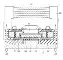


Classifications
-
- H—ELECTRICITY
- H10—SEMICONDUCTOR DEVICES; ELECTRIC SOLID-STATE DEVICES NOT OTHERWISE PROVIDED FOR
- H10W—GENERIC PACKAGES, INTERCONNECTIONS, CONNECTORS OR OTHER CONSTRUCTIONAL DETAILS OF DEVICES COVERED BY CLASS H10
- H10W70/00—Package substrates; Interposers; Redistribution layers [RDL]
- H10W70/60—Insulating or insulated package substrates; Interposers; Redistribution layers
- H10W70/67—Insulating or insulated package substrates; Interposers; Redistribution layers characterised by their insulating layers or insulating parts
- H10W70/69—Insulating materials thereof
- H10W70/692—Ceramics or glasses
-
- H—ELECTRICITY
- H01—ELECTRIC ELEMENTS
- H01Q—ANTENNAS, i.e. RADIO AERIALS
- H01Q1/00—Details of, or arrangements associated with, antennas
- H01Q1/12—Supports; Mounting means
- H01Q1/22—Supports; Mounting means by structural association with other equipment or articles
- H01Q1/2283—Supports; Mounting means by structural association with other equipment or articles mounted in or on the surface of a semiconductor substrate as a chip-type antenna or integrated with other components into an IC package
-
- H—ELECTRICITY
- H01—ELECTRIC ELEMENTS
- H01Q—ANTENNAS, i.e. RADIO AERIALS
- H01Q13/00—Waveguide horns or mouths; Slot antennas; Leaky-waveguide antennas; Equivalent structures causing radiation along the transmission path of a guided wave
- H01Q13/10—Resonant slot antennas
-
- H—ELECTRICITY
- H01—ELECTRIC ELEMENTS
- H01Q—ANTENNAS, i.e. RADIO AERIALS
- H01Q19/00—Combinations of primary active antenna elements and units with secondary devices, e.g. with quasi-optical devices, for giving the antenna a desired directional characteristic
- H01Q19/10—Combinations of primary active antenna elements and units with secondary devices, e.g. with quasi-optical devices, for giving the antenna a desired directional characteristic using reflecting surfaces
- H01Q19/12—Combinations of primary active antenna elements and units with secondary devices, e.g. with quasi-optical devices, for giving the antenna a desired directional characteristic using reflecting surfaces wherein the surfaces are concave
- H01Q19/13—Combinations of primary active antenna elements and units with secondary devices, e.g. with quasi-optical devices, for giving the antenna a desired directional characteristic using reflecting surfaces wherein the surfaces are concave the primary radiating source being a single radiating element, e.g. a dipole, a slot, a waveguide termination
-
- H—ELECTRICITY
- H01—ELECTRIC ELEMENTS
- H01Q—ANTENNAS, i.e. RADIO AERIALS
- H01Q19/00—Combinations of primary active antenna elements and units with secondary devices, e.g. with quasi-optical devices, for giving the antenna a desired directional characteristic
- H01Q19/28—Combinations of primary active antenna elements and units with secondary devices, e.g. with quasi-optical devices, for giving the antenna a desired directional characteristic using a secondary device in the form of two or more substantially straight conductive elements
- H01Q19/30—Combinations of primary active antenna elements and units with secondary devices, e.g. with quasi-optical devices, for giving the antenna a desired directional characteristic using a secondary device in the form of two or more substantially straight conductive elements the primary active element being centre-fed and substantially straight, e.g. Yagi antenna
-
- H—ELECTRICITY
- H01—ELECTRIC ELEMENTS
- H01Q—ANTENNAS, i.e. RADIO AERIALS
- H01Q21/00—Antenna arrays or systems
- H01Q21/06—Arrays of individually energised antenna units similarly polarised and spaced apart
- H01Q21/061—Two dimensional planar arrays
- H01Q21/064—Two dimensional planar arrays using horn or slot aerials
-
- H—ELECTRICITY
- H01—ELECTRIC ELEMENTS
- H01Q—ANTENNAS, i.e. RADIO AERIALS
- H01Q9/00—Electrically-short antennas having dimensions not more than twice the operating wavelength and consisting of conductive active radiating elements
- H01Q9/04—Resonant antennas
- H01Q9/06—Details
- H01Q9/065—Microstrip dipole antennas
-
- H—ELECTRICITY
- H10—SEMICONDUCTOR DEVICES; ELECTRIC SOLID-STATE DEVICES NOT OTHERWISE PROVIDED FOR
- H10D—INORGANIC ELECTRIC SEMICONDUCTOR DEVICES
- H10D84/00—Integrated devices formed in or on semiconductor substrates that comprise only semiconducting layers, e.g. on Si wafers or on GaAs-on-Si wafers
- H10D84/01—Manufacture or treatment
- H10D84/0123—Integrating together multiple components covered by H10D12/00 or H10D30/00, e.g. integrating multiple IGBTs
- H10D84/0126—Integrating together multiple components covered by H10D12/00 or H10D30/00, e.g. integrating multiple IGBTs the components including insulated gates, e.g. IGFETs
- H10D84/0165—Integrating together multiple components covered by H10D12/00 or H10D30/00, e.g. integrating multiple IGBTs the components including insulated gates, e.g. IGFETs the components including complementary IGFETs, e.g. CMOS devices
-
- H—ELECTRICITY
- H10—SEMICONDUCTOR DEVICES; ELECTRIC SOLID-STATE DEVICES NOT OTHERWISE PROVIDED FOR
- H10D—INORGANIC ELECTRIC SEMICONDUCTOR DEVICES
- H10D84/00—Integrated devices formed in or on semiconductor substrates that comprise only semiconducting layers, e.g. on Si wafers or on GaAs-on-Si wafers
- H10D84/01—Manufacture or treatment
- H10D84/02—Manufacture or treatment characterised by using material-based technologies
- H10D84/03—Manufacture or treatment characterised by using material-based technologies using Group IV technology, e.g. silicon technology or silicon-carbide [SiC] technology
- H10D84/038—Manufacture or treatment characterised by using material-based technologies using Group IV technology, e.g. silicon technology or silicon-carbide [SiC] technology using silicon technology, e.g. SiGe
-
- H—ELECTRICITY
- H10—SEMICONDUCTOR DEVICES; ELECTRIC SOLID-STATE DEVICES NOT OTHERWISE PROVIDED FOR
- H10F—INORGANIC SEMICONDUCTOR DEVICES SENSITIVE TO INFRARED RADIATION, LIGHT, ELECTROMAGNETIC RADIATION OF SHORTER WAVELENGTH OR CORPUSCULAR RADIATION
- H10F39/00—Integrated devices, or assemblies of multiple devices, comprising at least one element covered by group H10F30/00, e.g. radiation detectors comprising photodiode arrays
- H10F39/80—Constructional details of image sensors
- H10F39/804—Containers or encapsulations
-
- H—ELECTRICITY
- H10—SEMICONDUCTOR DEVICES; ELECTRIC SOLID-STATE DEVICES NOT OTHERWISE PROVIDED FOR
- H10W—GENERIC PACKAGES, INTERCONNECTIONS, CONNECTORS OR OTHER CONSTRUCTIONAL DETAILS OF DEVICES COVERED BY CLASS H10
- H10W20/00—Interconnections in chips, wafers or substrates
- H10W20/40—Interconnections external to wafers or substrates, e.g. back-end-of-line [BEOL] metallisations or vias connecting to gate electrodes
- H10W20/41—Interconnections external to wafers or substrates, e.g. back-end-of-line [BEOL] metallisations or vias connecting to gate electrodes characterised by their conductive parts
- H10W20/44—Conductive materials thereof
- H10W20/4403—Conductive materials thereof based on metals, e.g. alloys, metal silicides
- H10W20/4421—Conductive materials thereof based on metals, e.g. alloys, metal silicides the principal metal being copper
-
- H—ELECTRICITY
- H10—SEMICONDUCTOR DEVICES; ELECTRIC SOLID-STATE DEVICES NOT OTHERWISE PROVIDED FOR
- H10W—GENERIC PACKAGES, INTERCONNECTIONS, CONNECTORS OR OTHER CONSTRUCTIONAL DETAILS OF DEVICES COVERED BY CLASS H10
- H10W40/00—Arrangements for thermal protection or thermal control
- H10W40/60—Securing means for detachable heating or cooling arrangements, e.g. clamps
- H10W40/611—Bolts or screws
-
- H—ELECTRICITY
- H10—SEMICONDUCTOR DEVICES; ELECTRIC SOLID-STATE DEVICES NOT OTHERWISE PROVIDED FOR
- H10W—GENERIC PACKAGES, INTERCONNECTIONS, CONNECTORS OR OTHER CONSTRUCTIONAL DETAILS OF DEVICES COVERED BY CLASS H10
- H10W42/00—Arrangements for protection of devices
- H10W42/121—Arrangements for protection of devices protecting against mechanical damage
-
- H—ELECTRICITY
- H10—SEMICONDUCTOR DEVICES; ELECTRIC SOLID-STATE DEVICES NOT OTHERWISE PROVIDED FOR
- H10W—GENERIC PACKAGES, INTERCONNECTIONS, CONNECTORS OR OTHER CONSTRUCTIONAL DETAILS OF DEVICES COVERED BY CLASS H10
- H10W70/00—Package substrates; Interposers; Redistribution layers [RDL]
- H10W70/60—Insulating or insulated package substrates; Interposers; Redistribution layers
- H10W70/67—Insulating or insulated package substrates; Interposers; Redistribution layers characterised by their insulating layers or insulating parts
- H10W70/68—Shapes or dispositions thereof
-
- H—ELECTRICITY
- H10—SEMICONDUCTOR DEVICES; ELECTRIC SOLID-STATE DEVICES NOT OTHERWISE PROVIDED FOR
- H10W—GENERIC PACKAGES, INTERCONNECTIONS, CONNECTORS OR OTHER CONSTRUCTIONAL DETAILS OF DEVICES COVERED BY CLASS H10
- H10W76/00—Containers; Fillings or auxiliary members therefor; Seals
- H10W76/10—Containers or parts thereof
- H10W76/12—Containers or parts thereof characterised by their shape
-
- H—ELECTRICITY
- H10—SEMICONDUCTOR DEVICES; ELECTRIC SOLID-STATE DEVICES NOT OTHERWISE PROVIDED FOR
- H10W—GENERIC PACKAGES, INTERCONNECTIONS, CONNECTORS OR OTHER CONSTRUCTIONAL DETAILS OF DEVICES COVERED BY CLASS H10
- H10W76/00—Containers; Fillings or auxiliary members therefor; Seals
- H10W76/60—Seals
-
- H—ELECTRICITY
- H10—SEMICONDUCTOR DEVICES; ELECTRIC SOLID-STATE DEVICES NOT OTHERWISE PROVIDED FOR
- H10W—GENERIC PACKAGES, INTERCONNECTIONS, CONNECTORS OR OTHER CONSTRUCTIONAL DETAILS OF DEVICES COVERED BY CLASS H10
- H10W40/00—Arrangements for thermal protection or thermal control
- H10W40/20—Arrangements for cooling
- H10W40/22—Arrangements for cooling characterised by their shape, e.g. having conical or cylindrical projections
- H10W40/226—Arrangements for cooling characterised by their shape, e.g. having conical or cylindrical projections characterised by projecting parts, e.g. fins to increase surface area
- H10W40/228—Arrangements for cooling characterised by their shape, e.g. having conical or cylindrical projections characterised by projecting parts, e.g. fins to increase surface area the projecting parts being wire-shaped or pin-shaped
-
- H—ELECTRICITY
- H10—SEMICONDUCTOR DEVICES; ELECTRIC SOLID-STATE DEVICES NOT OTHERWISE PROVIDED FOR
- H10W—GENERIC PACKAGES, INTERCONNECTIONS, CONNECTORS OR OTHER CONSTRUCTIONAL DETAILS OF DEVICES COVERED BY CLASS H10
- H10W44/00—Electrical arrangements for controlling or matching impedance
- H10W44/20—Electrical arrangements for controlling or matching impedance at high-frequency [HF] or radio frequency [RF]
-
- H—ELECTRICITY
- H10—SEMICONDUCTOR DEVICES; ELECTRIC SOLID-STATE DEVICES NOT OTHERWISE PROVIDED FOR
- H10W—GENERIC PACKAGES, INTERCONNECTIONS, CONNECTORS OR OTHER CONSTRUCTIONAL DETAILS OF DEVICES COVERED BY CLASS H10
- H10W70/00—Package substrates; Interposers; Redistribution layers [RDL]
- H10W70/60—Insulating or insulated package substrates; Interposers; Redistribution layers
- H10W70/62—Insulating or insulated package substrates; Interposers; Redistribution layers characterised by their interconnections
- H10W70/63—Vias, e.g. via plugs
- H10W70/635—Through-vias
-
- H—ELECTRICITY
- H10—SEMICONDUCTOR DEVICES; ELECTRIC SOLID-STATE DEVICES NOT OTHERWISE PROVIDED FOR
- H10W—GENERIC PACKAGES, INTERCONNECTIONS, CONNECTORS OR OTHER CONSTRUCTIONAL DETAILS OF DEVICES COVERED BY CLASS H10
- H10W90/00—Package configurations
- H10W90/401—Package configurations characterised by multiple insulating or insulated package substrates, interposers or RDLs
Landscapes
- Engineering & Computer Science (AREA)
- Microelectronics & Electronic Packaging (AREA)
- Solid State Image Pick-Up Elements (AREA)
- Cooling Or The Like Of Semiconductors Or Solid State Devices (AREA)
- Chemical & Material Sciences (AREA)
- Ceramic Engineering (AREA)
Applications Claiming Priority (3)
| Application Number | Priority Date | Filing Date | Title |
|---|---|---|---|
| JP2020065040 | 2020-03-31 | ||
| JP2020065040 | 2020-03-31 | ||
| PCT/JP2021/010492 WO2021200094A1 (fr) | 2020-03-31 | 2021-03-16 | Dispositif à semi-conducteur |
Publications (2)
| Publication Number | Publication Date |
|---|---|
| JPWO2021200094A1 JPWO2021200094A1 (fr) | 2021-10-07 |
| JP7585306B2 true JP7585306B2 (ja) | 2024-11-18 |
Family
ID=77930359
Family Applications (1)
| Application Number | Title | Priority Date | Filing Date |
|---|---|---|---|
| JP2022511808A Active JP7585306B2 (ja) | 2020-03-31 | 2021-03-16 | 半導体装置 |
Country Status (5)
| Country | Link |
|---|---|
| US (1) | US12354923B2 (fr) |
| EP (1) | EP4131355B1 (fr) |
| JP (1) | JP7585306B2 (fr) |
| CN (1) | CN115315803A (fr) |
| WO (1) | WO2021200094A1 (fr) |
Families Citing this family (9)
| Publication number | Priority date | Publication date | Assignee | Title |
|---|---|---|---|---|
| US12228776B2 (en) | 2022-01-31 | 2025-02-18 | Taiwan Semiconductor Manufacturing Co., Ltd. | Package with integrated optical die and method forming same |
| WO2023243271A1 (fr) * | 2022-06-16 | 2023-12-21 | ソニーセミコンダクタソリューションズ株式会社 | Dispositif à semi-conducteur |
| US12616031B2 (en) | 2022-12-19 | 2026-04-28 | Avago Technologies International Sales Pte. Limited | Electromagnetic shielding structure |
| WO2025105035A1 (fr) * | 2023-11-13 | 2025-05-22 | ソニーセミコンダクタソリューションズ株式会社 | Boîtier de semi-conducteur, dispositif à semi-conducteur et procédé de fabrication de boîtier de semi-conducteur |
| US20250210586A1 (en) * | 2023-12-26 | 2025-06-26 | Intel Corporation | Semiconductor package substrate dicing and edge passivation |
| US20250374426A1 (en) * | 2024-06-03 | 2025-12-04 | Intel Corporation | Automated manufacturing of hybrid panels |
| US20240355749A1 (en) * | 2024-06-27 | 2024-10-24 | Intel Corporation | Disaggregated package substrates with glass cores |
| US20260005078A1 (en) * | 2024-06-27 | 2026-01-01 | Intel Corporation | Fabricating integrated circuit packages with glass core hybrid panels |
| US20260005160A1 (en) * | 2024-06-28 | 2026-01-01 | Intel Corporation | Hybrid panel with a glass substrate |
Citations (4)
| Publication number | Priority date | Publication date | Assignee | Title |
|---|---|---|---|---|
| JP2008235869A (ja) | 2007-01-23 | 2008-10-02 | Advanced Chip Engineering Technology Inc | イメージセンサモジュール構造および半導体デバイスパッケージの形成方法 |
| JP2015131741A (ja) | 2014-01-10 | 2015-07-23 | 株式会社Nsc | 端面保護層付きガラス基板の製造方法 |
| JP2015151286A (ja) | 2014-02-12 | 2015-08-24 | 大日本印刷株式会社 | カバーガラスの製造方法、カバーガラスおよびカバーガラス付き表示装置 |
| JP2016208057A (ja) | 2014-05-02 | 2016-12-08 | サムソン エレクトロ−メカニックス カンパニーリミテッド. | 印刷回路基板、印刷回路基板ストリップ及びその製造方法 |
Family Cites Families (6)
| Publication number | Priority date | Publication date | Assignee | Title |
|---|---|---|---|---|
| JPH0548231A (ja) * | 1991-08-09 | 1993-02-26 | Seiko Epson Corp | 密度の異なる回路基板の実装構造 |
| JP4660259B2 (ja) * | 2004-06-10 | 2011-03-30 | 三洋電機株式会社 | 半導体装置の製造方法 |
| JP6038517B2 (ja) * | 2012-07-13 | 2016-12-07 | 新光電気工業株式会社 | 配線基板及びその製造方法 |
| JP6331127B2 (ja) | 2014-03-28 | 2018-05-30 | 大日本印刷株式会社 | カバーガラスおよびカバーガラス付き表示装置 |
| US20190333850A1 (en) * | 2014-03-07 | 2019-10-31 | Bridge Semiconductor Corporation | Wiring board having bridging element straddling over interfaces |
| US10515929B2 (en) * | 2018-04-09 | 2019-12-24 | International Business Machines Corporation | Carrier and integrated memory |
-
2021
- 2021-03-16 JP JP2022511808A patent/JP7585306B2/ja active Active
- 2021-03-16 WO PCT/JP2021/010492 patent/WO2021200094A1/fr not_active Ceased
- 2021-03-16 EP EP21781042.3A patent/EP4131355B1/fr active Active
- 2021-03-16 US US17/906,873 patent/US12354923B2/en active Active
- 2021-03-16 CN CN202180023090.4A patent/CN115315803A/zh not_active Withdrawn
Patent Citations (4)
| Publication number | Priority date | Publication date | Assignee | Title |
|---|---|---|---|---|
| JP2008235869A (ja) | 2007-01-23 | 2008-10-02 | Advanced Chip Engineering Technology Inc | イメージセンサモジュール構造および半導体デバイスパッケージの形成方法 |
| JP2015131741A (ja) | 2014-01-10 | 2015-07-23 | 株式会社Nsc | 端面保護層付きガラス基板の製造方法 |
| JP2015151286A (ja) | 2014-02-12 | 2015-08-24 | 大日本印刷株式会社 | カバーガラスの製造方法、カバーガラスおよびカバーガラス付き表示装置 |
| JP2016208057A (ja) | 2014-05-02 | 2016-12-08 | サムソン エレクトロ−メカニックス カンパニーリミテッド. | 印刷回路基板、印刷回路基板ストリップ及びその製造方法 |
Also Published As
| Publication number | Publication date |
|---|---|
| US20230135956A1 (en) | 2023-05-04 |
| WO2021200094A1 (fr) | 2021-10-07 |
| EP4131355A4 (fr) | 2023-11-08 |
| JPWO2021200094A1 (fr) | 2021-10-07 |
| EP4131355A1 (fr) | 2023-02-08 |
| US12354923B2 (en) | 2025-07-08 |
| CN115315803A (zh) | 2022-11-08 |
| EP4131355B1 (fr) | 2024-10-23 |
Similar Documents
| Publication | Publication Date | Title |
|---|---|---|
| US12354923B2 (en) | Semiconductor device | |
| US12456669B2 (en) | Semiconductor device | |
| US20100321555A1 (en) | Solid state imaging device and manufacturing method thereof | |
| US20140240588A1 (en) | Electronic component and electronic apparatus | |
| US20180182801A1 (en) | Image sensor with processor package | |
| JP2012175273A (ja) | 撮像装置および撮像システム | |
| JP7491923B2 (ja) | シールドされた一体型デバイスパッケージ | |
| JP2004134710A (ja) | 半導体装置及びその製造方法、光モジュール及びその製造方法、回路基板並びに電子機器 | |
| US12160946B2 (en) | Image sensor package and camera device including same | |
| JP7406314B2 (ja) | 電子モジュール及び機器 | |
| US20240395643A1 (en) | Semiconductor device and electronic device | |
| WO2017141397A1 (fr) | Dispositif d'imagerie et endoscope | |
| JP2004274164A (ja) | 光モジュール及びその製造方法並びに電子機器 | |
| JP5045952B2 (ja) | 光デバイス、光モジュール及び電子機器 | |
| JP4292383B2 (ja) | 光デバイスの製造方法 | |
| WO2024181074A1 (fr) | Dispositif à semi-conducteur, appareil électronique et procédé de production de dispositif à semi-conducteur | |
| JP4145619B2 (ja) | 光モジュール及びその製造方法、回路基板並びに電子機器 | |
| WO2023135929A1 (fr) | Boîtier | |
| EP4542638A1 (fr) | Dispositif à semi-conducteur | |
| JP2004221876A (ja) | 光モジュール及びその製造方法並びに電子機器 | |
| JP4998689B2 (ja) | 光学機器モジュール | |
| JP2004282227A (ja) | 光モジュール及びその製造方法並びに電子機器 | |
| CN118763081A (zh) | 光子探测器及其制备方法 | |
| JP2014060689A (ja) | 撮像装置、該撮像装置を具備する内視鏡 |
Legal Events
| Date | Code | Title | Description |
|---|---|---|---|
| A621 | Written request for application examination |
Free format text: JAPANESE INTERMEDIATE CODE: A621 Effective date: 20240124 |
|
| TRDD | Decision of grant or rejection written | ||
| A01 | Written decision to grant a patent or to grant a registration (utility model) |
Free format text: JAPANESE INTERMEDIATE CODE: A01 Effective date: 20241008 |
|
| A61 | First payment of annual fees (during grant procedure) |
Free format text: JAPANESE INTERMEDIATE CODE: A61 Effective date: 20241106 |
|
| R150 | Certificate of patent or registration of utility model |
Ref document number: 7585306 Country of ref document: JP Free format text: JAPANESE INTERMEDIATE CODE: R150 |