JP7600848B2 - 半導体装置 - Google Patents
半導体装置 Download PDFInfo
- Publication number
- JP7600848B2 JP7600848B2 JP2021075293A JP2021075293A JP7600848B2 JP 7600848 B2 JP7600848 B2 JP 7600848B2 JP 2021075293 A JP2021075293 A JP 2021075293A JP 2021075293 A JP2021075293 A JP 2021075293A JP 7600848 B2 JP7600848 B2 JP 7600848B2
- Authority
- JP
- Japan
- Prior art keywords
- region
- range
- type
- diode
- contact
- Prior art date
- Legal status (The legal status is an assumption and is not a legal conclusion. Google has not performed a legal analysis and makes no representation as to the accuracy of the status listed.)
- Active
Links
Images



Classifications
-
- H—ELECTRICITY
- H10—SEMICONDUCTOR DEVICES; ELECTRIC SOLID-STATE DEVICES NOT OTHERWISE PROVIDED FOR
- H10D—INORGANIC ELECTRIC SEMICONDUCTOR DEVICES
- H10D8/00—Diodes
-
- H—ELECTRICITY
- H10—SEMICONDUCTOR DEVICES; ELECTRIC SOLID-STATE DEVICES NOT OTHERWISE PROVIDED FOR
- H10D—INORGANIC ELECTRIC SEMICONDUCTOR DEVICES
- H10D84/00—Integrated devices formed in or on semiconductor substrates that comprise only semiconducting layers, e.g. on Si wafers or on GaAs-on-Si wafers
- H10D84/60—Integrated devices formed in or on semiconductor substrates that comprise only semiconducting layers, e.g. on Si wafers or on GaAs-on-Si wafers characterised by the integration of at least one component covered by groups H10D10/00 or H10D18/00, e.g. integration of BJTs
- H10D84/611—Combinations of BJTs and one or more of diodes, resistors or capacitors
- H10D84/613—Combinations of vertical BJTs and one or more of diodes, resistors or capacitors
- H10D84/617—Combinations of vertical BJTs and only diodes
-
- H—ELECTRICITY
- H10—SEMICONDUCTOR DEVICES; ELECTRIC SOLID-STATE DEVICES NOT OTHERWISE PROVIDED FOR
- H10D—INORGANIC ELECTRIC SEMICONDUCTOR DEVICES
- H10D12/00—Bipolar devices controlled by the field effect, e.g. insulated-gate bipolar transistors [IGBT]
- H10D12/411—Insulated-gate bipolar transistors [IGBT]
- H10D12/441—Vertical IGBTs
- H10D12/461—Vertical IGBTs having non-planar surfaces, e.g. having trenches, recesses or pillars in the surfaces of the emitter, base or collector regions
- H10D12/481—Vertical IGBTs having non-planar surfaces, e.g. having trenches, recesses or pillars in the surfaces of the emitter, base or collector regions having gate structures on slanted surfaces, on vertical surfaces, or in grooves, e.g. trench gate IGBTs
-
- H—ELECTRICITY
- H10—SEMICONDUCTOR DEVICES; ELECTRIC SOLID-STATE DEVICES NOT OTHERWISE PROVIDED FOR
- H10D—INORGANIC ELECTRIC SEMICONDUCTOR DEVICES
- H10D30/00—Field-effect transistors [FET]
- H10D30/60—Insulated-gate field-effect transistors [IGFET]
-
- H—ELECTRICITY
- H10—SEMICONDUCTOR DEVICES; ELECTRIC SOLID-STATE DEVICES NOT OTHERWISE PROVIDED FOR
- H10D—INORGANIC ELECTRIC SEMICONDUCTOR DEVICES
- H10D62/00—Semiconductor bodies, or regions thereof, of devices having potential barriers
- H10D62/10—Shapes, relative sizes or dispositions of the regions of the semiconductor bodies; Shapes of the semiconductor bodies
- H10D62/102—Constructional design considerations for preventing surface leakage or controlling electric field concentration
- H10D62/103—Constructional design considerations for preventing surface leakage or controlling electric field concentration for increasing or controlling the breakdown voltage of reverse-biased devices
- H10D62/105—Constructional design considerations for preventing surface leakage or controlling electric field concentration for increasing or controlling the breakdown voltage of reverse-biased devices by having particular doping profiles, shapes or arrangements of PN junctions; by having supplementary regions, e.g. junction termination extension [JTE]
- H10D62/106—Constructional design considerations for preventing surface leakage or controlling electric field concentration for increasing or controlling the breakdown voltage of reverse-biased devices by having particular doping profiles, shapes or arrangements of PN junctions; by having supplementary regions, e.g. junction termination extension [JTE] having supplementary regions doped oppositely to or in rectifying contact with regions of the semiconductor bodies, e.g. guard rings with PN or Schottky junctions
- H10D62/107—Buried supplementary regions, e.g. buried guard rings
-
- H—ELECTRICITY
- H10—SEMICONDUCTOR DEVICES; ELECTRIC SOLID-STATE DEVICES NOT OTHERWISE PROVIDED FOR
- H10D—INORGANIC ELECTRIC SEMICONDUCTOR DEVICES
- H10D62/00—Semiconductor bodies, or regions thereof, of devices having potential barriers
- H10D62/10—Shapes, relative sizes or dispositions of the regions of the semiconductor bodies; Shapes of the semiconductor bodies
- H10D62/102—Constructional design considerations for preventing surface leakage or controlling electric field concentration
- H10D62/112—Constructional design considerations for preventing surface leakage or controlling electric field concentration for preventing surface leakage due to surface inversion layers, e.g. by using channel stoppers
-
- H—ELECTRICITY
- H10—SEMICONDUCTOR DEVICES; ELECTRIC SOLID-STATE DEVICES NOT OTHERWISE PROVIDED FOR
- H10D—INORGANIC ELECTRIC SEMICONDUCTOR DEVICES
- H10D62/00—Semiconductor bodies, or regions thereof, of devices having potential barriers
- H10D62/10—Shapes, relative sizes or dispositions of the regions of the semiconductor bodies; Shapes of the semiconductor bodies
- H10D62/17—Semiconductor regions connected to electrodes not carrying current to be rectified, amplified or switched, e.g. channel regions
- H10D62/393—Body regions of DMOS transistors or IGBTs
-
- H—ELECTRICITY
- H10—SEMICONDUCTOR DEVICES; ELECTRIC SOLID-STATE DEVICES NOT OTHERWISE PROVIDED FOR
- H10D—INORGANIC ELECTRIC SEMICONDUCTOR DEVICES
- H10D8/00—Diodes
- H10D8/422—PN diodes having the PN junctions in mesas
-
- H—ELECTRICITY
- H10—SEMICONDUCTOR DEVICES; ELECTRIC SOLID-STATE DEVICES NOT OTHERWISE PROVIDED FOR
- H10D—INORGANIC ELECTRIC SEMICONDUCTOR DEVICES
- H10D84/00—Integrated devices formed in or on semiconductor substrates that comprise only semiconducting layers, e.g. on Si wafers or on GaAs-on-Si wafers
- H10D84/80—Integrated devices formed in or on semiconductor substrates that comprise only semiconducting layers, e.g. on Si wafers or on GaAs-on-Si wafers characterised by the integration of at least one component covered by groups H10D12/00 or H10D30/00, e.g. integration of IGFETs
- H10D84/811—Combinations of field-effect devices and one or more diodes, capacitors or resistors
-
- H—ELECTRICITY
- H10—SEMICONDUCTOR DEVICES; ELECTRIC SOLID-STATE DEVICES NOT OTHERWISE PROVIDED FOR
- H10W—GENERIC PACKAGES, INTERCONNECTIONS, CONNECTORS OR OTHER CONSTRUCTIONAL DETAILS OF DEVICES COVERED BY CLASS H10
- H10W10/00—Isolation regions in semiconductor bodies between components of integrated devices
-
- H—ELECTRICITY
- H10—SEMICONDUCTOR DEVICES; ELECTRIC SOLID-STATE DEVICES NOT OTHERWISE PROVIDED FOR
- H10W—GENERIC PACKAGES, INTERCONNECTIONS, CONNECTORS OR OTHER CONSTRUCTIONAL DETAILS OF DEVICES COVERED BY CLASS H10
- H10W10/00—Isolation regions in semiconductor bodies between components of integrated devices
- H10W10/01—Manufacture or treatment
-
- H—ELECTRICITY
- H10—SEMICONDUCTOR DEVICES; ELECTRIC SOLID-STATE DEVICES NOT OTHERWISE PROVIDED FOR
- H10D—INORGANIC ELECTRIC SEMICONDUCTOR DEVICES
- H10D12/00—Bipolar devices controlled by the field effect, e.g. insulated-gate bipolar transistors [IGBT]
- H10D12/211—Gated diodes
Landscapes
- Metal-Oxide And Bipolar Metal-Oxide Semiconductor Integrated Circuits (AREA)
- Semiconductor Integrated Circuits (AREA)
Description
図6に示す参考例1の半導体装置では、IGBT範囲30内の表層金属層16bうちのダイオード範囲50に隣接する部分16b-2が、その他の部分16b-1よりも抵抗率が高い金属により構成されている。より詳細には、部分16b-1がアルミニウムにより構成されており、部分16b-2がアルミニウムよりも抵抗率が高い金属により構成されている。したがって、ダイオードがオンしているときに、図6の矢印102に示す経路(すなわち、IGBT範囲30とダイオード範囲50の境界)にホールが流れることが抑制される。したがって、ダイオードの逆回復動作において、IGBT範囲30とダイオード範囲50の境界に逆回復電流が流れることが抑制される。したがって、逆回復損失Errを抑制することができる。
図7に示す参考例2の半導体装置では、バッファ領域34が、高濃度領域34aと低濃度領域34bを有している。低濃度領域34bのn型不純物濃度は、高濃度領域34aのn型不純物濃度よりも低い。低濃度領域34bは、ダイオード範囲50内であって、コレクタ領域32とカソード領域52の境界60に隣接する位置に配置されている。高濃度領域34aは、IGBT範囲30内のバッファ領域34の全体と、ダイオード範囲50内のバッファ領域34の境界60近傍以外の部分を構成している。低濃度領域34bのn型不純物濃度が高濃度領域34aのn型不純物濃度よりも低いので、低濃度領域34bの抵抗率は高濃度領域34aの抵抗率よりも低い。したがって、ダイオードがオンしているときに、図7の矢印102に示す経路(すなわち、IGBT範囲30とダイオード範囲50の境界)にホールが流れることが抑制される。したがって、ダイオードの逆回復動作において、IGBT範囲30とダイオード範囲50の境界に逆回復電流が流れることが抑制される。したがって、逆回復損失Errを抑制することができる。
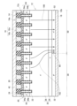
図8に示す参考例3の半導体装置では、IGBT範囲30内のうちのIGBT範囲30とダイオード範囲50の境界に隣接する範囲30xにおいて、その他の範囲よりもトレンチ20の間の間隔が狭い。このため、範囲30x内において、トレンチ20に挟まれた部分のボディ領域44の幅が狭い。このため、ダイオードがオンしているときに、範囲30x内のボディ領域44からドリフト領域36にホールが流入し難い。また、範囲30x内においてコンタクトホール14aの幅が細いことによっても、範囲30x内のボディ領域44からドリフト領域36にホールが流入することが抑制される。したがって、ダイオードがオンしているときに、図8の矢印102に示す経路(すなわち、IGBT範囲30とダイオード範囲50の境界)にホールが流れることが抑制される。したがって、ダイオードの逆回復動作において、IGBT範囲30とダイオード範囲50の境界に逆回復電流が流れることが抑制される。したがって、逆回復損失Errを抑制することができる。
12:半導体基板
14:層間絶縁膜
16:上部電極
18:下部電極
20:トレンチ
22:ゲート絶縁膜
24:ゲート電極
30:IGBT範囲
32:コレクタ領域
34:バッファ領域
36:ドリフト領域
38:電流制限領域
42:エミッタ領域
44:ボディ領域
50:ダイオード範囲
52:カソード領域
54:アノード領域
60:境界
Claims (4)
- 半導体装置であって、
半導体基板と、
前記半導体基板の下面に接する下部電極と、
ゲート絶縁膜と、
ゲート電極、
を有し、
前記半導体基板が、
前記下部電極に接するp型のコレクタ領域と、
前記コレクタ領域に隣接する位置で前記下部電極に接するn型のカソード領域、
を有し、
前記半導体基板が、
前記半導体基板の厚み方向に沿って見たときに前記コレクタ領域と重複する絶縁ゲートバイポーラトランジスタ範囲と、
前記半導体基板の厚み方向に沿って見たときに前記カソード領域と重複するダイオード範囲、
を有し、
前記半導体基板が、
前記絶縁ゲートバイポーラトランジスタ範囲と前記ダイオード範囲に跨って分布しており、前記コレクタ領域の上面と前記カソード領域の上面に接しており、前記カソード領域よりもn型不純物濃度が低いn型のバッファ領域と、
前記絶縁ゲートバイポーラトランジスタ範囲と前記ダイオード範囲に跨って分布しており、前記バッファ領域の上面に接しており、前記バッファ領域よりもn型不純物濃度が低いn型のドリフト領域と、
前記絶縁ゲートバイポーラトランジスタ範囲内に配置されており、前記ドリフト領域に接しているp型のボディ領域と、
前記絶縁ゲートバイポーラトランジスタ範囲内に配置されており、前記ボディ領域によって前記ドリフト領域から分離されているn型のソース領域と、
前記ダイオード範囲内に配置されており、前記ドリフト領域に接しているp型のアノード領域と、
前記コレクタ領域と前記カソード領域の境界の上部に配置されており、前記バッファ領域の上面に接しており、前記ドリフト領域に接しており、前記バッファ領域と前記ドリフト領域によって構成されるn型領域内でフローティングしているp型の電流制限領域、
を有し、
前記ゲート電極が、前記ゲート絶縁膜を介して前記ボディ領域に対向している、
半導体装置。 - 前記電流制限領域の側面に前記ドリフト領域が接している、請求項1に記載の半導体装置。
- 前記バッファ領域と前記ドリフト領域によって構成される前記n型領域内でフローティングしているp型の領域が、前記電流制限領域以外に存在しない、請求項1または2に記載の半導体装置。
- 前記コレクタ領域と前記カソード領域の前記境界から前記カソード領域の上部の前記電流制限領域の側面までの前記半導体基板の前記下面に沿う方向における距離が20μm以上である、請求項1~3のいずれか一項に記載の半導体装置。
Priority Applications (4)
| Application Number | Priority Date | Filing Date | Title |
|---|---|---|---|
| JP2021075293A JP7600848B2 (ja) | 2021-04-27 | 2021-04-27 | 半導体装置 |
| CN202180097436.5A CN117203777A (zh) | 2021-04-27 | 2021-10-08 | 半导体装置 |
| PCT/JP2021/037476 WO2022230216A1 (ja) | 2021-04-27 | 2021-10-08 | 半導体装置 |
| US18/464,312 US20230420453A1 (en) | 2021-04-27 | 2023-09-11 | Semiconductor device |
Applications Claiming Priority (1)
| Application Number | Priority Date | Filing Date | Title |
|---|---|---|---|
| JP2021075293A JP7600848B2 (ja) | 2021-04-27 | 2021-04-27 | 半導体装置 |
Publications (2)
| Publication Number | Publication Date |
|---|---|
| JP2022169322A JP2022169322A (ja) | 2022-11-09 |
| JP7600848B2 true JP7600848B2 (ja) | 2024-12-17 |
Family
ID=83846851
Family Applications (1)
| Application Number | Title | Priority Date | Filing Date |
|---|---|---|---|
| JP2021075293A Active JP7600848B2 (ja) | 2021-04-27 | 2021-04-27 | 半導体装置 |
Country Status (4)
| Country | Link |
|---|---|
| US (1) | US20230420453A1 (ja) |
| JP (1) | JP7600848B2 (ja) |
| CN (1) | CN117203777A (ja) |
| WO (1) | WO2022230216A1 (ja) |
Families Citing this family (5)
| Publication number | Priority date | Publication date | Assignee | Title |
|---|---|---|---|---|
| JP7717010B2 (ja) * | 2022-03-08 | 2025-08-01 | 株式会社デンソー | 半導体装置 |
| CN115985969A (zh) * | 2023-02-16 | 2023-04-18 | 青岛佳恩半导体有限公司 | 一种快恢复二极管芯片及其制造方法 |
| JP2024148755A (ja) * | 2023-04-06 | 2024-10-18 | ミネベアパワーデバイス株式会社 | 半導体装置 |
| JP2024151483A (ja) * | 2023-04-12 | 2024-10-25 | ミネベアパワーデバイス株式会社 | 半導体装置 |
| JP2024154946A (ja) * | 2023-04-20 | 2024-10-31 | ミネベアパワーデバイス株式会社 | 半導体装置 |
Citations (8)
| Publication number | Priority date | Publication date | Assignee | Title |
|---|---|---|---|---|
| JP2002343967A (ja) | 2001-05-14 | 2002-11-29 | Toyota Central Res & Dev Lab Inc | 半導体装置 |
| JP2004146679A (ja) | 2002-10-25 | 2004-05-20 | Toyota Central Res & Dev Lab Inc | バイポーラ型半導体装置とその製造方法 |
| JP2015177057A (ja) | 2014-03-14 | 2015-10-05 | 株式会社東芝 | 半導体装置 |
| WO2017146148A1 (ja) | 2016-02-23 | 2017-08-31 | 富士電機株式会社 | 半導体装置 |
| WO2018034127A1 (ja) | 2016-08-19 | 2018-02-22 | ローム株式会社 | 半導体装置 |
| WO2018220879A1 (ja) | 2017-05-31 | 2018-12-06 | 富士電機株式会社 | 半導体装置 |
| WO2019013286A1 (ja) | 2017-07-14 | 2019-01-17 | 富士電機株式会社 | 半導体装置 |
| JP2019125597A (ja) | 2018-01-11 | 2019-07-25 | トヨタ自動車株式会社 | 半導体装置 |
Family Cites Families (1)
| Publication number | Priority date | Publication date | Assignee | Title |
|---|---|---|---|---|
| JP7024626B2 (ja) * | 2018-06-27 | 2022-02-24 | 三菱電機株式会社 | 半導体装置、半導体装置の製造方法 |
-
2021
- 2021-04-27 JP JP2021075293A patent/JP7600848B2/ja active Active
- 2021-10-08 WO PCT/JP2021/037476 patent/WO2022230216A1/ja not_active Ceased
- 2021-10-08 CN CN202180097436.5A patent/CN117203777A/zh active Pending
-
2023
- 2023-09-11 US US18/464,312 patent/US20230420453A1/en active Pending
Patent Citations (8)
| Publication number | Priority date | Publication date | Assignee | Title |
|---|---|---|---|---|
| JP2002343967A (ja) | 2001-05-14 | 2002-11-29 | Toyota Central Res & Dev Lab Inc | 半導体装置 |
| JP2004146679A (ja) | 2002-10-25 | 2004-05-20 | Toyota Central Res & Dev Lab Inc | バイポーラ型半導体装置とその製造方法 |
| JP2015177057A (ja) | 2014-03-14 | 2015-10-05 | 株式会社東芝 | 半導体装置 |
| WO2017146148A1 (ja) | 2016-02-23 | 2017-08-31 | 富士電機株式会社 | 半導体装置 |
| WO2018034127A1 (ja) | 2016-08-19 | 2018-02-22 | ローム株式会社 | 半導体装置 |
| WO2018220879A1 (ja) | 2017-05-31 | 2018-12-06 | 富士電機株式会社 | 半導体装置 |
| WO2019013286A1 (ja) | 2017-07-14 | 2019-01-17 | 富士電機株式会社 | 半導体装置 |
| JP2019125597A (ja) | 2018-01-11 | 2019-07-25 | トヨタ自動車株式会社 | 半導体装置 |
Also Published As
| Publication number | Publication date |
|---|---|
| US20230420453A1 (en) | 2023-12-28 |
| JP2022169322A (ja) | 2022-11-09 |
| WO2022230216A1 (ja) | 2022-11-03 |
| CN117203777A (zh) | 2023-12-08 |
Similar Documents
| Publication | Publication Date | Title |
|---|---|---|
| JP7600848B2 (ja) | 半導体装置 | |
| US9960165B2 (en) | Semiconductor device having adjacent IGBT and diode regions with a shifted boundary plane between a collector region and a cathode region | |
| JP6053050B2 (ja) | 逆導通igbt | |
| US20100224907A1 (en) | Semiconductor device | |
| US10700054B2 (en) | Semiconductor apparatus | |
| JP6606007B2 (ja) | スイッチング素子 | |
| WO2016009714A1 (ja) | 半導体装置 | |
| CN110034184B (zh) | 半导体装置 | |
| US12363929B2 (en) | Semiconductor device | |
| US20230369484A1 (en) | Field effect transistor | |
| JP5324157B2 (ja) | 半導体装置およびその製造方法 | |
| JP2019161112A (ja) | 半導体装置 | |
| WO2024029153A1 (ja) | 絶縁ゲート型バイポーラトランジスタ | |
| WO2024042814A1 (ja) | 電界効果トランジスタ | |
| CN110246840A (zh) | 半导体装置 | |
| JP7352151B2 (ja) | スイッチング素子 | |
| JP2024072452A (ja) | 半導体装置 | |
| JP2006295062A (ja) | 半導体装置 | |
| US20260129956A1 (en) | Field-effect transistor | |
| CN121773720A (zh) | 半导体元件 | |
| JP2025021163A (ja) | 電界効果トランジスタ | |
| JP2024130276A (ja) | 半導体装置 | |
| WO2026048875A1 (ja) | 半導体装置 | |
| WO2026048876A1 (ja) | 半導体装置 | |
| JP5114865B2 (ja) | 半導体装置 |
Legal Events
| Date | Code | Title | Description |
|---|---|---|---|
| A621 | Written request for application examination |
Free format text: JAPANESE INTERMEDIATE CODE: A621 Effective date: 20230417 |
|
| A131 | Notification of reasons for refusal |
Free format text: JAPANESE INTERMEDIATE CODE: A131 Effective date: 20240702 |
|
| TRDD | Decision of grant or rejection written | ||
| A01 | Written decision to grant a patent or to grant a registration (utility model) |
Free format text: JAPANESE INTERMEDIATE CODE: A01 Effective date: 20241105 |
|
| A61 | First payment of annual fees (during grant procedure) |
Free format text: JAPANESE INTERMEDIATE CODE: A61 Effective date: 20241118 |
|
| R150 | Certificate of patent or registration of utility model |
Ref document number: 7600848 Country of ref document: JP Free format text: JAPANESE INTERMEDIATE CODE: R150 |