JP7601240B2 - 炭化珪素半導体装置および炭化珪素半導体基板 - Google Patents
炭化珪素半導体装置および炭化珪素半導体基板 Download PDFInfo
- Publication number
- JP7601240B2 JP7601240B2 JP2023545122A JP2023545122A JP7601240B2 JP 7601240 B2 JP7601240 B2 JP 7601240B2 JP 2023545122 A JP2023545122 A JP 2023545122A JP 2023545122 A JP2023545122 A JP 2023545122A JP 7601240 B2 JP7601240 B2 JP 7601240B2
- Authority
- JP
- Japan
- Prior art keywords
- impurity concentration
- region
- semiconductor region
- type
- silicon carbide
- Prior art date
- Legal status (The legal status is an assumption and is not a legal conclusion. Google has not performed a legal analysis and makes no representation as to the accuracy of the status listed.)
- Active
Links
Images

Classifications
-
- H—ELECTRICITY
- H10—SEMICONDUCTOR DEVICES; ELECTRIC SOLID-STATE DEVICES NOT OTHERWISE PROVIDED FOR
- H10D—INORGANIC ELECTRIC SEMICONDUCTOR DEVICES
- H10D84/00—Integrated devices formed in or on semiconductor substrates that comprise only semiconducting layers, e.g. on Si wafers or on GaAs-on-Si wafers
- H10D84/101—Integrated devices comprising main components and built-in components, e.g. IGBT having built-in freewheel diode
- H10D84/141—VDMOS having built-in components
- H10D84/143—VDMOS having built-in components the built-in components being PN junction diodes
- H10D84/144—VDMOS having built-in components the built-in components being PN junction diodes in antiparallel diode configurations
-
- H—ELECTRICITY
- H10—SEMICONDUCTOR DEVICES; ELECTRIC SOLID-STATE DEVICES NOT OTHERWISE PROVIDED FOR
- H10D—INORGANIC ELECTRIC SEMICONDUCTOR DEVICES
- H10D12/00—Bipolar devices controlled by the field effect, e.g. insulated-gate bipolar transistors [IGBT]
-
- H—ELECTRICITY
- H10—SEMICONDUCTOR DEVICES; ELECTRIC SOLID-STATE DEVICES NOT OTHERWISE PROVIDED FOR
- H10D—INORGANIC ELECTRIC SEMICONDUCTOR DEVICES
- H10D30/00—Field-effect transistors [FET]
- H10D30/01—Manufacture or treatment
- H10D30/021—Manufacture or treatment of FETs having insulated gates [IGFET]
-
- H—ELECTRICITY
- H10—SEMICONDUCTOR DEVICES; ELECTRIC SOLID-STATE DEVICES NOT OTHERWISE PROVIDED FOR
- H10D—INORGANIC ELECTRIC SEMICONDUCTOR DEVICES
- H10D30/00—Field-effect transistors [FET]
- H10D30/60—Insulated-gate field-effect transistors [IGFET]
-
- H—ELECTRICITY
- H10—SEMICONDUCTOR DEVICES; ELECTRIC SOLID-STATE DEVICES NOT OTHERWISE PROVIDED FOR
- H10D—INORGANIC ELECTRIC SEMICONDUCTOR DEVICES
- H10D30/00—Field-effect transistors [FET]
- H10D30/60—Insulated-gate field-effect transistors [IGFET]
- H10D30/64—Double-diffused metal-oxide semiconductor [DMOS] FETs
- H10D30/66—Vertical DMOS [VDMOS] FETs
- H10D30/668—Vertical DMOS [VDMOS] FETs having trench gate electrodes, e.g. UMOS transistors
-
- H—ELECTRICITY
- H10—SEMICONDUCTOR DEVICES; ELECTRIC SOLID-STATE DEVICES NOT OTHERWISE PROVIDED FOR
- H10D—INORGANIC ELECTRIC SEMICONDUCTOR DEVICES
- H10D62/00—Semiconductor bodies, or regions thereof, of devices having potential barriers
- H10D62/10—Shapes, relative sizes or dispositions of the regions of the semiconductor bodies; Shapes of the semiconductor bodies
- H10D62/102—Constructional design considerations for preventing surface leakage or controlling electric field concentration
- H10D62/103—Constructional design considerations for preventing surface leakage or controlling electric field concentration for increasing or controlling the breakdown voltage of reverse-biased devices
- H10D62/105—Constructional design considerations for preventing surface leakage or controlling electric field concentration for increasing or controlling the breakdown voltage of reverse-biased devices by having particular doping profiles, shapes or arrangements of PN junctions; by having supplementary regions, e.g. junction termination extension [JTE]
- H10D62/106—Constructional design considerations for preventing surface leakage or controlling electric field concentration for increasing or controlling the breakdown voltage of reverse-biased devices by having particular doping profiles, shapes or arrangements of PN junctions; by having supplementary regions, e.g. junction termination extension [JTE] having supplementary regions doped oppositely to or in rectifying contact with regions of the semiconductor bodies, e.g. guard rings with PN or Schottky junctions
- H10D62/107—Buried supplementary regions, e.g. buried guard rings
-
- H—ELECTRICITY
- H10—SEMICONDUCTOR DEVICES; ELECTRIC SOLID-STATE DEVICES NOT OTHERWISE PROVIDED FOR
- H10D—INORGANIC ELECTRIC SEMICONDUCTOR DEVICES
- H10D62/00—Semiconductor bodies, or regions thereof, of devices having potential barriers
- H10D62/10—Shapes, relative sizes or dispositions of the regions of the semiconductor bodies; Shapes of the semiconductor bodies
- H10D62/13—Semiconductor regions connected to electrodes carrying current to be rectified, amplified or switched, e.g. source or drain regions
- H10D62/149—Source or drain regions of field-effect devices
- H10D62/151—Source or drain regions of field-effect devices of IGFETs
- H10D62/156—Drain regions of DMOS transistors
- H10D62/157—Impurity concentrations or distributions
-
- H—ELECTRICITY
- H10—SEMICONDUCTOR DEVICES; ELECTRIC SOLID-STATE DEVICES NOT OTHERWISE PROVIDED FOR
- H10D—INORGANIC ELECTRIC SEMICONDUCTOR DEVICES
- H10D62/00—Semiconductor bodies, or regions thereof, of devices having potential barriers
- H10D62/10—Shapes, relative sizes or dispositions of the regions of the semiconductor bodies; Shapes of the semiconductor bodies
- H10D62/17—Semiconductor regions connected to electrodes not carrying current to be rectified, amplified or switched, e.g. channel regions
- H10D62/393—Body regions of DMOS transistors or IGBTs
-
- H—ELECTRICITY
- H10—SEMICONDUCTOR DEVICES; ELECTRIC SOLID-STATE DEVICES NOT OTHERWISE PROVIDED FOR
- H10D—INORGANIC ELECTRIC SEMICONDUCTOR DEVICES
- H10D62/00—Semiconductor bodies, or regions thereof, of devices having potential barriers
- H10D62/80—Semiconductor bodies, or regions thereof, of devices having potential barriers characterised by the materials
- H10D62/83—Semiconductor bodies, or regions thereof, of devices having potential barriers characterised by the materials being Group IV materials, e.g. B-doped Si or undoped Ge
- H10D62/832—Semiconductor bodies, or regions thereof, of devices having potential barriers characterised by the materials being Group IV materials, e.g. B-doped Si or undoped Ge being Group IV materials comprising two or more elements, e.g. SiGe
- H10D62/8325—Silicon carbide
-
- H—ELECTRICITY
- H10—SEMICONDUCTOR DEVICES; ELECTRIC SOLID-STATE DEVICES NOT OTHERWISE PROVIDED FOR
- H10D—INORGANIC ELECTRIC SEMICONDUCTOR DEVICES
- H10D12/00—Bipolar devices controlled by the field effect, e.g. insulated-gate bipolar transistors [IGBT]
- H10D12/01—Manufacture or treatment
- H10D12/031—Manufacture or treatment of IGBTs
- H10D12/032—Manufacture or treatment of IGBTs of vertical IGBTs
- H10D12/038—Manufacture or treatment of IGBTs of vertical IGBTs having a recessed gate, e.g. trench-gate IGBTs
-
- H—ELECTRICITY
- H10—SEMICONDUCTOR DEVICES; ELECTRIC SOLID-STATE DEVICES NOT OTHERWISE PROVIDED FOR
- H10D—INORGANIC ELECTRIC SEMICONDUCTOR DEVICES
- H10D12/00—Bipolar devices controlled by the field effect, e.g. insulated-gate bipolar transistors [IGBT]
- H10D12/411—Insulated-gate bipolar transistors [IGBT]
- H10D12/441—Vertical IGBTs
- H10D12/461—Vertical IGBTs having non-planar surfaces, e.g. having trenches, recesses or pillars in the surfaces of the emitter, base or collector regions
- H10D12/481—Vertical IGBTs having non-planar surfaces, e.g. having trenches, recesses or pillars in the surfaces of the emitter, base or collector regions having gate structures on slanted surfaces, on vertical surfaces, or in grooves, e.g. trench gate IGBTs
-
- H—ELECTRICITY
- H10—SEMICONDUCTOR DEVICES; ELECTRIC SOLID-STATE DEVICES NOT OTHERWISE PROVIDED FOR
- H10D—INORGANIC ELECTRIC SEMICONDUCTOR DEVICES
- H10D30/00—Field-effect transistors [FET]
- H10D30/01—Manufacture or treatment
- H10D30/021—Manufacture or treatment of FETs having insulated gates [IGFET]
- H10D30/028—Manufacture or treatment of FETs having insulated gates [IGFET] of double-diffused metal oxide semiconductor [DMOS] FETs
- H10D30/0291—Manufacture or treatment of FETs having insulated gates [IGFET] of double-diffused metal oxide semiconductor [DMOS] FETs of vertical DMOS [VDMOS] FETs
- H10D30/0297—Manufacture or treatment of FETs having insulated gates [IGFET] of double-diffused metal oxide semiconductor [DMOS] FETs of vertical DMOS [VDMOS] FETs using recessing of the gate electrodes, e.g. to form trench gate electrodes
Landscapes
- Recrystallisation Techniques (AREA)
Description
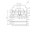
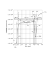
実施の形態にかかる炭化珪素半導体装置の構造について説明する。図1,2は、それぞれ、実施の形態にかかる炭化珪素半導体基板および炭化珪素半導体装置の構造を示す断面図である。図3は、図1の第1,2バッファ領域の不純物濃度分布を示す特性図である。図3には、第1バッファ領域11の狙いの厚さt1を1μmとし、第2バッファ領域12の狙いの厚さt2を7μmとした場合を示している。また、図3には、炭化珪素半導体基板20の両主面付近の不純物濃度分布を図示省略しており、n+型出発基板21およびn-型ドリフト領域2はそれぞれ一部(第1,2バッファ領域11,12との界面25,27付近)のみを図示している。
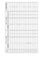
第1,2バッファ領域11,12の不純物濃度および厚さt1,t2とオン電圧Vonとの関係について検証した。図4は、実験例の第1,2バッファ領域の不純物濃度および厚さとオン電圧Vonとの関係を示す図表である。上述した実施の形態にかかる炭化珪素半導体装置10にしたがって、第1,2バッファ領域11,12の不純物濃度および厚さt1,t2をそれぞれ異なる設計条件(16条件:以下、試料No.1~No.16とする)とした各試料(SiC-MOSFET)をそれぞれ所定個数ずつ作製した(以下、実験例とする)。これらすべての試料のボディダイオードに同条件(1000A/cm2)で順方向電流を流した後に、SiC-MOSFETのオン電圧Vonを測定した。
2 n-型ドリフト領域
3 n型電流拡散領域
4 p型ベース領域
5 n+型ソース領域
6 p++型コンタクト領域
7 トレンチ
8 ゲート絶縁膜
9 ゲート電極
10 炭化珪素半導体装置
11 第1バッファ領域(n型バッファ領域)
12 第2バッファ領域(n+型バッファ領域)
13,14 p+型領域
15 層間絶縁膜
16 ソース電極
17 ドレイン電極
20 炭化珪素半導体基板
21 n+型出発基板
22~24,31,32 エピタキシャル層
25 n+型出発基板と第1バッファ領域との界面
26 第1バッファ領域と第2バッファ領域との界面
27 第2バッファ領域とn-型ドリフト領域との界面
30 半導体基板
33 pn接合
41~44 不純物濃度勾配
41a,41b,42a,43a,44a 不純物濃度分布の勾配変化点
t1 第1バッファ領域の厚さ
t2 第2バッファ領域の厚さ
t3 n-型ドリフト領域の厚さ
t10 第1バッファ領域と第2バッファ領域との総厚さ
Claims (15)
- 炭化珪素からなる出発基板にエピタキシャル層をエピタキシャル成長させた半導体基板の主面に垂直な方向に電流が流れる炭化珪素半導体装置であって、
前記エピタキシャル層の内部に設けられた第1導電型の第1半導体領域と、
前記エピタキシャル層の内部において前記第1半導体領域と前記出発基板との間に、前記出発基板に接して設けられた、前記第1半導体領域よりも不純物濃度が高く、かつ前記出発基板よりも不純物濃度が低い第1導電型の第2半導体領域と、
前記エピタキシャル層の内部において前記第1半導体領域と前記第2半導体領域との間に、前記第1半導体領域および前記第2半導体領域に接して設けられた、前記第2半導体領域よりも不純物濃度が高い第1導電型の第3半導体領域と、
を備え、
前記第3半導体領域の不純物濃度は、
前記第3半導体領域と前記第1半導体領域との第1界面に相対的に近い所定の第1深さ位置から、前記第2半導体領域と前記第3半導体領域との第2界面に相対的に近い所定の第2深さ位置へ向かうにしたがって第1不純物濃度勾配で連続的に増加し、前記第2深さ位置で最大不純物濃度となっており、
前記第1深さ位置から前記第1界面へ向かうにしたがって第2不純物濃度勾配で連続的に減少しており、
前記第2深さ位置から前記第2界面へ向かうにしたがって第3不純物濃度勾配で連続的に減少しており、
かつ前記出発基板の不純物濃度よりも低く、
前記第2不純物濃度勾配は、前記第3不純物濃度勾配よりも小さいことを特徴とする炭化珪素半導体装置。 - 前記第1不純物濃度勾配の絶対値は、前記第2不純物濃度勾配の絶対値および前記第3不純物濃度勾配の絶対値よりも小さいことを特徴とする請求項1に記載の炭化珪素半導体装置。
- 前記第3半導体領域の不純物濃度は、前記出発基板の不純物濃度の1/2以下であることを特徴とする請求項1に記載の炭化珪素半導体装置。
- 前記第3半導体領域の不純物濃度は、1.0×10¹⁸/cm3以上5.0×1018/cm3以下の範囲内であることを特徴とする請求項1に記載の炭化珪素半導体装置。
- 前記第3半導体領域の不純物濃度は、3.0×10¹⁸/cm3以上の範囲内であることを特徴とする請求項4に記載の炭化珪素半導体装置。
- 前記出発基板の不純物濃度は、1.0×10¹⁸/cm3以上1.0×1019/cm3以下の範囲内であることを特徴とする請求項1に記載の炭化珪素半導体装置。
- 前記第2半導体領域の不純物濃度は、0.5×10¹⁸/cm3以上1.5×1018/cm3以下の範囲内であることを特徴とする請求項1に記載の炭化珪素半導体装置。
- 前記第3半導体領域の厚さは、1μmよりも厚く7μm未満の範囲内であることを特徴とする請求項1に記載の炭化珪素半導体装置。
- 前記第2半導体領域の厚さは、1μmよりも厚く4μm以下の範囲内であることを特徴とする請求項8に記載の炭化珪素半導体装置。
- 前記第2半導体領域の厚さは、1μm以下であることを特徴とする請求項8に記載の炭化珪素半導体装置。
- 前記第2半導体領域の厚さは、1μmよりも厚く4μm以下の範囲内であることを特徴とする請求項1に記載の炭化珪素半導体装置。
- 前記第3半導体領域の厚さは、1μm以下であることを特徴とする請求項11に記載の炭化珪素半導体装置。
- 前記第2半導体領域と前記第3半導体領域との総厚さは、2μm以上8μm以下の範囲内であることを特徴とする請求項1に記載の炭化珪素半導体装置。
- 前記エピタキシャル層の内部において前記半導体基板の第1主面と前記第1半導体領域との間に設けられた第2導電型の第4半導体領域と、
前記エピタキシャル層の内部において前記半導体基板の第1主面と前記第4半導体領域との間に選択的に設けられた第1導電型の第5半導体領域と、
前記第4半導体領域の、前記第1半導体領域と前記第5半導体領域の間の領域に接して設けられたゲート絶縁膜と、
前記ゲート絶縁膜を挟んで前記第4半導体領域の反対側に設けられたゲート電極と、
前記半導体基板の前記エピタキシャル層で形成される第1主面に設けられ、前記第4半導体領域および前記第5半導体領域に電気的に接続された第1電極と、
前記半導体基板の前記出発基板で形成される第2主面に設けられ、前記出発基板に電気的に接続された第2電極と、
を備えることを特徴とする請求項1~13のいずれか一つに記載の炭化珪素半導体装置。 - 炭化珪素からなる出発基板にエピタキシャル層をエピタキシャル成長させた炭化珪素半導体基板であって、
前記エピタキシャル層の内部に設けられた第1導電型の第1半導体領域と、
前記エピタキシャル層の内部において前記第1半導体領域と前記出発基板との間に、前記出発基板に接して設けられた、前記第1半導体領域よりも不純物濃度が高く、かつ前記出発基板よりも不純物濃度が低い第1導電型の第2半導体領域と、
前記エピタキシャル層の内部において前記第1半導体領域と前記第2半導体領域との間に、前記第1半導体領域および前記第2半導体領域に接して設けられた、前記第2半導体領域よりも不純物濃度が高い第1導電型の第3半導体領域と、
を備え、
前記第3半導体領域の不純物濃度は、
前記第3半導体領域と前記第1半導体領域との第1界面に相対的に近い所定の第1深さ位置から、前記第2半導体領域と前記第3半導体領域との第2界面に相対的に近い所定の第2深さ位置へ向かうにしたがって第1不純物濃度勾配で連続的に増加し、前記第2深さ位置で最大不純物濃度となっており、
前記第1深さ位置から前記第1界面へ向かうにしたがって第2不純物濃度勾配で連続的に減少しており、
前記第2深さ位置から前記第2界面へ向かうにしたがって第3不純物濃度勾配で連続的に減少しており、
かつ前記出発基板の不純物濃度よりも低く、
前記第2不純物濃度勾配は、前記第3不純物濃度勾配よりも小さいことを特徴とする炭化珪素半導体基板。
Applications Claiming Priority (3)
| Application Number | Priority Date | Filing Date | Title |
|---|---|---|---|
| JP2021144110 | 2021-09-03 | ||
| JP2021144110 | 2021-09-03 | ||
| PCT/JP2022/026398 WO2023032455A1 (ja) | 2021-09-03 | 2022-06-30 | 炭化珪素半導体装置および炭化珪素半導体基板 |
Publications (3)
| Publication Number | Publication Date |
|---|---|
| JPWO2023032455A1 JPWO2023032455A1 (ja) | 2023-03-09 |
| JPWO2023032455A5 JPWO2023032455A5 (ja) | 2023-11-28 |
| JP7601240B2 true JP7601240B2 (ja) | 2024-12-17 |
Family
ID=85412116
Family Applications (1)
| Application Number | Title | Priority Date | Filing Date |
|---|---|---|---|
| JP2023545122A Active JP7601240B2 (ja) | 2021-09-03 | 2022-06-30 | 炭化珪素半導体装置および炭化珪素半導体基板 |
Country Status (4)
| Country | Link |
|---|---|
| US (2) | US12593499B2 (ja) |
| JP (1) | JP7601240B2 (ja) |
| CN (1) | CN116897434A (ja) |
| WO (1) | WO2023032455A1 (ja) |
Citations (2)
| Publication number | Priority date | Publication date | Assignee | Title |
|---|---|---|---|---|
| WO2017094764A1 (ja) | 2015-12-02 | 2017-06-08 | 三菱電機株式会社 | 炭化珪素エピタキシャル基板および炭化珪素半導体装置 |
| JP2019102493A (ja) | 2017-11-28 | 2019-06-24 | 富士電機株式会社 | 炭化珪素半導体装置および炭化珪素半導体装置の製造方法 |
Family Cites Families (12)
| Publication number | Priority date | Publication date | Assignee | Title |
|---|---|---|---|---|
| JP4568929B2 (ja) * | 1999-09-21 | 2010-10-27 | 株式会社デンソー | 炭化珪素半導体装置及びその製造方法 |
| DE102005046707B3 (de) * | 2005-09-29 | 2007-05-03 | Siced Electronics Development Gmbh & Co. Kg | SiC-PN-Leistungsdiode |
| JP5369464B2 (ja) * | 2008-03-24 | 2013-12-18 | 富士電機株式会社 | 炭化珪素mos型半導体装置 |
| EP2806461B1 (en) * | 2012-01-19 | 2021-11-24 | Fuji Electric Co., Ltd. | Semiconductor device and method for producing same |
| JP6337964B2 (ja) * | 2014-07-23 | 2018-06-06 | 富士電機株式会社 | 半導体装置および半導体装置の製造方法 |
| JP6550869B2 (ja) * | 2015-04-01 | 2019-07-31 | 富士電機株式会社 | 半導体装置 |
| DE102015208097B4 (de) * | 2015-04-30 | 2022-03-31 | Infineon Technologies Ag | Herstellen einer Halbleitervorrichtung durch Epitaxie |
| JP6547844B2 (ja) | 2015-12-18 | 2019-07-24 | 富士電機株式会社 | 炭化珪素半導体基板、炭化珪素半導体基板の製造方法、半導体装置および半導体装置の製造方法 |
| CN107851584B (zh) * | 2016-02-23 | 2021-06-11 | 富士电机株式会社 | 半导体装置 |
| CN110301034B (zh) | 2017-02-20 | 2023-07-11 | 株式会社博迈立铖 | 碳化硅层叠基板及其制造方法 |
| JP7275573B2 (ja) * | 2018-12-27 | 2023-05-18 | 富士電機株式会社 | 炭化珪素半導体装置および炭化珪素半導体装置の製造方法 |
| US20230049926A1 (en) * | 2021-08-13 | 2023-02-16 | Semiconductor Components Industries, Llc | Epitaxial field stop region for semiconductor devices |
-
2022
- 2022-06-30 WO PCT/JP2022/026398 patent/WO2023032455A1/ja not_active Ceased
- 2022-06-30 JP JP2023545122A patent/JP7601240B2/ja active Active
- 2022-06-30 CN CN202280016320.9A patent/CN116897434A/zh active Pending
-
2023
- 2023-08-23 US US18/454,147 patent/US12593499B2/en active Active
-
2026
- 2026-02-27 US US19/553,038 patent/US20260198072A1/en active Pending
Patent Citations (2)
| Publication number | Priority date | Publication date | Assignee | Title |
|---|---|---|---|---|
| WO2017094764A1 (ja) | 2015-12-02 | 2017-06-08 | 三菱電機株式会社 | 炭化珪素エピタキシャル基板および炭化珪素半導体装置 |
| JP2019102493A (ja) | 2017-11-28 | 2019-06-24 | 富士電機株式会社 | 炭化珪素半導体装置および炭化珪素半導体装置の製造方法 |
Also Published As
| Publication number | Publication date |
|---|---|
| WO2023032455A1 (ja) | 2023-03-09 |
| US20260198072A1 (en) | 2026-07-09 |
| US12593499B2 (en) | 2026-03-31 |
| US20230395709A1 (en) | 2023-12-07 |
| CN116897434A (zh) | 2023-10-17 |
| JPWO2023032455A1 (ja) | 2023-03-09 |
Similar Documents
| Publication | Publication Date | Title |
|---|---|---|
| US20250267902A1 (en) | Superjunction silicon carbide semiconductor device having parallel pn column structure with crystal defects | |
| JP6844163B2 (ja) | 炭化珪素半導体装置 | |
| JP5101985B2 (ja) | ジャンクションバリアショットキーダイオード | |
| US10418445B2 (en) | Silicon carbide semiconductor device and method of manufacturing a silicon carbide semiconductor device | |
| US8618557B2 (en) | Wide-band-gap reverse-blocking MOS-type semiconductor device | |
| JP5665912B2 (ja) | 半導体装置及びその製造方法 | |
| US11948976B2 (en) | Vertical MOSFET having trench gate structure containing silicon carbide | |
| WO2011033550A1 (ja) | 半導体装置 | |
| US9349797B2 (en) | SiC devices with high blocking voltage terminated by a negative bevel | |
| JP2014060376A (ja) | ショットキーバリアダイオードおよびその製造方法 | |
| JP2017508300A (ja) | ワイドバンドギャップ半導体材料用igbt構造 | |
| JP2022163554A (ja) | 炭化珪素半導体装置及びその製造方法 | |
| CN111697078A (zh) | 高雪崩耐量的vdmos器件及制备方法 | |
| JP7574575B2 (ja) | 炭化珪素半導体装置および炭化珪素半導体装置の製造方法 | |
| JP2018022852A (ja) | 半導体装置およびその製造方法 | |
| CN104838503A (zh) | 半导体装置 | |
| JP5682102B2 (ja) | 逆耐圧を有する縦型窒化ガリウム半導体装置 | |
| US12538538B2 (en) | Silicon carbide semiconductor device and silicon carbide semiconductor substrate | |
| JP5476439B2 (ja) | ジャンクションバリアショットキーダイオード | |
| JP5402220B2 (ja) | 炭化珪素半導体装置の製造方法および炭化珪素半導体装置 | |
| JP6930113B2 (ja) | 半導体装置および半導体装置の製造方法 | |
| JP2009054659A (ja) | 窒化ガリウム半導体装置の製造方法 | |
| US12593499B2 (en) | Silicon carbide semiconductor device and silicon carbide semiconductor substrate | |
| US9917180B2 (en) | Trenched and implanted bipolar junction transistor | |
| US20250324741A1 (en) | Silicon carbide semiconductor device and method of manufacturing the same |
Legal Events
| Date | Code | Title | Description |
|---|---|---|---|
| A524 | Written submission of copy of amendment under article 19 pct |
Free format text: JAPANESE INTERMEDIATE CODE: A527 Effective date: 20230830 |
|
| A621 | Written request for application examination |
Free format text: JAPANESE INTERMEDIATE CODE: A621 Effective date: 20230830 |
|
| TRDD | Decision of grant or rejection written | ||
| A01 | Written decision to grant a patent or to grant a registration (utility model) |
Free format text: JAPANESE INTERMEDIATE CODE: A01 Effective date: 20241105 |
|
| A61 | First payment of annual fees (during grant procedure) |
Free format text: JAPANESE INTERMEDIATE CODE: A61 Effective date: 20241118 |
|
| R150 | Certificate of patent or registration of utility model |
Ref document number: 7601240 Country of ref document: JP Free format text: JAPANESE INTERMEDIATE CODE: R150 |