JP7601553B2 - 放射線検出器及び放射線検出器の製造方法 - Google Patents
放射線検出器及び放射線検出器の製造方法 Download PDFInfo
- Publication number
- JP7601553B2 JP7601553B2 JP2019234435A JP2019234435A JP7601553B2 JP 7601553 B2 JP7601553 B2 JP 7601553B2 JP 2019234435 A JP2019234435 A JP 2019234435A JP 2019234435 A JP2019234435 A JP 2019234435A JP 7601553 B2 JP7601553 B2 JP 7601553B2
- Authority
- JP
- Japan
- Prior art keywords
- resin frame
- protective film
- scintillator layer
- scintillator
- film
- Prior art date
- Legal status (The legal status is an assumption and is not a legal conclusion. Google has not performed a legal analysis and makes no representation as to the accuracy of the status listed.)
- Active
Links
- 230000005855 radiation Effects 0.000 title claims description 127
- 238000000034 method Methods 0.000 title claims description 61
- 238000004519 manufacturing process Methods 0.000 title claims description 55
- 239000011347 resin Substances 0.000 claims description 292
- 229920005989 resin Polymers 0.000 claims description 292
- 230000001681 protective effect Effects 0.000 claims description 220
- 238000006243 chemical reaction Methods 0.000 claims description 106
- 230000000873 masking effect Effects 0.000 claims description 61
- 239000011248 coating agent Substances 0.000 claims description 45
- 238000000576 coating method Methods 0.000 claims description 45
- 239000000463 material Substances 0.000 claims description 43
- 238000005520 cutting process Methods 0.000 claims description 34
- 238000001514 detection method Methods 0.000 claims description 29
- 230000001678 irradiating effect Effects 0.000 claims description 12
- 238000010030 laminating Methods 0.000 claims description 2
- 239000010408 film Substances 0.000 description 350
- 230000000630 rising effect Effects 0.000 description 25
- 239000000758 substrate Substances 0.000 description 17
- 230000000694 effects Effects 0.000 description 14
- 230000015572 biosynthetic process Effects 0.000 description 11
- 238000010586 diagram Methods 0.000 description 11
- CURLTUGMZLYLDI-UHFFFAOYSA-N Carbon dioxide Chemical compound O=C=O CURLTUGMZLYLDI-UHFFFAOYSA-N 0.000 description 10
- -1 polyparaxylylene Polymers 0.000 description 10
- 229910052751 metal Inorganic materials 0.000 description 9
- 239000002184 metal Substances 0.000 description 9
- 239000000853 adhesive Substances 0.000 description 8
- 230000001070 adhesive effect Effects 0.000 description 8
- 230000002411 adverse Effects 0.000 description 8
- 229920000052 poly(p-xylylene) Polymers 0.000 description 8
- 230000002829 reductive effect Effects 0.000 description 8
- 230000002950 deficient Effects 0.000 description 7
- 230000002093 peripheral effect Effects 0.000 description 7
- 230000000052 comparative effect Effects 0.000 description 6
- 230000007423 decrease Effects 0.000 description 6
- 230000000149 penetrating effect Effects 0.000 description 6
- 229910052782 aluminium Inorganic materials 0.000 description 5
- XAGFODPZIPBFFR-UHFFFAOYSA-N aluminium Chemical compound [Al] XAGFODPZIPBFFR-UHFFFAOYSA-N 0.000 description 5
- 229910002092 carbon dioxide Inorganic materials 0.000 description 5
- 238000002161 passivation Methods 0.000 description 5
- 230000001133 acceleration Effects 0.000 description 4
- 239000001569 carbon dioxide Substances 0.000 description 4
- 238000005229 chemical vapour deposition Methods 0.000 description 4
- 230000007797 corrosion Effects 0.000 description 4
- 238000005260 corrosion Methods 0.000 description 4
- 230000036961 partial effect Effects 0.000 description 4
- 230000003287 optical effect Effects 0.000 description 3
- 239000004925 Acrylic resin Substances 0.000 description 2
- 229920000178 Acrylic resin Polymers 0.000 description 2
- 239000013078 crystal Substances 0.000 description 2
- 230000003247 decreasing effect Effects 0.000 description 2
- 230000006866 deterioration Effects 0.000 description 2
- 238000003475 lamination Methods 0.000 description 2
- 230000007257 malfunction Effects 0.000 description 2
- 238000001579 optical reflectometry Methods 0.000 description 2
- 230000035945 sensitivity Effects 0.000 description 2
- 229920002050 silicone resin Polymers 0.000 description 2
- 229910052709 silver Inorganic materials 0.000 description 2
- 239000004332 silver Substances 0.000 description 2
- 238000007740 vapor deposition Methods 0.000 description 2
- 239000011800 void material Substances 0.000 description 2
- XLYOFNOQVPJJNP-UHFFFAOYSA-N water Chemical compound O XLYOFNOQVPJJNP-UHFFFAOYSA-N 0.000 description 2
- 239000012463 white pigment Substances 0.000 description 2
- 229910052581 Si3N4 Inorganic materials 0.000 description 1
- VYPSYNLAJGMNEJ-UHFFFAOYSA-N Silicium dioxide Chemical compound O=[Si]=O VYPSYNLAJGMNEJ-UHFFFAOYSA-N 0.000 description 1
- BQCADISMDOOEFD-UHFFFAOYSA-N Silver Chemical compound [Ag] BQCADISMDOOEFD-UHFFFAOYSA-N 0.000 description 1
- GWEVSGVZZGPLCZ-UHFFFAOYSA-N Titan oxide Chemical compound O=[Ti]=O GWEVSGVZZGPLCZ-UHFFFAOYSA-N 0.000 description 1
- 238000010521 absorption reaction Methods 0.000 description 1
- 239000003522 acrylic cement Substances 0.000 description 1
- PNEYBMLMFCGWSK-UHFFFAOYSA-N aluminium oxide Inorganic materials [O-2].[O-2].[O-2].[Al+3].[Al+3] PNEYBMLMFCGWSK-UHFFFAOYSA-N 0.000 description 1
- 229910021417 amorphous silicon Inorganic materials 0.000 description 1
- 238000003491 array Methods 0.000 description 1
- 230000005540 biological transmission Effects 0.000 description 1
- 229910052804 chromium Inorganic materials 0.000 description 1
- 238000011109 contamination Methods 0.000 description 1
- 230000006378 damage Effects 0.000 description 1
- 238000000151 deposition Methods 0.000 description 1
- 230000008021 deposition Effects 0.000 description 1
- 238000005516 engineering process Methods 0.000 description 1
- 239000011521 glass Substances 0.000 description 1
- PCHJSUWPFVWCPO-UHFFFAOYSA-N gold Chemical compound [Au] PCHJSUWPFVWCPO-UHFFFAOYSA-N 0.000 description 1
- 229910052737 gold Inorganic materials 0.000 description 1
- 239000010931 gold Substances 0.000 description 1
- 238000010438 heat treatment Methods 0.000 description 1
- 238000007689 inspection Methods 0.000 description 1
- 239000007788 liquid Substances 0.000 description 1
- 238000012986 modification Methods 0.000 description 1
- 230000004048 modification Effects 0.000 description 1
- SIWVEOZUMHYXCS-UHFFFAOYSA-N oxo(oxoyttriooxy)yttrium Chemical compound O=[Y]O[Y]=O SIWVEOZUMHYXCS-UHFFFAOYSA-N 0.000 description 1
- RVTZCBVAJQQJTK-UHFFFAOYSA-N oxygen(2-);zirconium(4+) Chemical compound [O-2].[O-2].[Zr+4] RVTZCBVAJQQJTK-UHFFFAOYSA-N 0.000 description 1
- 239000000049 pigment Substances 0.000 description 1
- 230000002441 reversible effect Effects 0.000 description 1
- 239000004065 semiconductor Substances 0.000 description 1
- 229910052710 silicon Inorganic materials 0.000 description 1
- HQVNEWCFYHHQES-UHFFFAOYSA-N silicon nitride Chemical compound N12[Si]34N5[Si]62N3[Si]51N64 HQVNEWCFYHHQES-UHFFFAOYSA-N 0.000 description 1
- 229910052814 silicon oxide Inorganic materials 0.000 description 1
- 239000007787 solid Substances 0.000 description 1
- 230000003685 thermal hair damage Effects 0.000 description 1
- 239000010409 thin film Substances 0.000 description 1
- 230000009974 thixotropic effect Effects 0.000 description 1
- 229910052719 titanium Inorganic materials 0.000 description 1
- 239000010936 titanium Substances 0.000 description 1
- OGIDPMRJRNCKJF-UHFFFAOYSA-N titanium oxide Inorganic materials [Ti]=O OGIDPMRJRNCKJF-UHFFFAOYSA-N 0.000 description 1
- 229910001928 zirconium oxide Inorganic materials 0.000 description 1
Images


Classifications
-
- G—PHYSICS
- G01—MEASURING; TESTING
- G01T—MEASUREMENT OF NUCLEAR OR X-RADIATION
- G01T1/00—Measuring X-radiation, gamma radiation, corpuscular radiation, or cosmic radiation
- G01T1/16—Measuring radiation intensity
- G01T1/20—Measuring radiation intensity with scintillation detectors
- G01T1/2018—Scintillation-photodiode combinations
- G01T1/20188—Auxiliary details, e.g. casings or cooling
- G01T1/20189—Damping or insulation against damage, e.g. caused by heat or pressure
-
- G—PHYSICS
- G01—MEASURING; TESTING
- G01T—MEASUREMENT OF NUCLEAR OR X-RADIATION
- G01T1/00—Measuring X-radiation, gamma radiation, corpuscular radiation, or cosmic radiation
- G01T1/16—Measuring radiation intensity
- G01T1/20—Measuring radiation intensity with scintillation detectors
- G01T1/2018—Scintillation-photodiode combinations
- G01T1/20181—Stacked detectors, e.g. for measuring energy and positional information
-
- G—PHYSICS
- G01—MEASURING; TESTING
- G01T—MEASUREMENT OF NUCLEAR OR X-RADIATION
- G01T1/00—Measuring X-radiation, gamma radiation, corpuscular radiation, or cosmic radiation
- G01T1/16—Measuring radiation intensity
- G01T1/20—Measuring radiation intensity with scintillation detectors
- G01T1/2002—Optical details, e.g. reflecting or diffusing layers
-
- G—PHYSICS
- G01—MEASURING; TESTING
- G01T—MEASUREMENT OF NUCLEAR OR X-RADIATION
- G01T1/00—Measuring X-radiation, gamma radiation, corpuscular radiation, or cosmic radiation
- G01T1/16—Measuring radiation intensity
- G01T1/20—Measuring radiation intensity with scintillation detectors
- G01T1/2018—Scintillation-photodiode combinations
- G01T1/20188—Auxiliary details, e.g. casings or cooling
-
- G—PHYSICS
- G01—MEASURING; TESTING
- G01T—MEASUREMENT OF NUCLEAR OR X-RADIATION
- G01T1/00—Measuring X-radiation, gamma radiation, corpuscular radiation, or cosmic radiation
- G01T1/16—Measuring radiation intensity
- G01T1/20—Measuring radiation intensity with scintillation detectors
- G01T1/202—Measuring radiation intensity with scintillation detectors the detector being a crystal
-
- H—ELECTRICITY
- H10—SEMICONDUCTOR DEVICES; ELECTRIC SOLID-STATE DEVICES NOT OTHERWISE PROVIDED FOR
- H10F—INORGANIC SEMICONDUCTOR DEVICES SENSITIVE TO INFRARED RADIATION, LIGHT, ELECTROMAGNETIC RADIATION OF SHORTER WAVELENGTH OR CORPUSCULAR RADIATION
- H10F39/00—Integrated devices, or assemblies of multiple devices, comprising at least one element covered by group H10F30/00, e.g. radiation detectors comprising photodiode arrays
- H10F39/011—Manufacture or treatment of image sensors covered by group H10F39/12
-
- H—ELECTRICITY
- H10—SEMICONDUCTOR DEVICES; ELECTRIC SOLID-STATE DEVICES NOT OTHERWISE PROVIDED FOR
- H10F—INORGANIC SEMICONDUCTOR DEVICES SENSITIVE TO INFRARED RADIATION, LIGHT, ELECTROMAGNETIC RADIATION OF SHORTER WAVELENGTH OR CORPUSCULAR RADIATION
- H10F39/00—Integrated devices, or assemblies of multiple devices, comprising at least one element covered by group H10F30/00, e.g. radiation detectors comprising photodiode arrays
- H10F39/10—Integrated devices
- H10F39/12—Image sensors
- H10F39/18—Complementary metal-oxide-semiconductor [CMOS] image sensors; Photodiode array image sensors
- H10F39/189—X-ray, gamma-ray or corpuscular radiation imagers
- H10F39/1898—Indirect radiation image sensors, e.g. using luminescent members
-
- H—ELECTRICITY
- H10—SEMICONDUCTOR DEVICES; ELECTRIC SOLID-STATE DEVICES NOT OTHERWISE PROVIDED FOR
- H10F—INORGANIC SEMICONDUCTOR DEVICES SENSITIVE TO INFRARED RADIATION, LIGHT, ELECTROMAGNETIC RADIATION OF SHORTER WAVELENGTH OR CORPUSCULAR RADIATION
- H10F39/00—Integrated devices, or assemblies of multiple devices, comprising at least one element covered by group H10F30/00, e.g. radiation detectors comprising photodiode arrays
- H10F39/80—Constructional details of image sensors
- H10F39/811—Interconnections
Landscapes
- Physics & Mathematics (AREA)
- Health & Medical Sciences (AREA)
- Life Sciences & Earth Sciences (AREA)
- General Physics & Mathematics (AREA)
- High Energy & Nuclear Physics (AREA)
- Molecular Biology (AREA)
- Spectroscopy & Molecular Physics (AREA)
- Chemical & Material Sciences (AREA)
- Crystallography & Structural Chemistry (AREA)
- Measurement Of Radiation (AREA)
Description
次に、図8~図18を参照して、本実施形態に係る放射線検出器1の製造方法について説明する。まず、図8(a)に示すように、光電変換素子アレイ7を準備する(工程S1)。続いて、図8(b)に示すように、シンチレータ層8を形成(積層)する(工程S2)。具体的には、光電変換素子アレイ7上の受光部3を覆う領域において、TlをドープしたCsIの柱状結晶を例えば蒸着法により成長させる。CsIの柱状結晶の厚さは、一例として600μm程度である。
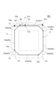
放射線検出器1は、一次元又は二次元に配列された複数の光電変換素子3aを含む受光部3、及び光電変換素子3aと電気的に接続され且つ受光部3の外側に配置された複数のボンディングパッド5を有する光電変換素子アレイ7と、受光部3を覆うように光電変換素子アレイ7上に積層され、放射線を光に変換するシンチレータ層8と、シンチレータ層8の積層方向Aから見た場合に、シンチレータ層8及びボンディングパッド5から離間してシンチレータ層8とボンディングパッド5との間を通り且つシンチレータ層8を包囲するように、光電変換素子アレイ7上に形成された樹脂枠9と、シンチレータ層8を覆い、樹脂枠9上に位置する外縁13aを有する保護膜13と、を備える。樹脂枠9には、保護膜13の外縁13aと連続する溝30が形成され、溝30は、溝30の延在方向に対して交差する方向において部分的に重複する第1の溝端部32及び第2の溝端部33を含む重複領域31を有する。
次に、第2実施形態の放射線検出器1Aと放射線検出器1Aの製造方法について説明する。第1実施形態の放射線検出器1は、パネル保護部として樹脂枠9を用いていた。具体的には、放射線検出器1の製造時において、保護膜13を切断する際にレーザ光から光電変換素子アレイ7を保護する部材として樹脂枠9を用いた。そして、放射線検出器1は、樹脂枠9を構成要素として備えていた。
放射線検出器1Aの作用効果について説明する。放射線検出器1Aにおいて、シンチレータ層8を覆う保護膜20の外縁部22は、光電変換素子アレイ7と密着する密着部23を有する。これにより、保護膜20と光電変換素子アレイ7との間を通りシンチレータ層8に向かって湿気が入り込むことを防ぐことができる。さらに、保護膜20の外縁部22は、延在部24を有する。延在部24は、密着部23から光電変換素子アレイ7の反対側に自立状態で延在する。保護膜20の外縁部22が延在部24を有さないと保護膜20の外縁端20aが密着部23に含まれる。その場合、特に、密着部23のうち保護膜20の外縁端20aが位置する部分と光電変換素子アレイ7との密着性が確保しにくくなる。その結果、密着部23と光電変換素子アレイ7との界面からシンチレータ層8に湿気が侵入しやすくなる。
次に、図23~図28を参照して、放射線検出器1Aの製造方法の各工程について説明する。まず、図23(a)に示すように、光電変換素子アレイ7を用意する(工程S11)。次に、図23(b)に示すように、受光部3を覆うように光電変換素子アレイ7上にシンチレータ層8を設ける(工程S12)。
放射線検出器1Aの製造方法において、パネル保護部は、マスキング部材M1である。マスキング部材M1を配置する工程S13では、シンチレータ層8とボンディングパッド5との間の領域K、及びボンディングパッド5を覆うように、光電変換素子アレイ7上にマスキング部材M1を配置する。保護膜20を形成する工程S14では、光電変換素子アレイ7におけるシンチレータ層8が積層される側の表面全体及びマスキング部材M1の表面に保護膜20を形成する。この工程S14によれば、樹脂枠9を備えない放射線検出器1Aを製造することができる。つまり、シンチレータ層8とボンディングパッド5との間の距離を縮めることが可能になるので、放射線検出器1Aをさらに小型化することができる。
第1実施形態では、レーザ光によって樹脂枠9に過剰な深さの溝が形成されることを抑制した。同様に、第2実施形態では、レーザ光によってマスキング部材M1に過剰な深さの溝が形成されることを抑制した。これらの過剰な深さの溝は、いずれも樹脂枠9及びマスキング部材M1に対して過剰な大きさのエネルギが照射されることに起因する。この過剰な大きさのエネルギの照射は、樹脂枠9及びマスキング部材M1といった被照射体の同じ位置に複数回のレーザ光の照射がなされることがそのひとつの要因である。そこで、第1実施形態及び第2実施形態では、同じ位置に複数回のレーザ光の照射が行われないように、走査ラインをずらす手法を提示した。
第3実施形態で示した課題は、第3実施形態で示した制御の態様とは別の制御の態様によっても解決できる。第3実施形態の冒頭で説明した課題は、レーザ光の照射を開始するタイミングとレーザ光ヘッドの移動を開始するタイミングとが同時であることを前提にしていた。例えば、レーザ光の照射を開始するタイミングとレーザ光ヘッドの移動を開始するタイミングとをずらすことにより、被照射体への過剰な大きさのエネルギの照射を防止することができる。
Claims (15)
- 一次元又は二次元に配列された複数の光電変換素子を含む受光部、及び前記光電変換素子と電気的に接続され且つ前記受光部の外側に配置された複数のボンディングパッドを有する光検出パネルと、
前記受光部を覆うように前記光検出パネル上に積層され、放射線を光に変換するシンチレータ層と、
前記シンチレータ層の積層方向から見た場合に、前記シンチレータ層及び前記ボンディングパッドから離間して前記シンチレータ層と前記ボンディングパッドとの間を通り且つ前記シンチレータ層を包囲するように、前記光検出パネル上に形成された樹脂枠と、
前記シンチレータ層を覆い、前記樹脂枠上に位置する外縁を有するシンチレータ保護膜と、を備え、
前記樹脂枠には、前記シンチレータ保護膜の外縁と連続する溝が形成され、
前記溝は、前記溝の延在方向に対して交差する方向において部分的に重複する第1の溝端部及び第2の溝端部を含む重複領域を有し、
前記重複領域において前記シンチレータ層側に位置する前記第1の溝端部の外側の一部は、前記ボンディングパッド側に位置する前記第2の溝端部の内側の一部と重複する、放射線検出器。 - 前記シンチレータ保護膜の前記外縁を覆う被覆樹脂をさらに備える、請求項1に記載の放射線検出器。
- 前記被覆樹脂は、前記樹脂枠をさらに覆い、
前記被覆樹脂は、前記被覆樹脂と前記樹脂枠との接触面の縁部が前記樹脂枠上に形成されるように、前記樹脂枠に留まることが可能な材料特性を有する、請求項2に記載の放射線検出器。 - 前記樹脂枠の中央部は、前記樹脂枠の両縁部よりも高く、
前記溝の位置は、前記樹脂枠上において前記ボンディングパッド側に偏っている、請求項2又は3に記載の放射線検出器。 - 前記樹脂枠の幅は、700マイクロメートル以上であり、且つ、1000マイクロメートル以下である、請求項1~4の何れか一項に記載の放射線検出器。
- 前記樹脂枠の高さは、100マイクロメートル以上であり、且つ、300マイクロメートル以下である、請求項1~5の何れか一項に記載の放射線検出器。
- 前記光検出パネルの形状は、矩形であり、
前記樹脂枠は、前記シンチレータ層を包囲する4個の辺部を有し、
前記重複領域は、4個の前記辺部の何れかに設けられている、請求項1~6の何れか一項に記載の放射線検出器。 - 一次元又は二次元に配列された複数の光電変換素子を含む受光部、及び前記光電変換素子と電気的に接続され且つ前記受光部の外側に配置された複数のボンディングパッドを有する光検出パネルを準備し、放射線を光に変換するシンチレータ層を、前記受光部を覆うように前記光検出パネル上に積層する工程と、
前記シンチレータ層の積層方向から見た場合に、前記シンチレータ層を包囲するように、前記光検出パネル上にパネル保護部を配置する工程と、
前記シンチレータ層の表面、前記光検出パネルの前記シンチレータ層が積層される側の表面全体及び前記パネル保護部の表面を覆うように、シンチレータ保護膜となる膜を形成する工程と、
前記パネル保護部に沿ってレーザ光を照射することにより、前記シンチレータ保護膜となる膜を切断する工程と、
前記シンチレータ保護膜となる膜の外側の部分を除去する工程と、を有し、
前記シンチレータ保護膜となる膜を切断する工程では、前記シンチレータ保護膜となる膜の切断に起因して前記シンチレータ保護膜の外縁が形成され、前記パネル保護部には前記シンチレータ保護膜の外縁と連続する溝が形成されると共に、前記溝の延在方向に対して交差する方向において部分的に重複する第1の溝端部及び第2の溝端部を含む重複領域を前記溝が有するように、前記レーザ光を照射する動作において、前記ボンディングパッド側に位置する前記第1の溝端部を形成するときに、前記シンチレータ層側に位置する前記第2の溝端部の外側における前記シンチレータ保護膜となる膜を介して未加工の前記パネル保護部の表面に前記レーザ光が照射される、放射線検出器の製造方法。 - 前記光検出パネルの形状は、矩形であり、
前記パネル保護部は、前記シンチレータ層を包囲する4個の辺部を有し、
前記シンチレータ保護膜となる膜を切断する工程では、4個の前記辺部の何れかに前記重複領域を設ける、請求項8に記載の放射線検出器の製造方法。 - 前記シンチレータ保護膜となる膜を切断する工程は、
4個の前記辺部が構成する4個の角部の位置のうち少なくとも1個を基準位置に設定する工程と、
前記基準位置に基づいて、4個の前記辺部のそれぞれに前記レーザ光を照射する工程と、を含む、請求項9に記載の放射線検出器の製造方法。 - 前記パネル保護部は、樹脂枠であり、
前記パネル保護部を配置する工程では、前記シンチレータ層及び前記ボンディングパッドから離間して前記シンチレータ層と前記ボンディングパッドとの間を通り且つ前記シンチレータ層を包囲するように、前記光検出パネル上に前記樹脂枠を配置する、請求項8~10の何れか一項に記載の放射線検出器の製造方法。 - 前記パネル保護部を配置する工程では、前記樹脂枠の中央部が前記樹脂枠の両縁部よりも高くなるように前記樹脂枠を形成し、
前記シンチレータ保護膜となる膜を切断する工程では、前記樹脂枠上において前記ボンディングパッド側に偏った位置に前記レーザ光を照射する、請求項11に記載の放射線検出器の製造方法。 - 前記パネル保護部は、マスキング部材であり、
前記パネル保護部を配置する工程では、前記シンチレータ層と前記ボンディングパッドとの間の領域における外側の領域、及び前記ボンディングパッドを覆うように、前記光検出パネル上に前記マスキング部材を配置し、
前記シンチレータ保護膜となる膜を形成する工程では、前記シンチレータ層の表面、前記光検出パネルの前記シンチレータ層が積層される側の表面全体及び前記マスキング部材の表面に前記シンチレータ保護膜となる膜を形成する、請求項8~10の何れか一項に記載の放射線検出器の製造方法。 - 前記シンチレータ保護膜となる膜の外側の部分を除去する工程の後に、前記マスキング部材を除去する工程をさらに含む、請求項13に記載の放射線検出器の製造方法。
- 前記シンチレータ保護膜となる膜の外側の部分を除去する工程の後に、前記シンチレータ保護膜の前記外縁を覆う被覆樹脂を形成する工程をさらに有する、請求項13又は14に記載の放射線検出器の製造方法。
Priority Applications (7)
| Application Number | Priority Date | Filing Date | Title |
|---|---|---|---|
| JP2019234435A JP7601553B2 (ja) | 2019-12-25 | 2019-12-25 | 放射線検出器及び放射線検出器の製造方法 |
| US17/787,673 US11762110B2 (en) | 2019-12-25 | 2020-10-12 | Radiation detector and method for manufacturing radiation detector |
| PCT/JP2020/038533 WO2021131239A1 (ja) | 2019-12-25 | 2020-10-12 | 放射線検出器及び放射線検出器の製造方法 |
| KR1020227008448A KR102916405B1 (ko) | 2019-12-25 | 2020-10-12 | 방사선 검출기 및 방사선 검출기의 제조 방법 |
| EP20907868.2A EP4083662B1 (en) | 2019-12-25 | 2020-10-12 | Radiation detector and method for manufacturing radiation detector |
| CN202080089699.7A CN114868040B (zh) | 2019-12-25 | 2020-10-12 | 放射线检测器及放射线检测器的制造方法 |
| TW109136628A TWI865635B (zh) | 2019-12-25 | 2020-10-22 | 放射線檢測器及放射線檢測器的製造方法 |
Applications Claiming Priority (1)
| Application Number | Priority Date | Filing Date | Title |
|---|---|---|---|
| JP2019234435A JP7601553B2 (ja) | 2019-12-25 | 2019-12-25 | 放射線検出器及び放射線検出器の製造方法 |
Publications (2)
| Publication Number | Publication Date |
|---|---|
| JP2021103122A JP2021103122A (ja) | 2021-07-15 |
| JP7601553B2 true JP7601553B2 (ja) | 2024-12-17 |
Family
ID=76574227
Family Applications (1)
| Application Number | Title | Priority Date | Filing Date |
|---|---|---|---|
| JP2019234435A Active JP7601553B2 (ja) | 2019-12-25 | 2019-12-25 | 放射線検出器及び放射線検出器の製造方法 |
Country Status (7)
| Country | Link |
|---|---|
| US (1) | US11762110B2 (ja) |
| EP (1) | EP4083662B1 (ja) |
| JP (1) | JP7601553B2 (ja) |
| KR (1) | KR102916405B1 (ja) |
| CN (1) | CN114868040B (ja) |
| TW (1) | TWI865635B (ja) |
| WO (1) | WO2021131239A1 (ja) |
Citations (1)
| Publication number | Priority date | Publication date | Assignee | Title |
|---|---|---|---|---|
| JP3077941B2 (ja) | 1997-02-14 | 2000-08-21 | 浜松ホトニクス株式会社 | 放射線検出素子及びその製造方法 |
Family Cites Families (19)
| Publication number | Priority date | Publication date | Assignee | Title |
|---|---|---|---|---|
| NL7409191A (nl) * | 1974-07-08 | 1976-01-12 | Philips Nv | Verschilversterker. |
| US6586702B2 (en) * | 1997-09-25 | 2003-07-01 | Laser Electro Optic Application Technology Company | High density pixel array and laser micro-milling method for fabricating array |
| EP1258738B1 (en) * | 2000-01-13 | 2011-08-03 | Hamamatsu Photonics K.K. | Radiation image sensor and scintillator panel |
| EP1779140B1 (en) * | 2004-08-10 | 2018-06-20 | Canon Kabushiki Kaisha | Radiation detecting apparatus, scintillator panel, their manufacturing method and radiation detecting system |
| KR101058548B1 (ko) * | 2009-03-27 | 2011-08-23 | (주)하드램 | 레이저를 이용하는 다중 절단방법 |
| WO2011093431A1 (ja) * | 2010-01-29 | 2011-08-04 | 京セラ株式会社 | 光電変換装置およびその製造方法 |
| KR20110113482A (ko) * | 2010-04-09 | 2011-10-17 | (주)비엠알테크놀러지 | 직접 증착 방식에 의한 방사선 이미지 센서의 제조방법 |
| JP5739683B2 (ja) | 2011-02-03 | 2015-06-24 | 浜松ホトニクス株式会社 | シンチレータ、放射線検出器、及びシンチレータの製造方法 |
| KR101266554B1 (ko) * | 2011-05-09 | 2013-05-27 | 주식회사 아비즈알 | 신틸레이터 패널 및 신틸레이터 패널을 제조하는 방법 |
| CN104854645B (zh) * | 2012-12-18 | 2017-05-24 | 住友化学株式会社 | 光学显示设备的生产方法以及光学显示设备的生产系统 |
| JP6226579B2 (ja) * | 2013-06-13 | 2017-11-08 | 東芝電子管デバイス株式会社 | 放射線検出器及びその製造方法 |
| JP2015096823A (ja) | 2013-11-15 | 2015-05-21 | 浜松ホトニクス株式会社 | 放射線検出器、及び放射線検出器の製造方法 |
| JP6246056B2 (ja) * | 2014-04-23 | 2017-12-13 | 三菱電機株式会社 | 半導体デバイスの製造方法および半導体デバイスの製造装置 |
| JP6523620B2 (ja) * | 2014-06-16 | 2019-06-05 | キヤノン電子管デバイス株式会社 | 放射線検出器及びその製造方法 |
| JP6349277B2 (ja) * | 2014-12-17 | 2018-06-27 | トリニティ工業株式会社 | 加飾部品の製造方法、加飾部品 |
| JP6487263B2 (ja) * | 2015-04-20 | 2019-03-20 | 浜松ホトニクス株式会社 | 放射線検出器及びその製造方法 |
| JP6535769B2 (ja) * | 2018-01-26 | 2019-06-26 | 浜松ホトニクス株式会社 | 放射線検出器の製造方法 |
| CN108666374B (zh) * | 2018-05-18 | 2020-03-17 | 通威太阳能(安徽)有限公司 | 一种背面钝化矩阵点式激光开槽导电结构 |
| JP2019164163A (ja) * | 2019-06-03 | 2019-09-26 | 浜松ホトニクス株式会社 | 放射線検出器 |
-
2019
- 2019-12-25 JP JP2019234435A patent/JP7601553B2/ja active Active
-
2020
- 2020-10-12 WO PCT/JP2020/038533 patent/WO2021131239A1/ja not_active Ceased
- 2020-10-12 CN CN202080089699.7A patent/CN114868040B/zh active Active
- 2020-10-12 US US17/787,673 patent/US11762110B2/en active Active
- 2020-10-12 KR KR1020227008448A patent/KR102916405B1/ko active Active
- 2020-10-12 EP EP20907868.2A patent/EP4083662B1/en active Active
- 2020-10-22 TW TW109136628A patent/TWI865635B/zh active
Patent Citations (1)
| Publication number | Priority date | Publication date | Assignee | Title |
|---|---|---|---|---|
| JP3077941B2 (ja) | 1997-02-14 | 2000-08-21 | 浜松ホトニクス株式会社 | 放射線検出素子及びその製造方法 |
Also Published As
| Publication number | Publication date |
|---|---|
| EP4083662B1 (en) | 2026-01-28 |
| JP2021103122A (ja) | 2021-07-15 |
| CN114868040B (zh) | 2025-11-11 |
| TWI865635B (zh) | 2024-12-11 |
| TW202142893A (zh) | 2021-11-16 |
| KR20220118394A (ko) | 2022-08-25 |
| US20230011816A1 (en) | 2023-01-12 |
| CN114868040A (zh) | 2022-08-05 |
| KR102916405B1 (ko) | 2026-01-23 |
| EP4083662A4 (en) | 2024-01-10 |
| US11762110B2 (en) | 2023-09-19 |
| WO2021131239A1 (ja) | 2021-07-01 |
| EP4083662A1 (en) | 2022-11-02 |
Similar Documents
| Publication | Publication Date | Title |
|---|---|---|
| US11506799B2 (en) | Radiation detector, and method for producing radiation detector | |
| JP6487263B2 (ja) | 放射線検出器及びその製造方法 | |
| JP7601553B2 (ja) | 放射線検出器及び放射線検出器の製造方法 | |
| JP6535769B2 (ja) | 放射線検出器の製造方法 | |
| JP2019164163A (ja) | 放射線検出器 | |
| JP7345385B2 (ja) | 放射線検出器及び放射線検出器の製造方法 | |
| JP2020177033A (ja) | 放射線検出器 |
Legal Events
| Date | Code | Title | Description |
|---|---|---|---|
| A621 | Written request for application examination |
Free format text: JAPANESE INTERMEDIATE CODE: A621 Effective date: 20220929 |
|
| A131 | Notification of reasons for refusal |
Free format text: JAPANESE INTERMEDIATE CODE: A131 Effective date: 20230606 |
|
| A521 | Request for written amendment filed |
Free format text: JAPANESE INTERMEDIATE CODE: A523 Effective date: 20230713 |
|
| A02 | Decision of refusal |
Free format text: JAPANESE INTERMEDIATE CODE: A02 Effective date: 20230815 |
|
| A521 | Request for written amendment filed |
Free format text: JAPANESE INTERMEDIATE CODE: A523 Effective date: 20241025 |
|
| A61 | First payment of annual fees (during grant procedure) |
Free format text: JAPANESE INTERMEDIATE CODE: A61 Effective date: 20241205 |
|
| R150 | Certificate of patent or registration of utility model |
Ref document number: 7601553 Country of ref document: JP Free format text: JAPANESE INTERMEDIATE CODE: R150 |