JP7601696B2 - フォトダイオードアレイ及びイメージセンサ - Google Patents
フォトダイオードアレイ及びイメージセンサ Download PDFInfo
- Publication number
- JP7601696B2 JP7601696B2 JP2021069804A JP2021069804A JP7601696B2 JP 7601696 B2 JP7601696 B2 JP 7601696B2 JP 2021069804 A JP2021069804 A JP 2021069804A JP 2021069804 A JP2021069804 A JP 2021069804A JP 7601696 B2 JP7601696 B2 JP 7601696B2
- Authority
- JP
- Japan
- Prior art keywords
- electrode
- photodiode array
- gate
- plan
- line
- Prior art date
- Legal status (The legal status is an assumption and is not a legal conclusion. Google has not performed a legal analysis and makes no representation as to the accuracy of the status listed.)
- Active
Links
- 239000004020 conductor Substances 0.000 claims description 100
- 238000006243 chemical reaction Methods 0.000 claims description 16
- 239000000758 substrate Substances 0.000 claims description 16
- 239000000463 material Substances 0.000 claims description 4
- 239000011159 matrix material Substances 0.000 claims description 3
- 239000010410 layer Substances 0.000 description 89
- 239000010409 thin film Substances 0.000 description 39
- 239000011229 interlayer Substances 0.000 description 31
- 239000004065 semiconductor Substances 0.000 description 25
- 238000005513 bias potential Methods 0.000 description 15
- 229910021417 amorphous silicon Inorganic materials 0.000 description 14
- 238000001514 detection method Methods 0.000 description 11
- 238000004519 manufacturing process Methods 0.000 description 6
- 230000003071 parasitic effect Effects 0.000 description 6
- XUIMIQQOPSSXEZ-UHFFFAOYSA-N Silicon Chemical compound [Si] XUIMIQQOPSSXEZ-UHFFFAOYSA-N 0.000 description 5
- 230000007423 decrease Effects 0.000 description 5
- 239000010408 film Substances 0.000 description 5
- 229910052710 silicon Inorganic materials 0.000 description 5
- 239000010703 silicon Substances 0.000 description 5
- 238000010586 diagram Methods 0.000 description 4
- 239000012212 insulator Substances 0.000 description 4
- 239000002184 metal Substances 0.000 description 4
- 229910052751 metal Inorganic materials 0.000 description 4
- 238000002161 passivation Methods 0.000 description 4
- 229910045601 alloy Inorganic materials 0.000 description 3
- 239000000956 alloy Substances 0.000 description 3
- 229910052750 molybdenum Inorganic materials 0.000 description 3
- 238000003491 array Methods 0.000 description 2
- 239000003990 capacitor Substances 0.000 description 2
- 230000000694 effects Effects 0.000 description 2
- 239000011521 glass Substances 0.000 description 2
- 238000000034 method Methods 0.000 description 2
- 229910021420 polycrystalline silicon Inorganic materials 0.000 description 2
- 229920005591 polysilicon Polymers 0.000 description 2
- 230000005855 radiation Effects 0.000 description 2
- 229910052719 titanium Inorganic materials 0.000 description 2
- 206010047571 Visual impairment Diseases 0.000 description 1
- 229910052782 aluminium Inorganic materials 0.000 description 1
- 239000000969 carrier Substances 0.000 description 1
- 229910052804 chromium Inorganic materials 0.000 description 1
- 230000009977 dual effect Effects 0.000 description 1
- 238000005516 engineering process Methods 0.000 description 1
- 229910052733 gallium Inorganic materials 0.000 description 1
- 230000012447 hatching Effects 0.000 description 1
- 238000003384 imaging method Methods 0.000 description 1
- 239000012535 impurity Substances 0.000 description 1
- 229910052738 indium Inorganic materials 0.000 description 1
- 230000006698 induction Effects 0.000 description 1
- 238000009659 non-destructive testing Methods 0.000 description 1
- 238000002601 radiography Methods 0.000 description 1
- 239000011347 resin Substances 0.000 description 1
- 229920005989 resin Polymers 0.000 description 1
- 229920006395 saturated elastomer Polymers 0.000 description 1
- 239000002356 single layer Substances 0.000 description 1
- 229910052725 zinc Inorganic materials 0.000 description 1
Images








Classifications
-
- H—ELECTRICITY
- H10—SEMICONDUCTOR DEVICES; ELECTRIC SOLID-STATE DEVICES NOT OTHERWISE PROVIDED FOR
- H10F—INORGANIC SEMICONDUCTOR DEVICES SENSITIVE TO INFRARED RADIATION, LIGHT, ELECTROMAGNETIC RADIATION OF SHORTER WAVELENGTH OR CORPUSCULAR RADIATION
- H10F39/00—Integrated devices, or assemblies of multiple devices, comprising at least one element covered by group H10F30/00, e.g. radiation detectors comprising photodiode arrays
- H10F39/10—Integrated devices
- H10F39/12—Image sensors
- H10F39/18—Complementary metal-oxide-semiconductor [CMOS] image sensors; Photodiode array image sensors
-
- H—ELECTRICITY
- H10—SEMICONDUCTOR DEVICES; ELECTRIC SOLID-STATE DEVICES NOT OTHERWISE PROVIDED FOR
- H10F—INORGANIC SEMICONDUCTOR DEVICES SENSITIVE TO INFRARED RADIATION, LIGHT, ELECTROMAGNETIC RADIATION OF SHORTER WAVELENGTH OR CORPUSCULAR RADIATION
- H10F39/00—Integrated devices, or assemblies of multiple devices, comprising at least one element covered by group H10F30/00, e.g. radiation detectors comprising photodiode arrays
- H10F39/80—Constructional details of image sensors
- H10F39/802—Geometry or disposition of elements in pixels, e.g. address-lines or gate electrodes
-
- H—ELECTRICITY
- H10—SEMICONDUCTOR DEVICES; ELECTRIC SOLID-STATE DEVICES NOT OTHERWISE PROVIDED FOR
- H10F—INORGANIC SEMICONDUCTOR DEVICES SENSITIVE TO INFRARED RADIATION, LIGHT, ELECTROMAGNETIC RADIATION OF SHORTER WAVELENGTH OR CORPUSCULAR RADIATION
- H10F39/00—Integrated devices, or assemblies of multiple devices, comprising at least one element covered by group H10F30/00, e.g. radiation detectors comprising photodiode arrays
- H10F39/80—Constructional details of image sensors
- H10F39/802—Geometry or disposition of elements in pixels, e.g. address-lines or gate electrodes
- H10F39/8023—Disposition of the elements in pixels, e.g. smaller elements in the centre of the imager compared to larger elements at the periphery
-
- H—ELECTRICITY
- H10—SEMICONDUCTOR DEVICES; ELECTRIC SOLID-STATE DEVICES NOT OTHERWISE PROVIDED FOR
- H10F—INORGANIC SEMICONDUCTOR DEVICES SENSITIVE TO INFRARED RADIATION, LIGHT, ELECTROMAGNETIC RADIATION OF SHORTER WAVELENGTH OR CORPUSCULAR RADIATION
- H10F39/00—Integrated devices, or assemblies of multiple devices, comprising at least one element covered by group H10F30/00, e.g. radiation detectors comprising photodiode arrays
- H10F39/80—Constructional details of image sensors
- H10F39/803—Pixels having integrated switching, control, storage or amplification elements
- H10F39/8037—Pixels having integrated switching, control, storage or amplification elements the integrated elements comprising a transistor
- H10F39/80373—Pixels having integrated switching, control, storage or amplification elements the integrated elements comprising a transistor characterised by the gate of the transistor
-
- H—ELECTRICITY
- H10—SEMICONDUCTOR DEVICES; ELECTRIC SOLID-STATE DEVICES NOT OTHERWISE PROVIDED FOR
- H10F—INORGANIC SEMICONDUCTOR DEVICES SENSITIVE TO INFRARED RADIATION, LIGHT, ELECTROMAGNETIC RADIATION OF SHORTER WAVELENGTH OR CORPUSCULAR RADIATION
- H10F39/00—Integrated devices, or assemblies of multiple devices, comprising at least one element covered by group H10F30/00, e.g. radiation detectors comprising photodiode arrays
- H10F39/80—Constructional details of image sensors
- H10F39/811—Interconnections
Landscapes
- Solid State Image Pick-Up Elements (AREA)
- Transforming Light Signals Into Electric Signals (AREA)
Description
図1は、本明細書の一実施形態に係るイメージセンサの構成例を示したブロック図である。イメージセンサ10は、センサ基板11と制御回路を含む。制御回路は、駆動回路14、信号検出回路16、主制御回路18を含む。
図2は一つの画素13の等価回路を示した回路図である。画素13は、光電変換素子であるフォトダイオード121と、スイッチング素子である薄膜トランジスタ(TFT)122とを含む。薄膜トランジスタ122のゲート端子は、ゲート線105に接続され、ソース/ドレイン端子の一方は信号線106に接続され、ソース/ドレイン端子の他方はフォトダイオード121のカソード端子に接続される。図2の例において、フォトダイオード121のアノード端子は、バイアス線107に接続されている。
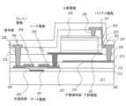
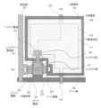
以下において、画素13のデバイス構造のいくつかの例を説明する。画素13に含まれる、フォトダイオード121、薄膜トランジスタ122及び容量素子126は、それぞれ、絶縁基板上で、積層構造を有している。
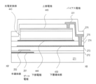
以下において、画素の他の構成例を説明する。図5Aは、画素13、ゲート線105及び信号線106の構造を模式的に示す平面図である。図5Bは、図5AのVB-VB´切断線における断面図を示し、図5Cは、図5AのVC-VC´切断線における断面図を示す。以下においては、図3Aから3Cを参照して説明した構成との相違点を主に説明する。
Claims (7)
- 基板上に配列された複数の素子を含む、フォトダイオードアレイであって、
前記複数の素子の各素子は、
上部電極と、
下部電極と、
前記上部電極と前記下部電極との間の光電変換部と、
前記下部電極より下層に位置する、下層導体部と、
前記下部電極と前記下層導体部との間の絶縁層と、
を含み、
前記フォトダイオードアレイは、
信号線と、
前記信号線と前記素子との導通の有無を切り替えるスイッチトランジスタと、
バイアス電極と、
前記バイアス電極及び前記下層導体部の前記スイッチトランジスタのチャネルの少なくとも一部を平面視において覆う部分を導通する、第1コンタクト部と、
前記バイアス電極及び前記上部電極を導通する、第2コンタクト部と、
を含み、
前記スイッチトランジスタは、前記下部電極より下層に位置するゲート電極を含み、
前記下層導体部の少なくとも一部は、平面視において前記下部電極の少なくとも一部と前記絶縁層を介して重なり、
前記下層導体部の一部は、前記スイッチトランジスタのチャネルの少なくとも一部を、平面視において覆う、
フォトダイオードアレイ。 - 請求項1に記載のフォトダイオードアレイであって、
前記複数の素子はマトリクス状にレイアウトされ、
前記下層導体部は、横方向及び縦方向において隣接する他の下層導体部と連結されている、
フォトダイオードアレイ。 - 請求項1に記載のフォトダイオードアレイであって、
前記スイッチトランジスタのソース/ドレイン電極と前記下層導体部は、同一絶縁層上に同一材料で構成されている、
フォトダイオードアレイ。 - 請求項1に記載のフォトダイオードアレイであって、
前記下層導体部は、平面視において前記下部電極と対向する領域に開口を有する、
フォトダイオードアレイ。 - 請求項1に記載のフォトダイオードアレイであって、
前記下層導体部の一部は、前記ゲート電極に信号を伝送するゲート線の少なくとも一部を、平面視において覆う、
フォトダイオードアレイ。 - 請求項5に記載のフォトダイオードアレイであって、
前記光電変換部の一部は、前記ゲート線の少なくとも一部を、平面視において覆う、
フォトダイオードアレイ。 - 請求項1に記載のフォトダイオードアレイと、
前記フォトダイオードアレイを駆動及び制御する回路と、
を含む、イメージセンサ。
Priority Applications (3)
| Application Number | Priority Date | Filing Date | Title |
|---|---|---|---|
| JP2021069804A JP7601696B2 (ja) | 2021-04-16 | 2021-04-16 | フォトダイオードアレイ及びイメージセンサ |
| CN202210362353.0A CN115224059A (zh) | 2021-04-16 | 2022-04-07 | 光电二极管阵列及图像传感器 |
| US17/721,180 US20220336517A1 (en) | 2021-04-16 | 2022-04-14 | Photodiode array and image sensor |
Applications Claiming Priority (1)
| Application Number | Priority Date | Filing Date | Title |
|---|---|---|---|
| JP2021069804A JP7601696B2 (ja) | 2021-04-16 | 2021-04-16 | フォトダイオードアレイ及びイメージセンサ |
Publications (3)
| Publication Number | Publication Date |
|---|---|
| JP2022164363A JP2022164363A (ja) | 2022-10-27 |
| JP2022164363A5 JP2022164363A5 (ja) | 2023-12-25 |
| JP7601696B2 true JP7601696B2 (ja) | 2024-12-17 |
Family
ID=83602807
Family Applications (1)
| Application Number | Title | Priority Date | Filing Date |
|---|---|---|---|
| JP2021069804A Active JP7601696B2 (ja) | 2021-04-16 | 2021-04-16 | フォトダイオードアレイ及びイメージセンサ |
Country Status (3)
| Country | Link |
|---|---|
| US (1) | US20220336517A1 (ja) |
| JP (1) | JP7601696B2 (ja) |
| CN (1) | CN115224059A (ja) |
Families Citing this family (2)
| Publication number | Priority date | Publication date | Assignee | Title |
|---|---|---|---|---|
| KR102862092B1 (ko) * | 2022-12-16 | 2025-09-22 | 포항공과대학교 산학협력단 | 시냅스 소자 및 그 구동 방법 |
| WO2026075082A1 (ja) * | 2024-10-02 | 2026-04-09 | 株式会社ジャパンディスプレイ | 検出装置 |
Citations (5)
| Publication number | Priority date | Publication date | Assignee | Title |
|---|---|---|---|---|
| JP2004265934A (ja) | 2003-02-14 | 2004-09-24 | Canon Inc | 固体撮像装置及び放射線撮像装置 |
| JP2007073724A (ja) | 2005-09-07 | 2007-03-22 | Hitachi Via Mechanics Ltd | キャパシタのトリミング方法及びプリント基板 |
| JP2009170646A (ja) | 2008-01-16 | 2009-07-30 | Nec Corp | キャパシタ、キャパシタ内蔵配線基板、及びその製造方法 |
| JP2009283896A (ja) | 2008-04-23 | 2009-12-03 | Epson Imaging Devices Corp | 固体撮像装置およびその製造方法 |
| JP2011249370A (ja) | 2010-05-21 | 2011-12-08 | Fujifilm Corp | 放射線検出器 |
Family Cites Families (10)
| Publication number | Priority date | Publication date | Assignee | Title |
|---|---|---|---|---|
| JP3018669B2 (ja) * | 1991-10-04 | 2000-03-13 | 富士ゼロックス株式会社 | 半導体センサ |
| US20160161426A1 (en) * | 2014-12-08 | 2016-06-09 | Zena Technologies, Inc. | Pillar Based Amorphous and Polycrystalline Photoconductors for X-ray Image Sensors |
| US8791419B2 (en) * | 2010-12-15 | 2014-07-29 | Carestream Health, Inc. | High charge capacity pixel architecture, photoelectric conversion apparatus, radiation image pickup system and methods for same |
| US9941324B2 (en) * | 2015-04-28 | 2018-04-10 | Nlt Technologies, Ltd. | Semiconductor device, method of manufacturing semiconductor device, photodiode array, and imaging apparatus |
| JP2017152656A (ja) * | 2016-02-26 | 2017-08-31 | Tianma Japan株式会社 | イメージセンサおよびその製造方法 |
| US9698193B1 (en) * | 2016-09-15 | 2017-07-04 | Ka Imaging Inc. | Multi-sensor pixel architecture for use in a digital imaging system |
| JP7308595B2 (ja) * | 2018-07-02 | 2023-07-14 | Tianma Japan株式会社 | イメージセンサ |
| US11251221B2 (en) * | 2018-09-06 | 2022-02-15 | Sharp Kabushiki Kaisha | Imaging panel and method for manufacturing same |
| JP7268986B2 (ja) * | 2018-10-05 | 2023-05-08 | Tianma Japan株式会社 | 整流性を有する素子と薄膜トランジスタとを含む装置 |
| CN112271186B (zh) * | 2019-07-08 | 2024-02-06 | 夏普株式会社 | 有源矩阵基板及其检查方法 |
-
2021
- 2021-04-16 JP JP2021069804A patent/JP7601696B2/ja active Active
-
2022
- 2022-04-07 CN CN202210362353.0A patent/CN115224059A/zh active Pending
- 2022-04-14 US US17/721,180 patent/US20220336517A1/en active Pending
Patent Citations (5)
| Publication number | Priority date | Publication date | Assignee | Title |
|---|---|---|---|---|
| JP2004265934A (ja) | 2003-02-14 | 2004-09-24 | Canon Inc | 固体撮像装置及び放射線撮像装置 |
| JP2007073724A (ja) | 2005-09-07 | 2007-03-22 | Hitachi Via Mechanics Ltd | キャパシタのトリミング方法及びプリント基板 |
| JP2009170646A (ja) | 2008-01-16 | 2009-07-30 | Nec Corp | キャパシタ、キャパシタ内蔵配線基板、及びその製造方法 |
| JP2009283896A (ja) | 2008-04-23 | 2009-12-03 | Epson Imaging Devices Corp | 固体撮像装置およびその製造方法 |
| JP2011249370A (ja) | 2010-05-21 | 2011-12-08 | Fujifilm Corp | 放射線検出器 |
Also Published As
| Publication number | Publication date |
|---|---|
| JP2022164363A (ja) | 2022-10-27 |
| CN115224059A (zh) | 2022-10-21 |
| US20220336517A1 (en) | 2022-10-20 |
Similar Documents
| Publication | Publication Date | Title |
|---|---|---|
| KR102642536B1 (ko) | 디지털 엑스레이 검출기용 기판, 이를 포함하는 디지털 엑스레이 검출기 및 제조 방법 | |
| CN109427837B (zh) | 用于数字x射线检测器的阵列基板及其制造方法 | |
| JP5080172B2 (ja) | 画像検出装置 | |
| EP1593160B1 (en) | Semiconductor radiation image pickup apparatus | |
| US9129871B2 (en) | Radioactive-ray imaging apparatus, radioactive-ray imaging display system and transistor | |
| KR102583562B1 (ko) | 디지털 엑스레이 검출기용 어레이 기판과 이를 포함하는 엑스레이 검출기 | |
| CN103066083B (zh) | 检测设备和检测系统 | |
| KR102522578B1 (ko) | 디지털 엑스레이 검출기용 어레이 기판과 이를 포함하는 디지털 엑스레이 검출기 | |
| JP2009087960A (ja) | センサパネル及び画像検出装置 | |
| JP7268986B2 (ja) | 整流性を有する素子と薄膜トランジスタとを含む装置 | |
| JP7601696B2 (ja) | フォトダイオードアレイ及びイメージセンサ | |
| EP2023163A2 (en) | Image detecion device | |
| KR20190079418A (ko) | 디지털 엑스레이 검출기 패널과 이를 포함하는 엑스레이 시스템 | |
| KR101628604B1 (ko) | 디지털 엑스레이 디텍터 | |
| US20110284749A1 (en) | Radiation detector | |
| JP4376522B2 (ja) | 電磁波検出器 | |
| JP5710904B2 (ja) | X線検出器 | |
| KR102670832B1 (ko) | 디지털 엑스레이 검출장치 | |
| JP2009272452A (ja) | 固体撮像装置 | |
| JP2009290171A (ja) | 固体撮像装置 | |
| US20230387151A1 (en) | Image sensor | |
| JP4357844B2 (ja) | 電磁波検出器 | |
| KR102631651B1 (ko) | 필팩터가 향상된 디지털 엑스레이 검출장치 | |
| US12550462B2 (en) | Imaging device | |
| KR20220047052A (ko) | 디지털 엑스레이 검출기용 박막 트랜지스터 어레이 기판과 이를 포함하는 디지털 엑스레이 검출기 |
Legal Events
| Date | Code | Title | Description |
|---|---|---|---|
| A521 | Request for written amendment filed |
Free format text: JAPANESE INTERMEDIATE CODE: A523 Effective date: 20231215 |
|
| A621 | Written request for application examination |
Free format text: JAPANESE INTERMEDIATE CODE: A621 Effective date: 20231215 |
|
| A977 | Report on retrieval |
Free format text: JAPANESE INTERMEDIATE CODE: A971007 Effective date: 20240725 |
|
| A131 | Notification of reasons for refusal |
Free format text: JAPANESE INTERMEDIATE CODE: A131 Effective date: 20240827 |
|
| A521 | Request for written amendment filed |
Free format text: JAPANESE INTERMEDIATE CODE: A523 Effective date: 20241021 |
|
| TRDD | Decision of grant or rejection written | ||
| A01 | Written decision to grant a patent or to grant a registration (utility model) |
Free format text: JAPANESE INTERMEDIATE CODE: A01 Effective date: 20241203 |
|
| A61 | First payment of annual fees (during grant procedure) |
Free format text: JAPANESE INTERMEDIATE CODE: A61 Effective date: 20241205 |
|
| R150 | Certificate of patent or registration of utility model |
Ref document number: 7601696 Country of ref document: JP Free format text: JAPANESE INTERMEDIATE CODE: R150 |