JP7610345B2 - 複合焼結体および複合焼結体の製造方法 - Google Patents
複合焼結体および複合焼結体の製造方法 Download PDFInfo
- Publication number
- JP7610345B2 JP7610345B2 JP2019197719A JP2019197719A JP7610345B2 JP 7610345 B2 JP7610345 B2 JP 7610345B2 JP 2019197719 A JP2019197719 A JP 2019197719A JP 2019197719 A JP2019197719 A JP 2019197719A JP 7610345 B2 JP7610345 B2 JP 7610345B2
- Authority
- JP
- Japan
- Prior art keywords
- electrode
- sintered body
- less
- titanium nitride
- tin
- Prior art date
- Legal status (The legal status is an assumption and is not a legal conclusion. Google has not performed a legal analysis and makes no representation as to the accuracy of the status listed.)
- Active
Links
Images


Classifications
-
- H—ELECTRICITY
- H10—SEMICONDUCTOR DEVICES; ELECTRIC SOLID-STATE DEVICES NOT OTHERWISE PROVIDED FOR
- H10P—GENERIC PROCESSES OR APPARATUS FOR THE MANUFACTURE OR TREATMENT OF DEVICES COVERED BY CLASS H10
- H10P72/00—Handling or holding of wafers, substrates or devices during manufacture or treatment thereof
- H10P72/70—Handling or holding of wafers, substrates or devices during manufacture or treatment thereof for supporting or gripping
- H10P72/72—Handling or holding of wafers, substrates or devices during manufacture or treatment thereof for supporting or gripping using electrostatic chucks
- H10P72/722—Details of electrostatic chucks
-
- H—ELECTRICITY
- H05—ELECTRIC TECHNIQUES NOT OTHERWISE PROVIDED FOR
- H05B—ELECTRIC HEATING; ELECTRIC LIGHT SOURCES NOT OTHERWISE PROVIDED FOR; CIRCUIT ARRANGEMENTS FOR ELECTRIC LIGHT SOURCES, IN GENERAL
- H05B3/00—Ohmic-resistance heating
- H05B3/10—Heating elements characterised by the composition or nature of the materials or by the arrangement of the conductor
- H05B3/12—Heating elements characterised by the composition or nature of the materials or by the arrangement of the conductor characterised by the composition or nature of the conductive material
-
- H—ELECTRICITY
- H10—SEMICONDUCTOR DEVICES; ELECTRIC SOLID-STATE DEVICES NOT OTHERWISE PROVIDED FOR
- H10D—INORGANIC ELECTRIC SEMICONDUCTOR DEVICES
- H10D48/00—Individual devices not covered by groups H10D1/00 - H10D44/00
- H10D48/01—Manufacture or treatment
- H10D48/04—Manufacture or treatment of devices having bodies comprising selenium or tellurium in uncombined form
- H10D48/042—Preparation of foundation plates
-
- H—ELECTRICITY
- H01—ELECTRIC ELEMENTS
- H01B—CABLES; CONDUCTORS; INSULATORS; SELECTION OF MATERIALS FOR THEIR CONDUCTIVE, INSULATING OR DIELECTRIC PROPERTIES
- H01B1/00—Conductors or conductive bodies characterised by the conductive materials; Selection of materials as conductors
- H01B1/02—Conductors or conductive bodies characterised by the conductive materials; Selection of materials as conductors mainly consisting of metals or alloys
-
- H—ELECTRICITY
- H05—ELECTRIC TECHNIQUES NOT OTHERWISE PROVIDED FOR
- H05B—ELECTRIC HEATING; ELECTRIC LIGHT SOURCES NOT OTHERWISE PROVIDED FOR; CIRCUIT ARRANGEMENTS FOR ELECTRIC LIGHT SOURCES, IN GENERAL
- H05B1/00—Details of electric heating devices
- H05B1/02—Automatic switching arrangements specially adapted to apparatus ; Control of heating devices
- H05B1/0227—Applications
- H05B1/023—Industrial applications
- H05B1/0233—Industrial applications for semiconductors manufacturing
-
- H—ELECTRICITY
- H05—ELECTRIC TECHNIQUES NOT OTHERWISE PROVIDED FOR
- H05B—ELECTRIC HEATING; ELECTRIC LIGHT SOURCES NOT OTHERWISE PROVIDED FOR; CIRCUIT ARRANGEMENTS FOR ELECTRIC LIGHT SOURCES, IN GENERAL
- H05B3/00—Ohmic-resistance heating
- H05B3/10—Heating elements characterised by the composition or nature of the materials or by the arrangement of the conductor
- H05B3/18—Heating elements characterised by the composition or nature of the materials or by the arrangement of the conductor the conductor being embedded in an insulating material
-
- H—ELECTRICITY
- H05—ELECTRIC TECHNIQUES NOT OTHERWISE PROVIDED FOR
- H05B—ELECTRIC HEATING; ELECTRIC LIGHT SOURCES NOT OTHERWISE PROVIDED FOR; CIRCUIT ARRANGEMENTS FOR ELECTRIC LIGHT SOURCES, IN GENERAL
- H05B3/00—Ohmic-resistance heating
- H05B3/20—Heating elements having extended surface area substantially in a two-dimensional [2D] plane, e.g. plate-heater
- H05B3/22—Heating elements having extended surface area substantially in a two-dimensional [2D] plane, e.g. plate-heater non-flexible
- H05B3/28—Heating elements having extended surface area substantially in a two-dimensional [2D] plane, e.g. plate-heater non-flexible heating conductor embedded in insulating material
- H05B3/283—Heating elements having extended surface area substantially in a two-dimensional [2D] plane, e.g. plate-heater non-flexible heating conductor embedded in insulating material the insulating material being an inorganic material, e.g. ceramic
-
- H—ELECTRICITY
- H05—ELECTRIC TECHNIQUES NOT OTHERWISE PROVIDED FOR
- H05B—ELECTRIC HEATING; ELECTRIC LIGHT SOURCES NOT OTHERWISE PROVIDED FOR; CIRCUIT ARRANGEMENTS FOR ELECTRIC LIGHT SOURCES, IN GENERAL
- H05B3/00—Ohmic-resistance heating
- H05B3/68—Heating arrangements specially adapted for cooking plates or analogous hot-plates
- H05B3/688—Fabrication of the plates
-
- H—ELECTRICITY
- H10—SEMICONDUCTOR DEVICES; ELECTRIC SOLID-STATE DEVICES NOT OTHERWISE PROVIDED FOR
- H10P—GENERIC PROCESSES OR APPARATUS FOR THE MANUFACTURE OR TREATMENT OF DEVICES COVERED BY CLASS H10
- H10P72/00—Handling or holding of wafers, substrates or devices during manufacture or treatment thereof
- H10P72/04—Apparatus for manufacture or treatment
- H10P72/0431—Apparatus for thermal treatment
- H10P72/0432—Apparatus for thermal treatment mainly by conduction
-
- H—ELECTRICITY
- H10—SEMICONDUCTOR DEVICES; ELECTRIC SOLID-STATE DEVICES NOT OTHERWISE PROVIDED FOR
- H10P—GENERIC PROCESSES OR APPARATUS FOR THE MANUFACTURE OR TREATMENT OF DEVICES COVERED BY CLASS H10
- H10P72/00—Handling or holding of wafers, substrates or devices during manufacture or treatment thereof
- H10P72/70—Handling or holding of wafers, substrates or devices during manufacture or treatment thereof for supporting or gripping
- H10P72/72—Handling or holding of wafers, substrates or devices during manufacture or treatment thereof for supporting or gripping using electrostatic chucks
-
- H—ELECTRICITY
- H10—SEMICONDUCTOR DEVICES; ELECTRIC SOLID-STATE DEVICES NOT OTHERWISE PROVIDED FOR
- H10P—GENERIC PROCESSES OR APPARATUS FOR THE MANUFACTURE OR TREATMENT OF DEVICES COVERED BY CLASS H10
- H10P72/00—Handling or holding of wafers, substrates or devices during manufacture or treatment thereof
- H10P72/70—Handling or holding of wafers, substrates or devices during manufacture or treatment thereof for supporting or gripping
- H10P72/76—Handling or holding of wafers, substrates or devices during manufacture or treatment thereof for supporting or gripping using mechanical means, e.g. clamps or pinches
- H10P72/7604—Handling or holding of wafers, substrates or devices during manufacture or treatment thereof for supporting or gripping using mechanical means, e.g. clamps or pinches the wafers being placed on a susceptor, stage or support
- H10P72/7616—Handling or holding of wafers, substrates or devices during manufacture or treatment thereof for supporting or gripping using mechanical means, e.g. clamps or pinches the wafers being placed on a susceptor, stage or support characterised by a coating, a hardness or a material
-
- H—ELECTRICITY
- H05—ELECTRIC TECHNIQUES NOT OTHERWISE PROVIDED FOR
- H05B—ELECTRIC HEATING; ELECTRIC LIGHT SOURCES NOT OTHERWISE PROVIDED FOR; CIRCUIT ARRANGEMENTS FOR ELECTRIC LIGHT SOURCES, IN GENERAL
- H05B2203/00—Aspects relating to Ohmic resistive heating covered by group H05B3/00
- H05B2203/002—Heaters using a particular layout for the resistive material or resistive elements
-
- H—ELECTRICITY
- H05—ELECTRIC TECHNIQUES NOT OTHERWISE PROVIDED FOR
- H05B—ELECTRIC HEATING; ELECTRIC LIGHT SOURCES NOT OTHERWISE PROVIDED FOR; CIRCUIT ARRANGEMENTS FOR ELECTRIC LIGHT SOURCES, IN GENERAL
- H05B2203/00—Aspects relating to Ohmic resistive heating covered by group H05B3/00
- H05B2203/013—Heaters using resistive films or coatings
-
- H—ELECTRICITY
- H05—ELECTRIC TECHNIQUES NOT OTHERWISE PROVIDED FOR
- H05B—ELECTRIC HEATING; ELECTRIC LIGHT SOURCES NOT OTHERWISE PROVIDED FOR; CIRCUIT ARRANGEMENTS FOR ELECTRIC LIGHT SOURCES, IN GENERAL
- H05B2203/00—Aspects relating to Ohmic resistive heating covered by group H05B3/00
- H05B2203/017—Manufacturing methods or apparatus for heaters
Landscapes
- Engineering & Computer Science (AREA)
- Manufacturing & Machinery (AREA)
- Chemical & Material Sciences (AREA)
- Ceramic Engineering (AREA)
- Inorganic Chemistry (AREA)
- Ceramic Products (AREA)
- Container, Conveyance, Adherence, Positioning, Of Wafer (AREA)
Description
好ましくは、前記電極に含まれる導電体における前記炭化タングステン(WC)および前記窒化チタン(TiN)の合計含有率は、100体積%である。
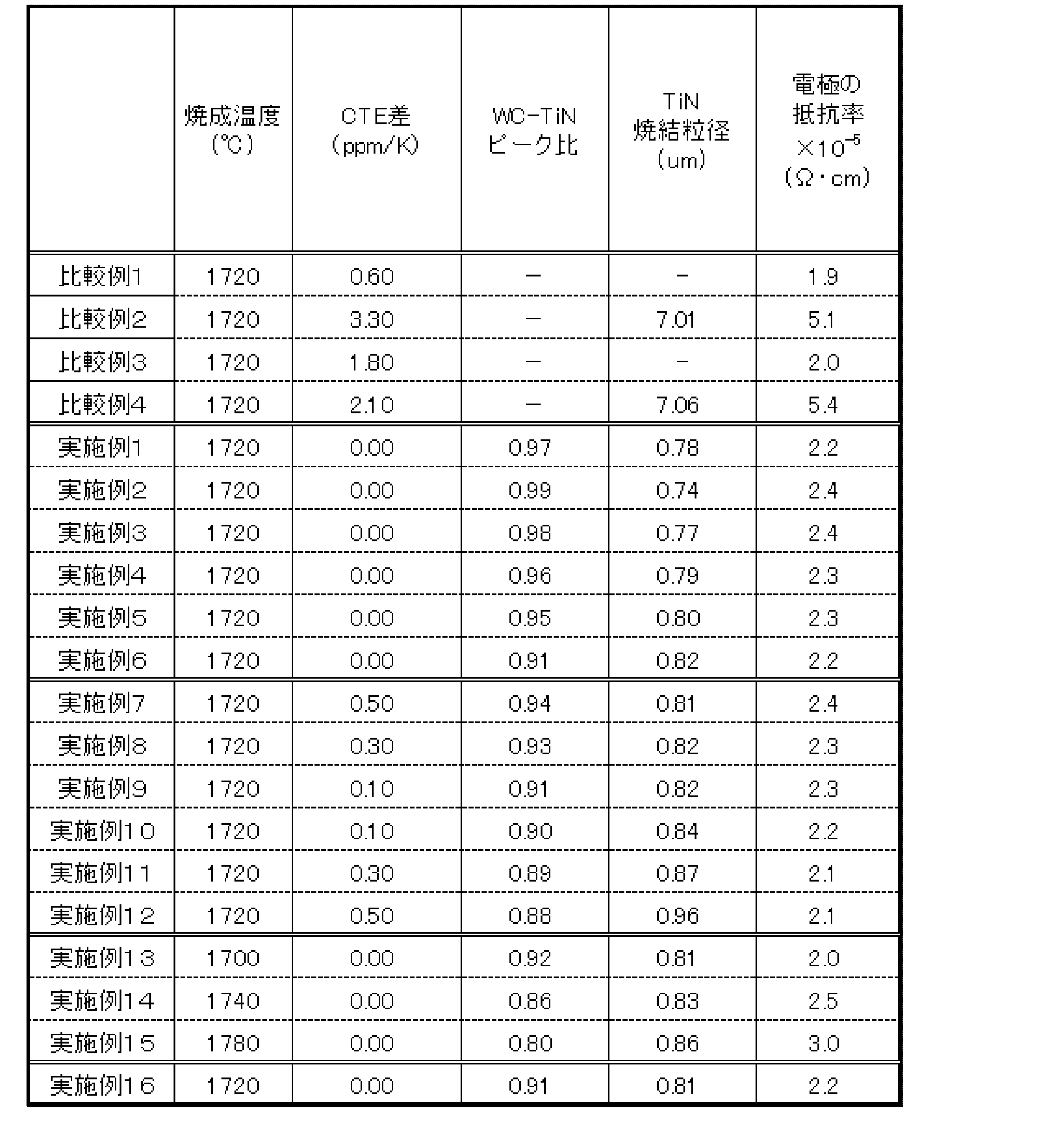
本発明の好ましい他の形態に係る複合焼結体は、50質量%~100質量%の窒化アルミニウムを含有するとともに主面に半導体基板が載置される円板状の基材と、前記基材の内部または表面に配置される電極と、を備える。前記電極は、炭化タングステン(WC)と、窒化チタン(TiN)と、を含む。前記電極に含まれる導電体における前記炭化タングステン(WC)および前記窒化チタン(TiN)の合計含有率は、100体積%である。前記電極と前記基材との熱膨張係数の差の絶対値は、40℃以上かつ1000℃以下の範囲において、0.3ppm/℃以下である。これにより、電極の抵抗率の増大を抑制しつつ、電極と基材との熱膨張係数の差を小さくすることができる。
好ましくは、前記電極における前記炭化タングステン(WC)および前記窒化チタン(TiN)の合計含有率は、100体積%である。
本発明の好ましい他の形態に係る複合焼結体の製造方法は、a)セラミックを主材料とする成形体、仮焼体または焼結体である第1部材および第2部材を準備する工程と、b)前記第1部材上に、炭化タングステン(WC)および窒化チタン(TiN)を含む電極または前記電極の前駆体を配置した後、前記第2部材を積層して積層体を形成する工程と、c)前記積層体をホットプレス焼成する工程と、を備える。前記c)工程の終了後における前記第1部材および前記第2部材は、50質量%~100質量%の窒化アルミニウムを含有する。前記c)工程の終了後において、前記電極に含まれる導電体における前記炭化タングステンおよび前記窒化チタンの合計含有率は、100体積%である。前記c)工程の終了後における前記電極と前記第1部材および前記第2部材との熱膨張係数の差の絶対値は、40℃以上かつ1000℃以下の範囲において、0.3ppm/℃以下である。これにより、電極の抵抗率の増大を抑制しつつ、電極と基材との熱膨張係数の差を小さくすることができる。


20 複合焼結体
21 本体部
23 電極
S11~S15 ステップ
Claims (11)
- 複合焼結体であって、
5質量%~45質量%のマグネシウムアルミニウムスピネルを含むとともに残部が窒化アルミニウムであり、主面に半導体基板が載置される円板状の基材と、
前記基材の内部または表面に配置される電極と、
を備え、
前記電極は、
炭化タングステンと、
窒化チタンと、
を含み、
前記電極と前記基材との熱膨張係数の差の絶対値は、40℃以上かつ1000℃以下の範囲において、0.3ppm/℃以下であることを特徴とする複合焼結体。 - 請求項1に記載の複合焼結体であって、
前記電極に含まれる導電体における前記炭化タングステンおよび前記窒化チタンの合計含有率は、100体積%であることを特徴とする複合焼結体。 - 複合焼結体であって、
50質量%~100質量%の窒化アルミニウムを含有するとともに主面に半導体基板が載置される円板状の基材と、
前記基材の内部または表面に配置される電極と、
を備え、
前記電極は、
炭化タングステンと、
窒化チタンと、
を含み、
前記電極に含まれる導電体における前記炭化タングステンおよび前記窒化チタンの合計含有率は、100体積%であり、
前記電極と前記基材との熱膨張係数の差の絶対値は、40℃以上かつ1000℃以下の範囲において、0.3ppm/℃以下であることを特徴とする複合焼結体。 - 請求項2または3に記載の複合焼結体であって、
前記電極における前記炭化タングステンおよび前記窒化チタンの合計含有率は、100体積%であることを特徴とする複合焼結体。 - 請求項1ないし4のいずれか1つに記載の複合焼結体であって、
前記電極の室温における抵抗率は、3.0×10⁻⁵Ω・cm以下であることを特徴とする複合焼結体。 - 請求項1ないし5のいずれか1つに記載の複合焼結体であって、
前記電極に含まれる導電体における前記窒化チタンの含有率は、5体積%以上かつ60体積%以下であることを特徴とする複合焼結体。 - 請求項1ないし6のいずれか1つに記載の複合焼結体であって、
前記電極において、X線回折法により得られる前記炭化タングステンと前記窒化チタンとのメインピークの強度比は、0.80以上かつ1.0未満であることを特徴とする複合焼結体。 - 請求項1ないし7のいずれか1つに記載の複合焼結体であって、
前記電極における前記窒化チタンの焼結粒径は、0.7μm以上かつ1.0μm以下であることを特徴とする複合焼結体。 - 主面に半導体基板が載置される円板状の基材および前記基材の内部に配置される電極を備える複合焼結体の製造方法であって、
a)セラミックを主材料とする成形体、仮焼体または焼結体である第1部材および第2部材を準備する工程と、
b)前記第1部材上に、炭化タングステンおよび窒化チタンを含む電極または前記電極の前駆体を配置した後、前記第2部材を積層して積層体を形成する工程と、
c)前記積層体をホットプレス焼成する工程と、
を備え、
前記c)工程の終了後における前記第1部材および前記第2部材は、5質量%~45質量%のマグネシウムアルミニウムスピネルを含むとともに残部が窒化アルミニウムであり、
前記c)工程の終了後における前記電極と前記第1部材および前記第2部材との熱膨張係数の差の絶対値は、40℃以上かつ1000℃以下の範囲において、0.3ppm/℃以下であることを特徴とする複合焼結体の製造方法。 - 主面に半導体基板が載置される円板状の基材および前記基材の内部に配置される電極を備える複合焼結体の製造方法であって、
a)セラミックを主材料とする成形体、仮焼体または焼結体である第1部材および第2部材を準備する工程と、
b)前記第1部材上に、炭化タングステンおよび窒化チタンを含む電極または前記電極の前駆体を配置した後、前記第2部材を積層して積層体を形成する工程と、
c)前記積層体をホットプレス焼成する工程と、
を備え、
前記c)工程の終了後における前記第1部材および前記第2部材は、50質量%~100質量%の窒化アルミニウムを含有し、
前記c)工程の終了後において、前記電極に含まれる導電体における前記炭化タングステンおよび前記窒化チタンの合計含有率は、100体積%であり、
前記c)工程の終了後における前記電極と前記第1部材および前記第2部材との熱膨張係数の差の絶対値は、40℃以上かつ1000℃以下の範囲において、0.3ppm/℃以下であることを特徴とする複合焼結体の製造方法。 - 請求項9または10に記載の複合焼結体の製造方法であって、
前記c)工程における焼成温度は、1700℃以上かつ1780℃以下であることを特徴とする複合焼結体の製造方法。
Priority Applications (7)
| Application Number | Priority Date | Filing Date | Title |
|---|---|---|---|
| JP2019197719A JP7610345B2 (ja) | 2019-10-30 | 2019-10-30 | 複合焼結体および複合焼結体の製造方法 |
| US17/070,149 US11715661B2 (en) | 2019-10-30 | 2020-10-14 | Composite sintered body and method of manufacturing composite sintered body |
| TW109135668A TWI764320B (zh) | 2019-10-30 | 2020-10-15 | 複合燒結體及複合燒結體的製造方法 |
| KR1020200134912A KR20210052250A (ko) | 2019-10-30 | 2020-10-19 | 복합 소결체 및 복합 소결체의 제조 방법 |
| CN202011160357.8A CN112750692B (zh) | 2019-10-30 | 2020-10-27 | 复合烧结体及复合烧结体的制造方法 |
| KR1020230033737A KR102737267B1 (ko) | 2019-10-30 | 2023-03-15 | 복합 소결체 및 복합 소결체의 제조 방법 |
| JP2024225110A JP2025028348A (ja) | 2019-10-30 | 2024-12-20 | 複合焼結体および複合焼結体の製造方法 |
Applications Claiming Priority (1)
| Application Number | Priority Date | Filing Date | Title |
|---|---|---|---|
| JP2019197719A JP7610345B2 (ja) | 2019-10-30 | 2019-10-30 | 複合焼結体および複合焼結体の製造方法 |
Related Child Applications (1)
| Application Number | Title | Priority Date | Filing Date |
|---|---|---|---|
| JP2024225110A Division JP2025028348A (ja) | 2019-10-30 | 2024-12-20 | 複合焼結体および複合焼結体の製造方法 |
Publications (2)
| Publication Number | Publication Date |
|---|---|
| JP2021072350A JP2021072350A (ja) | 2021-05-06 |
| JP7610345B2 true JP7610345B2 (ja) | 2025-01-08 |
Family
ID=75648731
Family Applications (2)
| Application Number | Title | Priority Date | Filing Date |
|---|---|---|---|
| JP2019197719A Active JP7610345B2 (ja) | 2019-10-30 | 2019-10-30 | 複合焼結体および複合焼結体の製造方法 |
| JP2024225110A Pending JP2025028348A (ja) | 2019-10-30 | 2024-12-20 | 複合焼結体および複合焼結体の製造方法 |
Family Applications After (1)
| Application Number | Title | Priority Date | Filing Date |
|---|---|---|---|
| JP2024225110A Pending JP2025028348A (ja) | 2019-10-30 | 2024-12-20 | 複合焼結体および複合焼結体の製造方法 |
Country Status (5)
| Country | Link |
|---|---|
| US (1) | US11715661B2 (ja) |
| JP (2) | JP7610345B2 (ja) |
| KR (2) | KR20210052250A (ja) |
| CN (1) | CN112750692B (ja) |
| TW (1) | TWI764320B (ja) |
Families Citing this family (1)
| Publication number | Priority date | Publication date | Assignee | Title |
|---|---|---|---|---|
| CN111868913B (zh) * | 2018-03-23 | 2023-08-22 | 住友大阪水泥股份有限公司 | 静电卡盘装置及静电卡盘装置的制造方法 |
Citations (7)
| Publication number | Priority date | Publication date | Assignee | Title |
|---|---|---|---|---|
| JP2006210390A (ja) | 2005-01-25 | 2006-08-10 | Taiheiyo Cement Corp | 静電チャックおよび露光装置 |
| JP2006270084A (ja) | 2005-02-24 | 2006-10-05 | Kyocera Corp | 静電チャックおよびウェハ保持部材並びにウェハ処理方法 |
| JP2007173592A (ja) | 2005-12-22 | 2007-07-05 | Kyocera Corp | 静電チャック |
| JP5032444B2 (ja) | 2007-11-14 | 2012-09-26 | 日本碍子株式会社 | 基板保持体 |
| WO2013054806A1 (ja) | 2011-10-11 | 2013-04-18 | 日本碍子株式会社 | セラミックス部材、半導体製造装置用部材及びセラミックス部材の製造方法 |
| JP2017157328A (ja) | 2016-02-29 | 2017-09-07 | 日本碍子株式会社 | セラミック構造体、その製法及び半導体製造装置用部材 |
| WO2018221504A1 (ja) | 2017-05-30 | 2018-12-06 | 京セラ株式会社 | 窒化アルミニウム質焼結体、および半導体保持装置 |
Family Cites Families (28)
| Publication number | Priority date | Publication date | Assignee | Title |
|---|---|---|---|---|
| JPS6060983A (ja) * | 1983-09-08 | 1985-04-08 | 株式会社デンソー | セラミックヒ−タ及びその製造方法 |
| JP2646083B2 (ja) * | 1986-11-27 | 1997-08-25 | 京セラ株式会社 | セラミツクヒータ |
| US4804823A (en) * | 1986-07-31 | 1989-02-14 | Kyocera Corporation | Ceramic heater |
| KR960016071B1 (ko) * | 1993-10-04 | 1996-11-27 | 한국과학기술연구원 | 판상세라믹 발열체 |
| JP2828575B2 (ja) * | 1993-11-12 | 1998-11-25 | 京セラ株式会社 | 窒化珪素質セラミックヒータ |
| US6133557A (en) | 1995-01-31 | 2000-10-17 | Kyocera Corporation | Wafer holding member |
| JPH08236599A (ja) * | 1995-02-28 | 1996-09-13 | Kyocera Corp | ウェハ保持装置 |
| JPH1025162A (ja) * | 1996-07-08 | 1998-01-27 | Kyocera Corp | セラミック焼結体 |
| JP3618032B2 (ja) * | 1997-02-17 | 2005-02-09 | 京セラ株式会社 | 静電チャック |
| JPH1161404A (ja) * | 1997-08-21 | 1999-03-05 | Hitachi Ltd | 静電吸着装置及びその製造方法並びにそれを用いた加工装置 |
| JP3323135B2 (ja) * | 1998-08-31 | 2002-09-09 | 京セラ株式会社 | 静電チャック |
| JP3963412B2 (ja) * | 1998-11-17 | 2007-08-22 | 日本特殊陶業株式会社 | セラミックヒータ用発熱抵抗体及びセラミックヒータ並びにセラミックヒータの製造方法 |
| JP2001297857A (ja) * | 1999-11-24 | 2001-10-26 | Ibiden Co Ltd | 半導体製造・検査装置用セラミックヒータ |
| EP1251551A1 (en) | 2000-08-30 | 2002-10-23 | Ibiden Co., Ltd. | Ceramic heater for semiconductor manufacturing and inspecting equipment |
| JP3758979B2 (ja) | 2001-02-27 | 2006-03-22 | 京セラ株式会社 | 静電チャック及び処理装置 |
| JP4043219B2 (ja) * | 2001-11-13 | 2008-02-06 | 株式会社日本セラテック | 静電チャック |
| CN1596557A (zh) | 2001-11-30 | 2005-03-16 | 揖斐电株式会社 | 陶瓷加热器 |
| JP3924524B2 (ja) * | 2002-10-29 | 2007-06-06 | 京セラ株式会社 | ウエハ加熱装置およびその製造方法 |
| JP4349952B2 (ja) * | 2004-03-24 | 2009-10-21 | 京セラ株式会社 | ウェハ支持部材とその製造方法 |
| JP4761723B2 (ja) | 2004-04-12 | 2011-08-31 | 日本碍子株式会社 | 基板加熱装置 |
| TW200612512A (en) * | 2004-06-28 | 2006-04-16 | Ngk Insulators Ltd | Substrate heating sapparatus |
| US20090159007A1 (en) | 2007-11-14 | 2009-06-25 | Ngk Insulators, Ltd. | Substrate support |
| KR20100096488A (ko) * | 2009-02-24 | 2010-09-02 | 삼성전자주식회사 | 리세스 채널 구조를 갖는 반도체 소자 |
| JP5505667B2 (ja) * | 2011-09-30 | 2014-05-28 | Toto株式会社 | 交流駆動静電チャック |
| JP6049509B2 (ja) | 2012-03-28 | 2016-12-21 | 日本碍子株式会社 | セラミックヒーター、ヒーター電極及びセラミックヒーターの製法 |
| WO2016042957A1 (ja) * | 2014-09-16 | 2016-03-24 | 日本碍子株式会社 | セラミック構造体、基板保持装置用部材及びセラミック構造体の製法 |
| JP7213710B2 (ja) * | 2018-03-23 | 2023-01-27 | 日本碍子株式会社 | 複合焼結体、半導体製造装置部材および複合焼結体の製造方法 |
| JP7465771B2 (ja) * | 2020-09-15 | 2024-04-11 | 日本碍子株式会社 | 複合焼結体、半導体製造装置部材および複合焼結体の製造方法 |
-
2019
- 2019-10-30 JP JP2019197719A patent/JP7610345B2/ja active Active
-
2020
- 2020-10-14 US US17/070,149 patent/US11715661B2/en active Active
- 2020-10-15 TW TW109135668A patent/TWI764320B/zh active
- 2020-10-19 KR KR1020200134912A patent/KR20210052250A/ko not_active Ceased
- 2020-10-27 CN CN202011160357.8A patent/CN112750692B/zh active Active
-
2023
- 2023-03-15 KR KR1020230033737A patent/KR102737267B1/ko active Active
-
2024
- 2024-12-20 JP JP2024225110A patent/JP2025028348A/ja active Pending
Patent Citations (7)
| Publication number | Priority date | Publication date | Assignee | Title |
|---|---|---|---|---|
| JP2006210390A (ja) | 2005-01-25 | 2006-08-10 | Taiheiyo Cement Corp | 静電チャックおよび露光装置 |
| JP2006270084A (ja) | 2005-02-24 | 2006-10-05 | Kyocera Corp | 静電チャックおよびウェハ保持部材並びにウェハ処理方法 |
| JP2007173592A (ja) | 2005-12-22 | 2007-07-05 | Kyocera Corp | 静電チャック |
| JP5032444B2 (ja) | 2007-11-14 | 2012-09-26 | 日本碍子株式会社 | 基板保持体 |
| WO2013054806A1 (ja) | 2011-10-11 | 2013-04-18 | 日本碍子株式会社 | セラミックス部材、半導体製造装置用部材及びセラミックス部材の製造方法 |
| JP2017157328A (ja) | 2016-02-29 | 2017-09-07 | 日本碍子株式会社 | セラミック構造体、その製法及び半導体製造装置用部材 |
| WO2018221504A1 (ja) | 2017-05-30 | 2018-12-06 | 京セラ株式会社 | 窒化アルミニウム質焼結体、および半導体保持装置 |
Also Published As
| Publication number | Publication date |
|---|---|
| KR20210052250A (ko) | 2021-05-10 |
| CN112750692B (zh) | 2024-03-08 |
| JP2021072350A (ja) | 2021-05-06 |
| US20210134639A1 (en) | 2021-05-06 |
| TWI764320B (zh) | 2022-05-11 |
| KR102737267B1 (ko) | 2024-12-03 |
| US11715661B2 (en) | 2023-08-01 |
| JP2025028348A (ja) | 2025-02-28 |
| TW202118746A (zh) | 2021-05-16 |
| CN112750692A (zh) | 2021-05-04 |
| KR20230042679A (ko) | 2023-03-29 |
Similar Documents
| Publication | Publication Date | Title |
|---|---|---|
| US9202718B2 (en) | Electrostatic chuck | |
| US11845697B2 (en) | Composite sintered body, semiconductor manufacturing apparatus member, and method of manufacturing composite sintered body | |
| JP7465771B2 (ja) | 複合焼結体、半導体製造装置部材および複合焼結体の製造方法 | |
| US10863587B2 (en) | Ceramic structure, method for manufacturing the same, and member for semiconductor manufacturing apparatus | |
| US12315757B2 (en) | Stacked structure and semiconductor manufacturing apparatus member | |
| JP2025028348A (ja) | 複合焼結体および複合焼結体の製造方法 | |
| JPWO2019163710A1 (ja) | 複合焼結体、半導体製造装置部材および複合焼結体の製造方法 | |
| JP7692293B2 (ja) | 複合焼結体、半導体製造装置部材および複合焼結体の製造方法 | |
| TWI864327B (zh) | 複合燒結體、半導體製造裝置部件及複合燒結體的製造方法 | |
| WO2025215770A1 (ja) | 半導体製造装置用ヒータ |
Legal Events
| Date | Code | Title | Description |
|---|---|---|---|
| A621 | Written request for application examination |
Free format text: JAPANESE INTERMEDIATE CODE: A621 Effective date: 20220722 |
|
| A131 | Notification of reasons for refusal |
Free format text: JAPANESE INTERMEDIATE CODE: A131 Effective date: 20230928 |
|
| A521 | Request for written amendment filed |
Free format text: JAPANESE INTERMEDIATE CODE: A523 Effective date: 20231115 |
|
| A131 | Notification of reasons for refusal |
Free format text: JAPANESE INTERMEDIATE CODE: A131 Effective date: 20240208 |
|
| A521 | Request for written amendment filed |
Free format text: JAPANESE INTERMEDIATE CODE: A523 Effective date: 20240312 |
|
| A131 | Notification of reasons for refusal |
Free format text: JAPANESE INTERMEDIATE CODE: A131 Effective date: 20240701 |
|
| A521 | Request for written amendment filed |
Free format text: JAPANESE INTERMEDIATE CODE: A523 Effective date: 20240808 |
|
| TRDD | Decision of grant or rejection written | ||
| A01 | Written decision to grant a patent or to grant a registration (utility model) |
Free format text: JAPANESE INTERMEDIATE CODE: A01 Effective date: 20241125 |
|
| A61 | First payment of annual fees (during grant procedure) |
Free format text: JAPANESE INTERMEDIATE CODE: A61 Effective date: 20241220 |
|
| R150 | Certificate of patent or registration of utility model |
Ref document number: 7610345 Country of ref document: JP Free format text: JAPANESE INTERMEDIATE CODE: R150 |