JP7614896B2 - 半導体装置及びその製造方法 - Google Patents
半導体装置及びその製造方法 Download PDFInfo
- Publication number
- JP7614896B2 JP7614896B2 JP2021045548A JP2021045548A JP7614896B2 JP 7614896 B2 JP7614896 B2 JP 7614896B2 JP 2021045548 A JP2021045548 A JP 2021045548A JP 2021045548 A JP2021045548 A JP 2021045548A JP 7614896 B2 JP7614896 B2 JP 7614896B2
- Authority
- JP
- Japan
- Prior art keywords
- electrode
- region
- substrate
- upper electrode
- semiconductor device
- Prior art date
- Legal status (The legal status is an assumption and is not a legal conclusion. Google has not performed a legal analysis and makes no representation as to the accuracy of the status listed.)
- Active
Links
Images



Classifications
-
- H—ELECTRICITY
- H10—SEMICONDUCTOR DEVICES; ELECTRIC SOLID-STATE DEVICES NOT OTHERWISE PROVIDED FOR
- H10D—INORGANIC ELECTRIC SEMICONDUCTOR DEVICES
- H10D30/00—Field-effect transistors [FET]
- H10D30/60—Insulated-gate field-effect transistors [IGFET]
- H10D30/63—Vertical IGFETs
-
- H—ELECTRICITY
- H10—SEMICONDUCTOR DEVICES; ELECTRIC SOLID-STATE DEVICES NOT OTHERWISE PROVIDED FOR
- H10D—INORGANIC ELECTRIC SEMICONDUCTOR DEVICES
- H10D30/00—Field-effect transistors [FET]
- H10D30/60—Insulated-gate field-effect transistors [IGFET]
- H10D30/64—Double-diffused metal-oxide semiconductor [DMOS] FETs
- H10D30/66—Vertical DMOS [VDMOS] FETs
- H10D30/668—Vertical DMOS [VDMOS] FETs having trench gate electrodes, e.g. UMOS transistors
-
- H—ELECTRICITY
- H10—SEMICONDUCTOR DEVICES; ELECTRIC SOLID-STATE DEVICES NOT OTHERWISE PROVIDED FOR
- H10D—INORGANIC ELECTRIC SEMICONDUCTOR DEVICES
- H10D30/00—Field-effect transistors [FET]
- H10D30/01—Manufacture or treatment
- H10D30/021—Manufacture or treatment of FETs having insulated gates [IGFET]
- H10D30/025—Manufacture or treatment of FETs having insulated gates [IGFET] of vertical IGFETs
-
- H—ELECTRICITY
- H10—SEMICONDUCTOR DEVICES; ELECTRIC SOLID-STATE DEVICES NOT OTHERWISE PROVIDED FOR
- H10D—INORGANIC ELECTRIC SEMICONDUCTOR DEVICES
- H10D30/00—Field-effect transistors [FET]
- H10D30/01—Manufacture or treatment
- H10D30/021—Manufacture or treatment of FETs having insulated gates [IGFET]
- H10D30/028—Manufacture or treatment of FETs having insulated gates [IGFET] of double-diffused metal oxide semiconductor [DMOS] FETs
- H10D30/0291—Manufacture or treatment of FETs having insulated gates [IGFET] of double-diffused metal oxide semiconductor [DMOS] FETs of vertical DMOS [VDMOS] FETs
- H10D30/0297—Manufacture or treatment of FETs having insulated gates [IGFET] of double-diffused metal oxide semiconductor [DMOS] FETs of vertical DMOS [VDMOS] FETs using recessing of the gate electrodes, e.g. to form trench gate electrodes
-
- H—ELECTRICITY
- H10—SEMICONDUCTOR DEVICES; ELECTRIC SOLID-STATE DEVICES NOT OTHERWISE PROVIDED FOR
- H10D—INORGANIC ELECTRIC SEMICONDUCTOR DEVICES
- H10D62/00—Semiconductor bodies, or regions thereof, of devices having potential barriers
- H10D62/10—Shapes, relative sizes or dispositions of the regions of the semiconductor bodies; Shapes of the semiconductor bodies
- H10D62/13—Semiconductor regions connected to electrodes carrying current to be rectified, amplified or switched, e.g. source or drain regions
- H10D62/149—Source or drain regions of field-effect devices
- H10D62/151—Source or drain regions of field-effect devices of IGFETs
- H10D62/156—Drain regions of DMOS transistors
-
- H—ELECTRICITY
- H10—SEMICONDUCTOR DEVICES; ELECTRIC SOLID-STATE DEVICES NOT OTHERWISE PROVIDED FOR
- H10D—INORGANIC ELECTRIC SEMICONDUCTOR DEVICES
- H10D62/00—Semiconductor bodies, or regions thereof, of devices having potential barriers
- H10D62/50—Physical imperfections
- H10D62/53—Physical imperfections the imperfections being within the semiconductor body
-
- H—ELECTRICITY
- H10—SEMICONDUCTOR DEVICES; ELECTRIC SOLID-STATE DEVICES NOT OTHERWISE PROVIDED FOR
- H10D—INORGANIC ELECTRIC SEMICONDUCTOR DEVICES
- H10D64/00—Electrodes of devices having potential barriers
- H10D64/111—Field plates
- H10D64/117—Recessed field plates, e.g. trench field plates or buried field plates
-
- H—ELECTRICITY
- H10—SEMICONDUCTOR DEVICES; ELECTRIC SOLID-STATE DEVICES NOT OTHERWISE PROVIDED FOR
- H10D—INORGANIC ELECTRIC SEMICONDUCTOR DEVICES
- H10D64/00—Electrodes of devices having potential barriers
- H10D64/20—Electrodes characterised by their shapes, relative sizes or dispositions
- H10D64/27—Electrodes not carrying the current to be rectified, amplified, oscillated or switched, e.g. gates
- H10D64/311—Gate electrodes for field-effect devices
- H10D64/411—Gate electrodes for field-effect devices for FETs
- H10D64/511—Gate electrodes for field-effect devices for FETs for IGFETs
- H10D64/512—Disposition of the gate electrodes, e.g. buried gates
- H10D64/513—Disposition of the gate electrodes, e.g. buried gates within recesses in the substrate, e.g. trench gates, groove gates or buried gates
-
- H—ELECTRICITY
- H10—SEMICONDUCTOR DEVICES; ELECTRIC SOLID-STATE DEVICES NOT OTHERWISE PROVIDED FOR
- H10D—INORGANIC ELECTRIC SEMICONDUCTOR DEVICES
- H10D84/00—Integrated devices formed in or on semiconductor substrates that comprise only semiconducting layers, e.g. on Si wafers or on GaAs-on-Si wafers
- H10D84/101—Integrated devices comprising main components and built-in components, e.g. IGBT having built-in freewheel diode
- H10D84/141—VDMOS having built-in components
-
- H—ELECTRICITY
- H10—SEMICONDUCTOR DEVICES; ELECTRIC SOLID-STATE DEVICES NOT OTHERWISE PROVIDED FOR
- H10D—INORGANIC ELECTRIC SEMICONDUCTOR DEVICES
- H10D84/00—Integrated devices formed in or on semiconductor substrates that comprise only semiconducting layers, e.g. on Si wafers or on GaAs-on-Si wafers
- H10D84/80—Integrated devices formed in or on semiconductor substrates that comprise only semiconducting layers, e.g. on Si wafers or on GaAs-on-Si wafers characterised by the integration of at least one component covered by groups H10D12/00 or H10D30/00, e.g. integration of IGFETs
- H10D84/811—Combinations of field-effect devices and one or more diodes, capacitors or resistors
-
- H—ELECTRICITY
- H10—SEMICONDUCTOR DEVICES; ELECTRIC SOLID-STATE DEVICES NOT OTHERWISE PROVIDED FOR
- H10P—GENERIC PROCESSES OR APPARATUS FOR THE MANUFACTURE OR TREATMENT OF DEVICES COVERED BY CLASS H10
- H10P34/00—Irradiation with electromagnetic or particle radiation of wafers, substrates or parts of devices
- H10P34/40—Irradiation with electromagnetic or particle radiation of wafers, substrates or parts of devices with high-energy radiation
-
- H—ELECTRICITY
- H10—SEMICONDUCTOR DEVICES; ELECTRIC SOLID-STATE DEVICES NOT OTHERWISE PROVIDED FOR
- H10D—INORGANIC ELECTRIC SEMICONDUCTOR DEVICES
- H10D64/00—Electrodes of devices having potential barriers
- H10D64/20—Electrodes characterised by their shapes, relative sizes or dispositions
-
- H—ELECTRICITY
- H10—SEMICONDUCTOR DEVICES; ELECTRIC SOLID-STATE DEVICES NOT OTHERWISE PROVIDED FOR
- H10D—INORGANIC ELECTRIC SEMICONDUCTOR DEVICES
- H10D64/00—Electrodes of devices having potential barriers
- H10D64/20—Electrodes characterised by their shapes, relative sizes or dispositions
- H10D64/27—Electrodes not carrying the current to be rectified, amplified, oscillated or switched, e.g. gates
- H10D64/311—Gate electrodes for field-effect devices
- H10D64/411—Gate electrodes for field-effect devices for FETs
- H10D64/511—Gate electrodes for field-effect devices for FETs for IGFETs
- H10D64/517—Gate electrodes for field-effect devices for FETs for IGFETs characterised by the conducting layers
- H10D64/518—Gate electrodes for field-effect devices for FETs for IGFETs characterised by the conducting layers characterised by their lengths or sectional shapes
Landscapes
- Electrodes Of Semiconductors (AREA)
Description
Claims (6)
- 上部電極と、
下部電極と、
前記上部電極と前記下部電極との間に位置するn型の基板と、
前記基板と前記上部電極との間に位置し、ゲート電極を有する埋め込み電極部と、
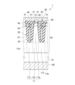
前記基板と前記上部電極との間に位置し、前記基板に接するn型のドリフト層を有するシリコン層であって、前記埋め込み電極部に隣接し、前記ドリフト層の一部と、前記ドリフト層の前記一部上に設けられたp型のベース層とを含むメサ部と、前記メサ部と前記基板との間に位置し、前記ドリフト層に含まれ、前記ベース層から離れて位置し、下端が前記基板と接する又は前記基板よりも上方に位置する第1領域と、前記埋め込み電極部と前記基板との間に位置し、前記ドリフト層に含まれる第2領域とを有し、前記第1領域と前記第2領域とは、前記埋め込み電極部と前記メサ部とが隣接する方向において連続し、前記ドリフト層の結晶欠陥密度のピークは前記第1領域にある、シリコン層と、
を備える半導体装置。 - 前記第1領域の水素濃度は、前記第2領域の水素濃度よりも高い請求項1に記載の半導体装置。
- 前記第2領域に結晶欠陥がない請求項1または2に記載の半導体装置。
- 前記第1領域と前記上部電極との間に、前記埋め込み電極部が位置しない請求項1~3のいずれか1つに記載の半導体装置。
- 基板上に、ゲート電極を有する埋め込み電極部と、前記埋め込み電極部に隣接するメサ部とを有するシリコン層とを形成する工程と、
前記メサ部の上に位置する第1部分と、前記埋め込み電極部の上に位置し、前記第1部分よりも厚い第2部分とを有する上部電極を前記埋め込み電極の上及び前記シリコン層の上に形成する工程と、
前記上部電極をマスクにして、前記上部電極側からエネルギー粒子を照射して、前記シリコン層における前記メサ部の下の領域に前記エネルギー粒子を到達させる工程と、
備える半導体装置の製造方法。 - 前記エネルギー粒子は、プロトンまたは電子である請求項5に記載の半導体装置の製造方法。
Priority Applications (3)
| Application Number | Priority Date | Filing Date | Title |
|---|---|---|---|
| JP2021045548A JP7614896B2 (ja) | 2021-03-19 | 2021-03-19 | 半導体装置及びその製造方法 |
| CN202110861191.0A CN115117168B (zh) | 2021-03-19 | 2021-07-29 | 半导体装置及其制造方法 |
| US17/470,626 US11869970B2 (en) | 2021-03-19 | 2021-09-09 | Semiconductor device including energy level in drift layer |
Applications Claiming Priority (1)
| Application Number | Priority Date | Filing Date | Title |
|---|---|---|---|
| JP2021045548A JP7614896B2 (ja) | 2021-03-19 | 2021-03-19 | 半導体装置及びその製造方法 |
Publications (2)
| Publication Number | Publication Date |
|---|---|
| JP2022144504A JP2022144504A (ja) | 2022-10-03 |
| JP7614896B2 true JP7614896B2 (ja) | 2025-01-16 |
Family
ID=83284327
Family Applications (1)
| Application Number | Title | Priority Date | Filing Date |
|---|---|---|---|
| JP2021045548A Active JP7614896B2 (ja) | 2021-03-19 | 2021-03-19 | 半導体装置及びその製造方法 |
Country Status (3)
| Country | Link |
|---|---|
| US (1) | US11869970B2 (ja) |
| JP (1) | JP7614896B2 (ja) |
| CN (1) | CN115117168B (ja) |
Citations (4)
| Publication number | Priority date | Publication date | Assignee | Title |
|---|---|---|---|---|
| WO2018110703A1 (ja) | 2016-12-16 | 2018-06-21 | 富士電機株式会社 | 半導体装置および製造方法 |
| WO2020036015A1 (ja) | 2018-08-14 | 2020-02-20 | 富士電機株式会社 | 半導体装置および製造方法 |
| JP2020072137A (ja) | 2018-10-30 | 2020-05-07 | 三菱電機株式会社 | 半導体装置 |
| US20200203513A1 (en) | 2018-12-21 | 2020-06-25 | Infineon Technologies Ag | Semiconductor device including silicon carbide body and method of manufacturing |
Family Cites Families (16)
| Publication number | Priority date | Publication date | Assignee | Title |
|---|---|---|---|---|
| JP2004133698A (ja) | 2002-10-10 | 2004-04-30 | Dainippon Printing Co Ltd | 印刷物に対する2次情報を提供する方法及びサーバ |
| DE102007036147B4 (de) * | 2007-08-02 | 2017-12-21 | Infineon Technologies Austria Ag | Verfahren zum Herstellen eines Halbleiterkörpers mit einer Rekombinationszone |
| JP5418067B2 (ja) | 2009-08-25 | 2014-02-19 | トヨタ自動車株式会社 | 絶縁ゲート型半導体装置 |
| JP5499692B2 (ja) * | 2009-12-24 | 2014-05-21 | トヨタ自動車株式会社 | 半導体装置及びその製造方法 |
| US7977742B1 (en) * | 2010-08-20 | 2011-07-12 | Monolithic Power Systems, Inc. | Trench-gate MOSFET with capacitively depleted drift region |
| CN103125023B (zh) * | 2011-09-28 | 2016-05-25 | 丰田自动车株式会社 | 半导体装置及其制造方法 |
| JP5291784B2 (ja) | 2011-11-18 | 2013-09-18 | 三菱重工業株式会社 | 橋梁の設計方法 |
| US8558308B1 (en) | 2012-06-14 | 2013-10-15 | Infineon Technologies Austria Ag | Method of manufacturing a semiconductor device using a contact implant and a metallic recombination element and semiconductor |
| JP6107767B2 (ja) | 2013-12-27 | 2017-04-05 | トヨタ自動車株式会社 | 半導体装置とその製造方法 |
| JP6665713B2 (ja) | 2016-06-28 | 2020-03-13 | トヨタ自動車株式会社 | 半導体装置 |
| JP6780335B2 (ja) | 2016-07-15 | 2020-11-04 | 富士電機株式会社 | 逆阻止mos型半導体装置および逆阻止mos型半導体装置の製造方法 |
| JP6666292B2 (ja) * | 2017-03-22 | 2020-03-13 | トヨタ自動車株式会社 | 半導体装置 |
| JP6816624B2 (ja) | 2017-04-13 | 2021-01-20 | 株式会社デンソー | 半導体装置の製造方法 |
| JP7102948B2 (ja) * | 2017-10-26 | 2022-07-20 | 株式会社デンソー | 炭化珪素半導体装置およびその製造方法 |
| WO2019083017A1 (ja) * | 2017-10-26 | 2019-05-02 | 株式会社デンソー | 炭化珪素半導体装置およびその製造方法 |
| JP7003688B2 (ja) | 2018-01-25 | 2022-01-20 | 株式会社デンソー | 半導体装置及びその製造方法 |
-
2021
- 2021-03-19 JP JP2021045548A patent/JP7614896B2/ja active Active
- 2021-07-29 CN CN202110861191.0A patent/CN115117168B/zh active Active
- 2021-09-09 US US17/470,626 patent/US11869970B2/en active Active
Patent Citations (4)
| Publication number | Priority date | Publication date | Assignee | Title |
|---|---|---|---|---|
| WO2018110703A1 (ja) | 2016-12-16 | 2018-06-21 | 富士電機株式会社 | 半導体装置および製造方法 |
| WO2020036015A1 (ja) | 2018-08-14 | 2020-02-20 | 富士電機株式会社 | 半導体装置および製造方法 |
| JP2020072137A (ja) | 2018-10-30 | 2020-05-07 | 三菱電機株式会社 | 半導体装置 |
| US20200203513A1 (en) | 2018-12-21 | 2020-06-25 | Infineon Technologies Ag | Semiconductor device including silicon carbide body and method of manufacturing |
Also Published As
| Publication number | Publication date |
|---|---|
| US11869970B2 (en) | 2024-01-09 |
| CN115117168A (zh) | 2022-09-27 |
| US20220302307A1 (en) | 2022-09-22 |
| JP2022144504A (ja) | 2022-10-03 |
| CN115117168B (zh) | 2026-04-03 |
Similar Documents
| Publication | Publication Date | Title |
|---|---|---|
| JP6724993B2 (ja) | 半導体装置および半導体装置の製造方法 | |
| US11901443B2 (en) | Semiconductor device and manufacturing method | |
| CN102376759B (zh) | 具有igbt区和二极管区的半导体装置 | |
| US10468510B2 (en) | Semiconductor device and manufacturing method of the same | |
| US20210013310A1 (en) | Silicon Carbide Device with Compensation Layer and Method of Manufacturing | |
| JP5519226B2 (ja) | ロバスト半導体デバイス | |
| US9397206B2 (en) | Semiconductor device and method for manufacturing the same | |
| US10903202B2 (en) | Semiconductor device | |
| US11158630B2 (en) | Semiconductor device | |
| JP6880669B2 (ja) | 炭化珪素半導体装置および炭化珪素半導体装置の製造方法 | |
| US20170263757A1 (en) | Silicon carbide semiconductor device and method for manufacturing same | |
| US20210126092A1 (en) | Semiconductor device and method of manufacturing semiconductor device | |
| US11183601B2 (en) | Semiconductor device with carrier lifetime control | |
| JP6988175B2 (ja) | 炭化珪素半導体装置および炭化珪素半導体装置の製造方法 | |
| US9048095B2 (en) | Method for manufacturing a semiconductor device having a channel region in a trench | |
| CN114600251B (zh) | 碳化硅半导体装置及其制造方法 | |
| KR20160012879A (ko) | 반도체 장치 | |
| JPWO2013161116A1 (ja) | 半導体装置及びその製造方法 | |
| WO2020075248A1 (ja) | 半導体装置及びその製造方法 | |
| JPWO2014087543A1 (ja) | 半導体装置の製造方法 | |
| JP5043445B2 (ja) | 半導体デバイスの製造方法 | |
| JP2008263217A (ja) | 半導体装置 | |
| JP2018006420A (ja) | 半導体装置 | |
| JP7156425B2 (ja) | 半導体装置 | |
| CN115117168B (zh) | 半导体装置及其制造方法 |
Legal Events
| Date | Code | Title | Description |
|---|---|---|---|
| A621 | Written request for application examination |
Free format text: JAPANESE INTERMEDIATE CODE: A621 Effective date: 20230202 |
|
| RD01 | Notification of change of attorney |
Free format text: JAPANESE INTERMEDIATE CODE: A7421 Effective date: 20230623 |
|
| A977 | Report on retrieval |
Free format text: JAPANESE INTERMEDIATE CODE: A971007 Effective date: 20231128 |
|
| A131 | Notification of reasons for refusal |
Free format text: JAPANESE INTERMEDIATE CODE: A131 Effective date: 20231220 |
|
| A521 | Request for written amendment filed |
Free format text: JAPANESE INTERMEDIATE CODE: A523 Effective date: 20240215 |
|
| A02 | Decision of refusal |
Free format text: JAPANESE INTERMEDIATE CODE: A02 Effective date: 20240604 |
|
| A521 | Request for written amendment filed |
Free format text: JAPANESE INTERMEDIATE CODE: A523 Effective date: 20240826 |
|
| A911 | Transfer to examiner for re-examination before appeal (zenchi) |
Free format text: JAPANESE INTERMEDIATE CODE: A911 Effective date: 20240903 |
|
| TRDD | Decision of grant or rejection written | ||
| A01 | Written decision to grant a patent or to grant a registration (utility model) |
Free format text: JAPANESE INTERMEDIATE CODE: A01 Effective date: 20241202 |
|
| A61 | First payment of annual fees (during grant procedure) |
Free format text: JAPANESE INTERMEDIATE CODE: A61 Effective date: 20241227 |
|
| R150 | Certificate of patent or registration of utility model |
Ref document number: 7614896 Country of ref document: JP Free format text: JAPANESE INTERMEDIATE CODE: R150 |