JP7617735B2 - 測定ユニット - Google Patents
測定ユニット Download PDFInfo
- Publication number
- JP7617735B2 JP7617735B2 JP2020209745A JP2020209745A JP7617735B2 JP 7617735 B2 JP7617735 B2 JP 7617735B2 JP 2020209745 A JP2020209745 A JP 2020209745A JP 2020209745 A JP2020209745 A JP 2020209745A JP 7617735 B2 JP7617735 B2 JP 7617735B2
- Authority
- JP
- Japan
- Prior art keywords
- ground
- signal
- dielectric
- conductor
- ground plate
- Prior art date
- Legal status (The legal status is an assumption and is not a legal conclusion. Google has not performed a legal analysis and makes no representation as to the accuracy of the status listed.)
- Active
Links
- 238000005259 measurement Methods 0.000 title claims description 39
- 239000004020 conductor Substances 0.000 claims description 173
- 239000000523 sample Substances 0.000 claims description 86
- 239000003989 dielectric material Substances 0.000 claims 1
- 238000012986 modification Methods 0.000 description 29
- 230000004048 modification Effects 0.000 description 29
- 238000010586 diagram Methods 0.000 description 18
- PXHVJJICTQNCMI-UHFFFAOYSA-N Nickel Chemical compound [Ni] PXHVJJICTQNCMI-UHFFFAOYSA-N 0.000 description 8
- 238000005476 soldering Methods 0.000 description 6
- RYGMFSIKBFXOCR-UHFFFAOYSA-N Copper Chemical compound [Cu] RYGMFSIKBFXOCR-UHFFFAOYSA-N 0.000 description 4
- 238000007796 conventional method Methods 0.000 description 4
- 229910052802 copper Inorganic materials 0.000 description 4
- 239000010949 copper Substances 0.000 description 4
- 229910052759 nickel Inorganic materials 0.000 description 4
- 229910001220 stainless steel Inorganic materials 0.000 description 4
- 239000010935 stainless steel Substances 0.000 description 4
- 239000000463 material Substances 0.000 description 3
- 238000007689 inspection Methods 0.000 description 2
- 230000005540 biological transmission Effects 0.000 description 1
- 239000000919 ceramic Substances 0.000 description 1
- 238000013461 design Methods 0.000 description 1
- 239000011810 insulating material Substances 0.000 description 1
- 239000004973 liquid crystal related substance Substances 0.000 description 1
- 238000004519 manufacturing process Methods 0.000 description 1
- 238000003825 pressing Methods 0.000 description 1
- 239000011347 resin Substances 0.000 description 1
- 229920005989 resin Polymers 0.000 description 1
- 239000004065 semiconductor Substances 0.000 description 1
- 229910052710 silicon Inorganic materials 0.000 description 1
- 239000010703 silicon Substances 0.000 description 1
- 239000007787 solid Substances 0.000 description 1
- 238000012360 testing method Methods 0.000 description 1
Images




Classifications
-
- G—PHYSICS
- G01—MEASURING; TESTING
- G01R—MEASURING ELECTRIC VARIABLES; MEASURING MAGNETIC VARIABLES
- G01R1/00—Details of instruments or arrangements of the types included in groups G01R5/00 - G01R13/00 and G01R31/00
- G01R1/02—General constructional details
- G01R1/04—Housings; Supporting members; Arrangements of terminals
- G01R1/0408—Test fixtures or contact fields; Connectors or connecting adaptors; Test clips; Test sockets
- G01R1/0416—Connectors, terminals
-
- G—PHYSICS
- G01—MEASURING; TESTING
- G01R—MEASURING ELECTRIC VARIABLES; MEASURING MAGNETIC VARIABLES
- G01R31/00—Arrangements for testing electric properties; Arrangements for locating electric faults; Arrangements for electrical testing characterised by what is being tested not provided for elsewhere
- G01R31/50—Testing of electric apparatus, lines, cables or components for short-circuits, continuity, leakage current or incorrect line connections
- G01R31/58—Testing of lines, cables or conductors
-
- G—PHYSICS
- G01—MEASURING; TESTING
- G01R—MEASURING ELECTRIC VARIABLES; MEASURING MAGNETIC VARIABLES
- G01R31/00—Arrangements for testing electric properties; Arrangements for locating electric faults; Arrangements for electrical testing characterised by what is being tested not provided for elsewhere
- G01R31/28—Testing of electronic circuits, e.g. by signal tracer
- G01R31/2851—Testing of integrated circuits [IC]
- G01R31/2855—Environmental, reliability or burn-in testing
- G01R31/2856—Internal circuit aspects, e.g. built-in test features; Test chips; Measuring material aspects, e.g. electro migration [EM]
-
- G—PHYSICS
- G01—MEASURING; TESTING
- G01R—MEASURING ELECTRIC VARIABLES; MEASURING MAGNETIC VARIABLES
- G01R1/00—Details of instruments or arrangements of the types included in groups G01R5/00 - G01R13/00 and G01R31/00
- G01R1/02—General constructional details
- G01R1/06—Measuring leads; Measuring probes
- G01R1/067—Measuring probes
- G01R1/06711—Probe needles; Cantilever beams; "Bump" contacts; Replaceable probe pins
- G01R1/06733—Geometry aspects
-
- G—PHYSICS
- G01—MEASURING; TESTING
- G01R—MEASURING ELECTRIC VARIABLES; MEASURING MAGNETIC VARIABLES
- G01R1/00—Details of instruments or arrangements of the types included in groups G01R5/00 - G01R13/00 and G01R31/00
- G01R1/02—General constructional details
- G01R1/06—Measuring leads; Measuring probes
- G01R1/067—Measuring probes
- G01R1/073—Multiple probes
-
- G—PHYSICS
- G01—MEASURING; TESTING
- G01R—MEASURING ELECTRIC VARIABLES; MEASURING MAGNETIC VARIABLES
- G01R31/00—Arrangements for testing electric properties; Arrangements for locating electric faults; Arrangements for electrical testing characterised by what is being tested not provided for elsewhere
- G01R31/08—Locating faults in cables, transmission lines, or networks
- G01R31/081—Locating faults in cables, transmission lines, or networks according to type of conductors
- G01R31/083—Locating faults in cables, transmission lines, or networks according to type of conductors in cables, e.g. underground
-
- H—ELECTRICITY
- H01—ELECTRIC ELEMENTS
- H01B—CABLES; CONDUCTORS; INSULATORS; SELECTION OF MATERIALS FOR THEIR CONDUCTIVE, INSULATING OR DIELECTRIC PROPERTIES
- H01B11/00—Communication cables or conductors
- H01B11/18—Coaxial cables; Analogous cables having more than one inner conductor within a common outer conductor
-
- H—ELECTRICITY
- H01—ELECTRIC ELEMENTS
- H01B—CABLES; CONDUCTORS; INSULATORS; SELECTION OF MATERIALS FOR THEIR CONDUCTIVE, INSULATING OR DIELECTRIC PROPERTIES
- H01B11/00—Communication cables or conductors
- H01B11/18—Coaxial cables; Analogous cables having more than one inner conductor within a common outer conductor
- H01B11/1895—Particular features or applications
-
- H—ELECTRICITY
- H01—ELECTRIC ELEMENTS
- H01R—ELECTRICALLY-CONDUCTIVE CONNECTIONS; STRUCTURAL ASSOCIATIONS OF A PLURALITY OF MUTUALLY-INSULATED ELECTRICAL CONNECTING ELEMENTS; COUPLING DEVICES; CURRENT COLLECTORS
- H01R13/00—Details of coupling devices of the kinds covered by groups H01R12/70 or H01R24/00 - H01R33/00
- H01R13/02—Contact members
-
- H—ELECTRICITY
- H01—ELECTRIC ELEMENTS
- H01R—ELECTRICALLY-CONDUCTIVE CONNECTIONS; STRUCTURAL ASSOCIATIONS OF A PLURALITY OF MUTUALLY-INSULATED ELECTRICAL CONNECTING ELEMENTS; COUPLING DEVICES; CURRENT COLLECTORS
- H01R4/00—Electrically-conductive connections between two or more conductive members in direct contact, i.e. touching one another; Means for effecting or maintaining such contact; Electrically-conductive connections having two or more spaced connecting locations for conductors and using contact members penetrating insulation
- H01R4/58—Electrically-conductive connections between two or more conductive members in direct contact, i.e. touching one another; Means for effecting or maintaining such contact; Electrically-conductive connections having two or more spaced connecting locations for conductors and using contact members penetrating insulation characterised by the form or material of the contacting members
- H01R4/66—Connections with the terrestrial mass, e.g. earth plate, earth pin
-
- G—PHYSICS
- G01—MEASURING; TESTING
- G01R—MEASURING ELECTRIC VARIABLES; MEASURING MAGNETIC VARIABLES
- G01R1/00—Details of instruments or arrangements of the types included in groups G01R5/00 - G01R13/00 and G01R31/00
- G01R1/02—General constructional details
- G01R1/06—Measuring leads; Measuring probes
- G01R1/067—Measuring probes
- G01R1/06711—Probe needles; Cantilever beams; "Bump" contacts; Replaceable probe pins
- G01R1/06716—Elastic
- G01R1/06722—Spring-loaded
-
- G—PHYSICS
- G01—MEASURING; TESTING
- G01R—MEASURING ELECTRIC VARIABLES; MEASURING MAGNETIC VARIABLES
- G01R1/00—Details of instruments or arrangements of the types included in groups G01R5/00 - G01R13/00 and G01R31/00
- G01R1/02—General constructional details
- G01R1/06—Measuring leads; Measuring probes
- G01R1/067—Measuring probes
- G01R1/073—Multiple probes
- G01R1/07307—Multiple probes with individual probe elements, e.g. needles, cantilever beams or bump contacts, fixed in relation to each other, e.g. bed of nails fixture or probe card
- G01R1/07314—Multiple probes with individual probe elements, e.g. needles, cantilever beams or bump contacts, fixed in relation to each other, e.g. bed of nails fixture or probe card the body of the probe being perpendicular to test object, e.g. bed of nails or probe with bump contacts on a rigid support
-
- G—PHYSICS
- G01—MEASURING; TESTING
- G01R—MEASURING ELECTRIC VARIABLES; MEASURING MAGNETIC VARIABLES
- G01R31/00—Arrangements for testing electric properties; Arrangements for locating electric faults; Arrangements for electrical testing characterised by what is being tested not provided for elsewhere
- G01R31/50—Testing of electric apparatus, lines, cables or components for short-circuits, continuity, leakage current or incorrect line connections
- G01R31/54—Testing for continuity
Landscapes
- Physics & Mathematics (AREA)
- General Physics & Mathematics (AREA)
- Engineering & Computer Science (AREA)
- Geometry (AREA)
- Environmental & Geological Engineering (AREA)
- Computer Hardware Design (AREA)
- Microelectronics & Electronic Packaging (AREA)
- General Engineering & Computer Science (AREA)
- Measuring Leads Or Probes (AREA)
- Inspection Of Paper Currency And Valuable Securities (AREA)
- Vehicle Body Suspensions (AREA)
- Lasers (AREA)
Description
図1は、本発明の一実施の形態に係る測定システムの構成を示す図である。図2は、図1に示す測定システムの一部の構成を説明するための図である。図2は、測定ユニット1において、後述するプローブホルダ3を除いた構成を示している。測定システムは、測定ユニット1と、測定対象に対して信号を入出力する測定装置100と、測定ユニット1と測定装置100とを接続する接続ケーブル110、120とを備える。
図では、シグナル導体62、72と接触するプローブ2(第1のコンタクトプローブ)をプローブ2S、グランド導体64、74と接触するプローブ2(第2のコンタクトプローブ)をプローブ2Gとする。なお、プローブ2Gは、グランド導体64、74に限らず、第1グランド板4の表面、第2グランド板5の表面に接触してもよい。
図7は、変形例1に係るグランド板および同軸ケーブルの構成を説明するための図である。図7の(a)は、第2グランド板と同軸ケーブルとが接続した構成の断面図を示す。図7の(b)は、第2グランド板を、同軸ケーブルが接続する側と反対側からみた平面図を示す。本変形例1にかかる測定ユニットは、上述した第2グランド板5に代えて第2グランド板5A、同軸ケーブル71に代えて同軸ケーブル71Aが設けられる。以下、上述した実施の形態と同様の構成については説明を省略する。
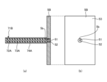
図8は、変形例2に係るグランド板および同軸ケーブルの構成を説明するための図である。図8の(a)は、第2グランド板と同軸ケーブルとが接続した構成の断面図を示す。図8の(b)は、第2グランド板を、同軸ケーブルが接続する側と反対側からみた平面図を示す。本変形例1にかかる測定ユニットは、上述した第2グランド板5に代えて第2グランド板5B、同軸ケーブル71に代えて同軸ケーブル71Bが設けられる。以下、上述した実施の形態と同様の構成については説明を省略する。
第2グランド板5Bには、板厚方向に貫通する貫通孔5bが形成される。貫通孔5bは、第2誘電体52の外周の径と略同等の径で延びる孔である。第2シグナル導体51および第2誘電体52は、第2誘電体52が貫通孔5bに固定される。この際、第2シグナル導体51および第2誘電体52の端面は、第2グランド板5Bの本体部の表面と同一平面上に位置する。
なお、第2シグナル導体51と第1シグナル導体72Aとは、同一の径であることが好ましい。また、第2誘電体52と第1誘電体73Aとは、同一の径であることが好ましい。さらに、第1誘電体73Aおよび第2誘電体52は、同じ材料を用いて構成してもよいし、互いに異なる材料を用いて構成してもよい。
図9は、変形例3に係る同軸ケーブルの構成を説明するための図である。図9の(a)は、同軸ケーブルの断面図を示す。図9の(b)は、同軸ケーブルの平面図を示す。本変形例3にかかる測定ユニットは、上述した第2グランド板5有さず、同軸ケーブル71に代えて同軸ケーブル71Cが設けられる。以下、上述した実施の形態と同様の構成については説明を省略する。
図10は、変形例4に係る同軸ケーブルの構成を説明するための図である。図10の(a)は、同軸ケーブルの断面図を示す。図10の(b)は、同軸ケーブルの平面図を示す。本変形例4にかかる測定ユニットは、上述した第2グランド板5を有さず、同軸ケーブル71に代えて同軸ケーブル71Dが設けられる。以下、上述した実施の形態と同様の構成については説明を省略する。
なお、プローブ2Gは、図11に示す配置や、配設数に限らず、種々の変更が可能である。例えば、二つのプローブ2S間に設けられるプローブ2Gを有しない構成としてもよい。
2 コンタクトプローブ(プローブ)
3 プローブホルダ
4 第1グランド板
5 第2グランド板
6 第1同軸線部
7 第2同軸線部
21 第1プランジャ
22 第2プランジャ
23 コイルばね
31 第1部材
32 第2部材
51 第2シグナル導体
52 第2誘電体
61、71、71A~71D 同軸ケーブル
62、72 シグナル導体
63、73 誘電体
64、74、74A~74C グランド導体
72A 第1シグナル導体
73A 第1誘電体
Claims (8)
- アース用の電位を導通する線路の一部を形成し、一端側の表面が平面をなす第1のグランド部、測定用の信号を導通する線路の一部を形成し、端部が、前記第1のグランド部の前記平面と同一平面上に表出する第1のシグナル部、ならびに、前記第1のグランド部と前記第1のシグナル部との間に設けられ、端部が、前記第1のグランド部および前記第1のシグナル部の前記平面と同一平面上に表出する絶縁性の第1の誘電部を有する第1の接続部と、
アース用の電位を導通する線路の一部を形成し、一端側の表面が平面をなす第2のグランド部、測定用の信号を導通する線路の一部を形成し、端部が、前記第2のグランド部の前記平面と同一平面上に表出する第2のシグナル部、ならびに、前記第2のグランド部と前記第2のシグナル部との間に設けられ、端部が、前記第2のグランド部および前記第2のシグナル部の前記平面と同一平面上に表出する絶縁性の第2の誘電部を有する第2の接続部と、
長手軸に沿って伸縮自在な導電性の第1のコンタクトプローブであって、一端が、前記第1の接続部の前記平面において前記第1のシグナル部に接触し、他端が、前記第2の接続部の前記平面において前記第2のシグナル部に接触する第1のコンタクトプローブと、
長手軸に沿って伸縮自在な導電性の第2のコンタクトプローブであって、一端が、前記第1の接続部の前記平面において前記第1のグランド部に接触し、他端が、前記第2の接続部の前記平面において前記第2のグランド部に接触する第2のコンタクトプローブと、
を備えることを特徴とする測定ユニット。 - 第1のグランド板と、
前記第1のグランド板に接続する第1の同軸ケーブルと、
第2のグランド板と、
前記第2のグランド板に接続する第2の同軸ケーブルと、
を備え、
前記第1の同軸ケーブルは、
前記第1のシグナル部の前記線路の一部を形成する第1のシグナル導体と、
前記第1のシグナル導体の外周に設けられる第1の誘電体と、
前記第1の誘電体の外周に設けられる第1のグランド導体と、
を有し、
前記第2の同軸ケーブルは、
前記第2のシグナル部の前記線路の一部を形成する第2のシグナル導体と、
前記第2のシグナル導体の外周に設けられる第2の誘電体と、
前記第2の誘電体の外周に設けられる第2のグランド導体と、
を有し、
前記第1のシグナル導体が前記第1のシグナル部を構成し、
前記第1の誘電体が前記第1の誘電部を構成し、
前記第1のグランド導体および前記第1のグランド板が前記第1のグランド部を構成し、
前記第2のシグナル導体が前記第2のシグナル部を構成し、
前記第2の誘電体が前記第2の誘電部を構成し、
前記第2のグランド導体および前記第2のグランド板が前記第2のグランド部を構成する、
ことを特徴とする請求項1に記載の測定ユニット。 - 前記第1のグランド板には、前記第1のグランド導体が挿通される第1の貫通孔が形成され、
前記第2のグランド板には、前記第2のグランド導体が挿通される第2の貫通孔が形成される、
ことを特徴とする請求項2に記載の測定ユニット。 - 前記第1のグランド板には、前記第1の誘電体が挿通される第1の貫通孔が形成され、
前記第1のグランド導体は、前記第1のグランド板の表面と電気的に接続し、
前記第2のグランド板には、前記第2の誘電体が挿通される第2の貫通孔が形成され、
前記第2のグランド導体は、前記第2のグランド板の表面と電気的に接続する、
ことを特徴とする請求項2に記載の測定ユニット。 - 第1のグランド板と、
前記第1のグランド板に接続する第1の同軸ケーブルと、
第2のグランド板と、
前記第2のグランド板に接続する第2の同軸ケーブルと、
を備え、
前記第1のグランド板は、
前記第1のシグナル部の前記線路の一部を形成する第1のシグナル中継部と、
前記第1のシグナル中継部の外周を覆う第1のグランド板側誘電体と、
を有し、
前記第2のグランド板は、
前記第2のシグナル部の前記線路の一部を形成する第2のシグナル中継部と、
前記第2のシグナル中継部の外周を覆う第2のグランド板側誘電体と、
を有し、
前記第1の同軸ケーブルは、
前記第1のシグナル部の前記線路の一部を形成し、前記第1のシグナル中継部と電気的に接続する第1のシグナル導体と、
前記第1のシグナル導体の外周に設けられる第1のケーブル側誘電体と、
前記第1のケーブル側誘電体の外周に設けられ、前記第1のグランド板の前記第1のシグナル中継部および前記第1のグランド板側誘電体とは異なる位置において電気的に接続する第1のグランド導体と、
を有し、
前記第2の同軸ケーブルは、
前記第2のシグナル部の前記線路の一部を形成し、前記第2のシグナル中継部と電気的に接続する第2のシグナル導体と、
前記第2のシグナル導体の外周に設けられる第2のケーブル側誘電体と、
前記第2のケーブル側誘電体の外周に設けられ、前記第2のグランド板の前記第2のシグナル中継部および前記第2のグランド板側誘電体とは異なる位置において電気的に接続する第2のグランド導体と、
を有し、
前記第1のシグナル中継部および前記第1のシグナル導体が前記第1のシグナル部を構成し、
前記第1のグランド板側誘電体および前記第1のケーブル側誘電体が前記第1の誘電部を構成し、
前記第1のグランド導体および前記第1のグランド板が前記第1のグランド部を構成し、
前記第2のシグナル中継部および前記第2のシグナル導体が前記第2のシグナル部を構成し、
前記第2のグランド板側誘電体および前記第2のケーブル側誘電体が前記第2の誘電部を構成し、
前記第2のグランド導体および前記第2のグランド板が前記第2のグランド部を構成する、
ことを特徴とする請求項1に記載の測定ユニット。 - 前記第1のグランド板には、複数の前記第1の同軸ケーブルが接続され、
前記第2のグランド板には、複数の前記第2の同軸ケーブルが接続される、
ことを特徴とする請求項2~5のいずれか一つに記載の測定ユニット。 - 前記第1のシグナル部の前記線路を形成する第1のシグナル導体と、前記第1のシグナル導体の外周に設けられ、前記第1の誘電部を構成する第1の誘電体と、前記第1の誘電体の外周に設けられ、前記第1のグランド部を構成する第1のグランド導体とを備える第1の同軸ケーブルと、
前記第2のシグナル部の前記線路を形成する第2のシグナル導体と、前記第2のシグナル導体の外周に設けられ、前記第2の誘電部を構成する第2の誘電体と、前記第2の誘電体の外周に設けられ、前記第2のグランド部を構成する第2のグランド導体とを備える第2の同軸ケーブルと、
を備え、
前記第1のグランド導体は、
前記第1のシグナル導体および前記第1の誘電体に沿って延びる第1の筒状部と、
前記第1の筒状部の一端部に設けられ、平板状をなす第1の平板部と、
を有し、
前記第1のシグナル導体および前記第1の誘電体の端面は、前記第1の平板部の表面と同一平面上に位置し、
前記第2のグランド導体は、
前記第2のシグナル導体および前記第2の誘電体に沿って延びる第2の筒状部と、
前記第2の筒状部の一端部に設けられ、平板状をなす第2の平板部と、
を有し、
前記第2のシグナル導体および前記第2の誘電体の端面は、前記第2の平板部の表面と同一平面上に位置する、
ことを特徴とする請求項1に記載の測定ユニット。 - 前記第1のシグナル導体、前記第1の誘電体および前記第1の筒状部を複数組有し、
前記第2のシグナル導体、前記第2の誘電体および前記第2の筒状部を複数組有する、
ことを特徴とする請求項7に記載の測定ユニット。
Priority Applications (6)
| Application Number | Priority Date | Filing Date | Title |
|---|---|---|---|
| JP2020209745A JP7617735B2 (ja) | 2020-12-17 | 2020-12-17 | 測定ユニット |
| US17/547,400 US20220196704A1 (en) | 2020-12-17 | 2021-12-10 | Measurement unit |
| KR1020210177987A KR102777517B1 (ko) | 2020-12-17 | 2021-12-13 | 측정 유닛 |
| TW110146973A TWI785933B (zh) | 2020-12-17 | 2021-12-15 | 測量單元 |
| CN202111541661.1A CN114646858B (zh) | 2020-12-17 | 2021-12-16 | 测量单元 |
| US18/666,102 US20240302409A1 (en) | 2020-12-17 | 2024-05-16 | Measurement unit |
Applications Claiming Priority (1)
| Application Number | Priority Date | Filing Date | Title |
|---|---|---|---|
| JP2020209745A JP7617735B2 (ja) | 2020-12-17 | 2020-12-17 | 測定ユニット |
Publications (2)
| Publication Number | Publication Date |
|---|---|
| JP2022096563A JP2022096563A (ja) | 2022-06-29 |
| JP7617735B2 true JP7617735B2 (ja) | 2025-01-20 |
Family
ID=81992612
Family Applications (1)
| Application Number | Title | Priority Date | Filing Date |
|---|---|---|---|
| JP2020209745A Active JP7617735B2 (ja) | 2020-12-17 | 2020-12-17 | 測定ユニット |
Country Status (5)
| Country | Link |
|---|---|
| US (2) | US20220196704A1 (ja) |
| JP (1) | JP7617735B2 (ja) |
| KR (1) | KR102777517B1 (ja) |
| CN (1) | CN114646858B (ja) |
| TW (1) | TWI785933B (ja) |
Citations (3)
| Publication number | Priority date | Publication date | Assignee | Title |
|---|---|---|---|---|
| JP2005311525A (ja) | 2004-04-19 | 2005-11-04 | Toyota Central Res & Dev Lab Inc | 伝送線路アンテナ |
| JP2010032531A (ja) | 2000-09-28 | 2010-02-12 | Teradyne Inc | 高性能テスターインタフェースモジュール |
| JP2013224912A (ja) | 2012-04-23 | 2013-10-31 | Furukawa Electric Co Ltd:The | 接続装置および高周波モジュール |
Family Cites Families (22)
| Publication number | Priority date | Publication date | Assignee | Title |
|---|---|---|---|---|
| JPS60123666U (ja) * | 1984-01-30 | 1985-08-20 | 株式会社ヨコオ | 回路基板等の検査装置 |
| JPH01145575A (ja) * | 1987-12-01 | 1989-06-07 | Nec Kyushu Ltd | 同軸形プローブコンタクト |
| JPH0560789A (ja) * | 1991-08-30 | 1993-03-12 | Fujitsu Autom Ltd | 同軸プローブ |
| US6039580A (en) * | 1998-07-16 | 2000-03-21 | Raytheon Company | RF connector having a compliant contact |
| JP2001244308A (ja) * | 2000-02-25 | 2001-09-07 | Mitsubishi Electric Corp | 高周波信号用のプローブ |
| US6686732B2 (en) * | 2001-12-20 | 2004-02-03 | Teradyne, Inc. | Low-cost tester interface module |
| US6951482B1 (en) * | 2004-03-16 | 2005-10-04 | Credence Systems Corporation | Controlled-impedance coaxial cable interconnect system |
| US7053643B2 (en) * | 2004-03-25 | 2006-05-30 | Intel Corporation | Radio frequency (RF) test probe |
| TWM358968U (en) * | 2008-12-31 | 2009-06-11 | Universal Scient Ind Co Ltd | Probe device |
| WO2010117058A1 (ja) * | 2009-04-09 | 2010-10-14 | 日本発條株式会社 | コンタクトプローブおよびプローブユニット |
| JP5353634B2 (ja) * | 2009-10-27 | 2013-11-27 | 住友電気工業株式会社 | 同軸ケーブルハーネス |
| CN106159502B (zh) * | 2011-10-24 | 2018-11-30 | 安达概念股份有限公司 | 使用兼容的互连元件的控制阻抗电缆终端 |
| USRE47459E1 (en) * | 2011-10-24 | 2019-06-25 | Ardent Concepts, Inc. | Controlled-impedance cable termination using compliant interconnect elements |
| CN103917880B (zh) * | 2011-11-09 | 2016-06-08 | 爱德万测试公司 | 用于提取在被测器件与自动测试设备之间进行交换的信号的概念 |
| GB2508568B (en) * | 2012-07-30 | 2017-08-30 | Murata Manufacturing Co | Flat cable |
| CN103884882B (zh) * | 2012-12-21 | 2018-09-25 | 北京普源精电科技有限公司 | 一种多功能的多通道信号获取探头 |
| JP6196191B2 (ja) * | 2014-07-22 | 2017-09-13 | 日本電信電話株式会社 | 測定装置 |
| US9645172B2 (en) * | 2014-10-10 | 2017-05-09 | Samtec, Inc. | Cable assembly |
| TWI569017B (zh) * | 2014-11-14 | 2017-02-01 | Nippon Mektron Kk | Coaxial probe holding mechanism and electrical characteristics check device |
| TWI537566B (zh) * | 2014-11-18 | 2016-06-11 | Mpi Corp | Probe module |
| US10931040B1 (en) * | 2018-08-02 | 2021-02-23 | Ardent Concepts, Inc. | Controlled-impedance circuit board connector assembly |
| WO2020111076A1 (ja) * | 2018-11-27 | 2020-06-04 | 日本発條株式会社 | プローブユニット |
-
2020
- 2020-12-17 JP JP2020209745A patent/JP7617735B2/ja active Active
-
2021
- 2021-12-10 US US17/547,400 patent/US20220196704A1/en not_active Abandoned
- 2021-12-13 KR KR1020210177987A patent/KR102777517B1/ko active Active
- 2021-12-15 TW TW110146973A patent/TWI785933B/zh active
- 2021-12-16 CN CN202111541661.1A patent/CN114646858B/zh active Active
-
2024
- 2024-05-16 US US18/666,102 patent/US20240302409A1/en active Pending
Patent Citations (3)
| Publication number | Priority date | Publication date | Assignee | Title |
|---|---|---|---|---|
| JP2010032531A (ja) | 2000-09-28 | 2010-02-12 | Teradyne Inc | 高性能テスターインタフェースモジュール |
| JP2005311525A (ja) | 2004-04-19 | 2005-11-04 | Toyota Central Res & Dev Lab Inc | 伝送線路アンテナ |
| JP2013224912A (ja) | 2012-04-23 | 2013-10-31 | Furukawa Electric Co Ltd:The | 接続装置および高周波モジュール |
Also Published As
| Publication number | Publication date |
|---|---|
| TW202225698A (zh) | 2022-07-01 |
| US20220196704A1 (en) | 2022-06-23 |
| US20240302409A1 (en) | 2024-09-12 |
| CN114646858B (zh) | 2025-08-12 |
| TWI785933B (zh) | 2022-12-01 |
| JP2022096563A (ja) | 2022-06-29 |
| CN114646858A (zh) | 2022-06-21 |
| KR20220087381A (ko) | 2022-06-24 |
| KR102777517B1 (ko) | 2025-03-06 |
Similar Documents
| Publication | Publication Date | Title |
|---|---|---|
| US7688092B2 (en) | Measuring board for electronic device test apparatus | |
| KR100855208B1 (ko) | 고성능 테스터 인터페이스 모듈 | |
| TWI422829B (zh) | 檢查治具、電極構造及電極構造之製造方法 | |
| US20100244872A1 (en) | Inspection socket and method of producing the same | |
| JP6663084B2 (ja) | プローブユニット | |
| US7332923B2 (en) | Test probe for high-frequency measurement | |
| JP7327659B2 (ja) | 検査用コネクタ及び検査用ユニット | |
| TWI741531B (zh) | 測試裝置 | |
| JP2019138768A (ja) | プローブ | |
| EP3669196B1 (en) | Test device | |
| US20220018877A1 (en) | Probe unit | |
| WO2020137863A1 (ja) | 電気的接続装置 | |
| US9234915B2 (en) | Signal sensing device and circuit boards | |
| KR20220136403A (ko) | 프로브 유닛 | |
| TWI447397B (zh) | 探針卡 | |
| JP3226821U (ja) | 多極コネクタを測定するためのプローブ | |
| TWI785933B (zh) | 測量單元 | |
| KR100950019B1 (ko) | 전기 검사 장치, 이의 제조 방법 및 이의 전기 신호인터페이싱 어셈블리 | |
| JP4979190B2 (ja) | 検査プローブ治具 | |
| KR100921223B1 (ko) | 전선 연결 장치 | |
| KR20090067571A (ko) | 임피던스 측정을 위한 커넥터 | |
| JPH11337576A (ja) | プローブ構造 | |
| JPS62108478A (ja) | 多極同軸コネクタ | |
| TWM449957U (zh) | 探針卡針層結構及使用該結構之探針卡 |
Legal Events
| Date | Code | Title | Description |
|---|---|---|---|
| A621 | Written request for application examination |
Free format text: JAPANESE INTERMEDIATE CODE: A621 Effective date: 20230601 |
|
| A977 | Report on retrieval |
Free format text: JAPANESE INTERMEDIATE CODE: A971007 Effective date: 20240117 |
|
| A131 | Notification of reasons for refusal |
Free format text: JAPANESE INTERMEDIATE CODE: A131 Effective date: 20240123 |
|
| A521 | Request for written amendment filed |
Free format text: JAPANESE INTERMEDIATE CODE: A523 Effective date: 20240322 |
|
| A02 | Decision of refusal |
Free format text: JAPANESE INTERMEDIATE CODE: A02 Effective date: 20240618 |
|
| A521 | Request for written amendment filed |
Free format text: JAPANESE INTERMEDIATE CODE: A523 Effective date: 20240917 |
|
| A911 | Transfer to examiner for re-examination before appeal (zenchi) |
Free format text: JAPANESE INTERMEDIATE CODE: A911 Effective date: 20240925 |
|
| TRDD | Decision of grant or rejection written | ||
| A01 | Written decision to grant a patent or to grant a registration (utility model) |
Free format text: JAPANESE INTERMEDIATE CODE: A01 Effective date: 20241224 |
|
| A61 | First payment of annual fees (during grant procedure) |
Free format text: JAPANESE INTERMEDIATE CODE: A61 Effective date: 20250107 |
|
| R150 | Certificate of patent or registration of utility model |
Ref document number: 7617735 Country of ref document: JP Free format text: JAPANESE INTERMEDIATE CODE: R150 |