JP7620032B2 - 表示パネル、タイリング表示モジュール及びタイリング表示モジュールの製造方法 - Google Patents
表示パネル、タイリング表示モジュール及びタイリング表示モジュールの製造方法 Download PDFInfo
- Publication number
- JP7620032B2 JP7620032B2 JP2022572459A JP2022572459A JP7620032B2 JP 7620032 B2 JP7620032 B2 JP 7620032B2 JP 2022572459 A JP2022572459 A JP 2022572459A JP 2022572459 A JP2022572459 A JP 2022572459A JP 7620032 B2 JP7620032 B2 JP 7620032B2
- Authority
- JP
- Japan
- Prior art keywords
- driving assembly
- light
- thin film
- film transistor
- assembly
- Prior art date
- Legal status (The legal status is an assumption and is not a legal conclusion. Google has not performed a legal analysis and makes no representation as to the accuracy of the status listed.)
- Active
Links
Images




Classifications
-
- G—PHYSICS
- G09—EDUCATION; CRYPTOGRAPHY; DISPLAY; ADVERTISING; SEALS
- G09F—DISPLAYING; ADVERTISING; SIGNS; LABELS OR NAME-PLATES; SEALS
- G09F9/00—Indicating arrangements for variable information in which the information is built-up on a support by selection or combination of individual elements
- G09F9/30—Indicating arrangements for variable information in which the information is built-up on a support by selection or combination of individual elements in which the desired character or characters are formed by combining individual elements
- G09F9/302—Indicating arrangements for variable information in which the information is built-up on a support by selection or combination of individual elements in which the desired character or characters are formed by combining individual elements characterised by the form or geometrical disposition of the individual elements
- G09F9/3026—Video wall, i.e. stackable semiconductor matrix display modules
-
- G—PHYSICS
- G09—EDUCATION; CRYPTOGRAPHY; DISPLAY; ADVERTISING; SEALS
- G09G—ARRANGEMENTS OR CIRCUITS FOR CONTROL OF INDICATING DEVICES USING STATIC MEANS TO PRESENT VARIABLE INFORMATION
- G09G3/00—Control arrangements or circuits, of interest only in connection with visual indicators other than cathode-ray tubes
- G09G3/20—Control arrangements or circuits, of interest only in connection with visual indicators other than cathode-ray tubes for presentation of an assembly of a number of characters, e.g. a page, by composing the assembly by combination of individual elements arranged in a matrix no fixed position being assigned to or needed to be assigned to the individual characters or partial characters
- G09G3/22—Control arrangements or circuits, of interest only in connection with visual indicators other than cathode-ray tubes for presentation of an assembly of a number of characters, e.g. a page, by composing the assembly by combination of individual elements arranged in a matrix no fixed position being assigned to or needed to be assigned to the individual characters or partial characters using controlled light sources
- G09G3/30—Control arrangements or circuits, of interest only in connection with visual indicators other than cathode-ray tubes for presentation of an assembly of a number of characters, e.g. a page, by composing the assembly by combination of individual elements arranged in a matrix no fixed position being assigned to or needed to be assigned to the individual characters or partial characters using controlled light sources using electroluminescent panels
- G09G3/32—Control arrangements or circuits, of interest only in connection with visual indicators other than cathode-ray tubes for presentation of an assembly of a number of characters, e.g. a page, by composing the assembly by combination of individual elements arranged in a matrix no fixed position being assigned to or needed to be assigned to the individual characters or partial characters using controlled light sources using electroluminescent panels semiconductive, e.g. using light-emitting diodes [LED]
-
- H—ELECTRICITY
- H10—SEMICONDUCTOR DEVICES; ELECTRIC SOLID-STATE DEVICES NOT OTHERWISE PROVIDED FOR
- H10H—INORGANIC LIGHT-EMITTING SEMICONDUCTOR DEVICES HAVING POTENTIAL BARRIERS
- H10H29/00—Integrated devices, or assemblies of multiple devices, comprising at least one light-emitting semiconductor element covered by group H10H20/00
- H10H29/30—Active-matrix LED displays
- H10H29/34—Active-matrix LED displays characterised by the geometry or arrangement of subpixels within a pixel, e.g. relative disposition of the RGB subpixels
-
- G—PHYSICS
- G09—EDUCATION; CRYPTOGRAPHY; DISPLAY; ADVERTISING; SEALS
- G09F—DISPLAYING; ADVERTISING; SIGNS; LABELS OR NAME-PLATES; SEALS
- G09F9/00—Indicating arrangements for variable information in which the information is built-up on a support by selection or combination of individual elements
- G09F9/30—Indicating arrangements for variable information in which the information is built-up on a support by selection or combination of individual elements in which the desired character or characters are formed by combining individual elements
- G09F9/33—Indicating arrangements for variable information in which the information is built-up on a support by selection or combination of individual elements in which the desired character or characters are formed by combining individual elements being semiconductor devices, e.g. diodes
-
- G—PHYSICS
- G09—EDUCATION; CRYPTOGRAPHY; DISPLAY; ADVERTISING; SEALS
- G09F—DISPLAYING; ADVERTISING; SIGNS; LABELS OR NAME-PLATES; SEALS
- G09F9/00—Indicating arrangements for variable information in which the information is built-up on a support by selection or combination of individual elements
- G09F9/30—Indicating arrangements for variable information in which the information is built-up on a support by selection or combination of individual elements in which the desired character or characters are formed by combining individual elements
- G09F9/33—Indicating arrangements for variable information in which the information is built-up on a support by selection or combination of individual elements in which the desired character or characters are formed by combining individual elements being semiconductor devices, e.g. diodes
- G09F9/335—Indicating arrangements for variable information in which the information is built-up on a support by selection or combination of individual elements in which the desired character or characters are formed by combining individual elements being semiconductor devices, e.g. diodes being organic light emitting diodes [OLED]
-
- G—PHYSICS
- G09—EDUCATION; CRYPTOGRAPHY; DISPLAY; ADVERTISING; SEALS
- G09G—ARRANGEMENTS OR CIRCUITS FOR CONTROL OF INDICATING DEVICES USING STATIC MEANS TO PRESENT VARIABLE INFORMATION
- G09G3/00—Control arrangements or circuits, of interest only in connection with visual indicators other than cathode-ray tubes
- G09G3/20—Control arrangements or circuits, of interest only in connection with visual indicators other than cathode-ray tubes for presentation of an assembly of a number of characters, e.g. a page, by composing the assembly by combination of individual elements arranged in a matrix no fixed position being assigned to or needed to be assigned to the individual characters or partial characters
- G09G3/22—Control arrangements or circuits, of interest only in connection with visual indicators other than cathode-ray tubes for presentation of an assembly of a number of characters, e.g. a page, by composing the assembly by combination of individual elements arranged in a matrix no fixed position being assigned to or needed to be assigned to the individual characters or partial characters using controlled light sources
- G09G3/30—Control arrangements or circuits, of interest only in connection with visual indicators other than cathode-ray tubes for presentation of an assembly of a number of characters, e.g. a page, by composing the assembly by combination of individual elements arranged in a matrix no fixed position being assigned to or needed to be assigned to the individual characters or partial characters using controlled light sources using electroluminescent panels
- G09G3/32—Control arrangements or circuits, of interest only in connection with visual indicators other than cathode-ray tubes for presentation of an assembly of a number of characters, e.g. a page, by composing the assembly by combination of individual elements arranged in a matrix no fixed position being assigned to or needed to be assigned to the individual characters or partial characters using controlled light sources using electroluminescent panels semiconductive, e.g. using light-emitting diodes [LED]
- G09G3/3208—Control arrangements or circuits, of interest only in connection with visual indicators other than cathode-ray tubes for presentation of an assembly of a number of characters, e.g. a page, by composing the assembly by combination of individual elements arranged in a matrix no fixed position being assigned to or needed to be assigned to the individual characters or partial characters using controlled light sources using electroluminescent panels semiconductive, e.g. using light-emitting diodes [LED] organic, e.g. using organic light-emitting diodes [OLED]
- G09G3/3225—Control arrangements or circuits, of interest only in connection with visual indicators other than cathode-ray tubes for presentation of an assembly of a number of characters, e.g. a page, by composing the assembly by combination of individual elements arranged in a matrix no fixed position being assigned to or needed to be assigned to the individual characters or partial characters using controlled light sources using electroluminescent panels semiconductive, e.g. using light-emitting diodes [LED] organic, e.g. using organic light-emitting diodes [OLED] using an active matrix
-
- G—PHYSICS
- G09—EDUCATION; CRYPTOGRAPHY; DISPLAY; ADVERTISING; SEALS
- G09G—ARRANGEMENTS OR CIRCUITS FOR CONTROL OF INDICATING DEVICES USING STATIC MEANS TO PRESENT VARIABLE INFORMATION
- G09G3/00—Control arrangements or circuits, of interest only in connection with visual indicators other than cathode-ray tubes
- G09G3/20—Control arrangements or circuits, of interest only in connection with visual indicators other than cathode-ray tubes for presentation of an assembly of a number of characters, e.g. a page, by composing the assembly by combination of individual elements arranged in a matrix no fixed position being assigned to or needed to be assigned to the individual characters or partial characters
- G09G3/22—Control arrangements or circuits, of interest only in connection with visual indicators other than cathode-ray tubes for presentation of an assembly of a number of characters, e.g. a page, by composing the assembly by combination of individual elements arranged in a matrix no fixed position being assigned to or needed to be assigned to the individual characters or partial characters using controlled light sources
- G09G3/30—Control arrangements or circuits, of interest only in connection with visual indicators other than cathode-ray tubes for presentation of an assembly of a number of characters, e.g. a page, by composing the assembly by combination of individual elements arranged in a matrix no fixed position being assigned to or needed to be assigned to the individual characters or partial characters using controlled light sources using electroluminescent panels
- G09G3/32—Control arrangements or circuits, of interest only in connection with visual indicators other than cathode-ray tubes for presentation of an assembly of a number of characters, e.g. a page, by composing the assembly by combination of individual elements arranged in a matrix no fixed position being assigned to or needed to be assigned to the individual characters or partial characters using controlled light sources using electroluminescent panels semiconductive, e.g. using light-emitting diodes [LED]
- G09G3/3208—Control arrangements or circuits, of interest only in connection with visual indicators other than cathode-ray tubes for presentation of an assembly of a number of characters, e.g. a page, by composing the assembly by combination of individual elements arranged in a matrix no fixed position being assigned to or needed to be assigned to the individual characters or partial characters using controlled light sources using electroluminescent panels semiconductive, e.g. using light-emitting diodes [LED] organic, e.g. using organic light-emitting diodes [OLED]
- G09G3/3225—Control arrangements or circuits, of interest only in connection with visual indicators other than cathode-ray tubes for presentation of an assembly of a number of characters, e.g. a page, by composing the assembly by combination of individual elements arranged in a matrix no fixed position being assigned to or needed to be assigned to the individual characters or partial characters using controlled light sources using electroluminescent panels semiconductive, e.g. using light-emitting diodes [LED] organic, e.g. using organic light-emitting diodes [OLED] using an active matrix
- G09G3/3233—Control arrangements or circuits, of interest only in connection with visual indicators other than cathode-ray tubes for presentation of an assembly of a number of characters, e.g. a page, by composing the assembly by combination of individual elements arranged in a matrix no fixed position being assigned to or needed to be assigned to the individual characters or partial characters using controlled light sources using electroluminescent panels semiconductive, e.g. using light-emitting diodes [LED] organic, e.g. using organic light-emitting diodes [OLED] using an active matrix with pixel circuitry controlling the current through the light-emitting element
-
- H—ELECTRICITY
- H10—SEMICONDUCTOR DEVICES; ELECTRIC SOLID-STATE DEVICES NOT OTHERWISE PROVIDED FOR
- H10H—INORGANIC LIGHT-EMITTING SEMICONDUCTOR DEVICES HAVING POTENTIAL BARRIERS
- H10H29/00—Integrated devices, or assemblies of multiple devices, comprising at least one light-emitting semiconductor element covered by group H10H20/00
- H10H29/01—Manufacture or treatment
- H10H29/012—Manufacture or treatment of active-matrix LED displays
-
- H—ELECTRICITY
- H10—SEMICONDUCTOR DEVICES; ELECTRIC SOLID-STATE DEVICES NOT OTHERWISE PROVIDED FOR
- H10H—INORGANIC LIGHT-EMITTING SEMICONDUCTOR DEVICES HAVING POTENTIAL BARRIERS
- H10H29/00—Integrated devices, or assemblies of multiple devices, comprising at least one light-emitting semiconductor element covered by group H10H20/00
- H10H29/20—Assemblies of multiple devices comprising at least one light-emitting semiconductor device covered by group H10H20/00
- H10H29/24—Assemblies of multiple devices comprising at least one light-emitting semiconductor device covered by group H10H20/00 comprising multiple light-emitting semiconductor devices
-
- H—ELECTRICITY
- H10—SEMICONDUCTOR DEVICES; ELECTRIC SOLID-STATE DEVICES NOT OTHERWISE PROVIDED FOR
- H10H—INORGANIC LIGHT-EMITTING SEMICONDUCTOR DEVICES HAVING POTENTIAL BARRIERS
- H10H29/00—Integrated devices, or assemblies of multiple devices, comprising at least one light-emitting semiconductor element covered by group H10H20/00
- H10H29/30—Active-matrix LED displays
- H10H29/49—Interconnections, e.g. wiring lines or terminals
-
- G—PHYSICS
- G09—EDUCATION; CRYPTOGRAPHY; DISPLAY; ADVERTISING; SEALS
- G09G—ARRANGEMENTS OR CIRCUITS FOR CONTROL OF INDICATING DEVICES USING STATIC MEANS TO PRESENT VARIABLE INFORMATION
- G09G2300/00—Aspects of the constitution of display devices
- G09G2300/02—Composition of display devices
- G09G2300/026—Video wall, i.e. juxtaposition of a plurality of screens to create a display screen of bigger dimensions
-
- G—PHYSICS
- G09—EDUCATION; CRYPTOGRAPHY; DISPLAY; ADVERTISING; SEALS
- G09G—ARRANGEMENTS OR CIRCUITS FOR CONTROL OF INDICATING DEVICES USING STATIC MEANS TO PRESENT VARIABLE INFORMATION
- G09G2300/00—Aspects of the constitution of display devices
- G09G2300/04—Structural and physical details of display devices
- G09G2300/0421—Structural details of the set of electrodes
- G09G2300/0426—Layout of electrodes and connections
Landscapes
- Engineering & Computer Science (AREA)
- Physics & Mathematics (AREA)
- General Physics & Mathematics (AREA)
- Theoretical Computer Science (AREA)
- Computer Hardware Design (AREA)
- Devices For Indicating Variable Information By Combining Individual Elements (AREA)
- Microelectronics & Electronic Packaging (AREA)
- Optics & Photonics (AREA)
- Multimedia (AREA)
- Electroluminescent Light Sources (AREA)
- Transforming Electric Information Into Light Information (AREA)
Description
表示パネルであって、前記表示パネルは、第一表示領域と、第二表示領域と、を含み、前記第二表示領域は、少なくとも第一方向に沿って前記第一表示領域の一側の周囲に設けられ、
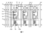
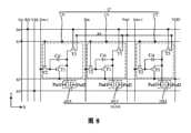
前記表示パネルは、前記第二表示領域に設けられる複数の第一画素組を含み、前記第一画素組は、第一駆動アセンブリと、第二駆動アセンブリと、第一発光アセンブリと、第二発光アセンブリと、を含み、前記第一駆動アセンブリは、前記第一発光アセンブリに電気的に接続され、前記第二駆動アセンブリは、前記第二発光アセンブリに電気的に接続され、前記第一画素組において、前記第一駆動アセンブリは、前記第一方向に沿って第一発光アセンブリの一側に設けられ、前記第二駆動アセンブリは、前記第一方向に沿って前記第一駆動アセンブリの前記第一発光アセンブリから離れた一側に設けられ、前記第二発光アセンブリは、前記第一方向に沿って前記第二駆動アセンブリの前記第一駆動アセンブリから離れた一側に設けられる、
表示パネルを提供する。
前記第一画素組において、前記第一駆動アセンブリと、前記第二駆動アセンブリとは、軸対称に設けられ、且つ前記第一駆動アセンブリと、前記第二駆動アセンブリとの構造は同一である。
前記表示パネルは、複数の第二画素組をさらに含み、前記複数の第二画素組は、前記第一表示領域に設けられ、前記複数の第一画素組及び前記複数の第二画素組は、アレイ状に分布する。
前記第一画素組の構造と、前記第二画素組の構造とは同一である。
前記第一画素組の画素間隔は、前記第二画素組の画素間隔に等しい。
前記第一駆動アセンブリは、少なくとも一つの第一薄膜トランジスタを含み、前記第一発光アセンブリは、少なくとも一つの発光デバイスを含み、前記第一薄膜トランジスタは、対応する前記発光デバイスに電気的に接続される。
前記表示パネルは、複数本のゲート線と、複数本のデータ線と、複数本の第一電源線と、複数本の第二電源線と、をさらに含み、
前記第一駆動アセンブリは、少なくとも一つの第二薄膜トランジスタをさらに含み、前記第二薄膜トランジスタの制御端は、前記ゲート線に電気的に接続され、前記第二薄膜トランジスタの入力端は、前記データ線に電気的に接続され、前記第二薄膜トランジスタの出力端は、前記第一薄膜トランジスタの制御端に電気的に接続され、前記第一薄膜トランジスタの入力端は、前記第一電源線に電気的に接続され、
前記発光デバイスは、第一ピンと、第二ピンと、を有し、前記第一薄膜トランジスタの出力端は、前記発光デバイスの第一ピンに電気的に接続され、前記発光デバイスの第二ピンは、前記第二電源線に電気的に接続される。
前記第一駆動アセンブリは、少なくとも一つの蓄積キャパシタをさらに含み、前記第二薄膜トランジスタの出力端は、前記蓄積キャパシタを介して、前記第一薄膜トランジスタの出力端と接続される。
前記表示パネルは、第一信号線と、第二信号線と、をさらに含み、
前記第一駆動アセンブリは、少なくとも一つの第三薄膜トランジスタをさらに含み、前記第三薄膜トランジスタの制御端と、前記第一信号線とは電気的に接続され、前記第三薄膜トランジスタの入力端と、前記第二信号線とは電気的に接続され、前記第三薄膜トランジスタの出力端と、前記第一薄膜トランジスタの出力端とは電気的に接続される。
少なくとも二つの表示パネルを含み、前記少なくとも二つの表示パネルは、タイリングされ、前記表示パネルは、上述した表示パネルが採用される、
タイリング表示モジュールをさらに提供する。
前記第一画素組において、前記第一駆動アセンブリと、前記第二駆動アセンブリとは、軸対称に設けられ、且つ前記第一駆動アセンブリと、前記第二駆動アセンブリとの構造は同一である。
前記表示パネルは、複数の第二画素組をさらに含み、前記複数の第二画素組は、前記第一表示領域に設けられ、前記複数の第一画素組及び前記複数の第二画素組は、アレイ状に分布する。
前記第一画素組の構造と、前記第二画素組の構造とは同一である。
前記第一画素組の画素間隔は、前記第二画素組の画素間隔に等しい。
前記第一駆動アセンブリは、少なくとも一つの第一薄膜トランジスタを含み、前記第一発光アセンブリは、少なくとも一つの発光デバイスを含み、前記第一薄膜トランジスタは、対応する前記発光デバイスに電気的に接続される。
前記表示パネルは、複数本のゲート線と、複数本のデータ線と、複数本の第一電源線と、複数本の第二電源線と、をさらに含み、
前記第一駆動アセンブリは、少なくとも一つの第二薄膜トランジスタをさらに含み、前記第二薄膜トランジスタの制御端は、前記ゲート線に電気的に接続され、前記第二薄膜トランジスタの入力端は、前記データ線に電気的に接続され、前記第二薄膜トランジスタの出力端は、前記第一薄膜トランジスタの制御端に電気的に接続され、前記第一薄膜トランジスタの入力端は、前記第一電源線に電気的に接続され、
前記発光デバイスは、第一ピンと、第二ピンと、を有し、前記第一薄膜トランジスタの出力端は、前記発光デバイスの第一ピンに電気的に接続され、前記発光デバイスの第二ピンは、前記第二電源線に電気的に接続される。
前記第一駆動アセンブリは、少なくとも一つの蓄積キャパシタをさらに含み、前記第二薄膜トランジスタの出力端は、前記蓄積キャパシタを介して、前記第一薄膜トランジスタの出力端と接続される。
前記表示パネルは、第一信号線と、第二信号線と、をさらに含み、
前記第一駆動アセンブリは、少なくとも一つの第三薄膜トランジスタをさらに含み、前記第三薄膜トランジスタの制御端と、前記第一信号線とは電気的に接続され、前記第三薄膜トランジスタの入力端と、前記第二信号線とは電気的に接続され、前記第三薄膜トランジスタの出力端と、前記第一薄膜トランジスタの出力端とは電気的に接続される。
少なくとも二つの表示パネルを提供し、前記表示パネルは、第一表示領域と、第二表示領域と、負の公差領域と、を含み、前記第二表示領域は、少なくとも第一方向に沿って前記第一表示領域の周囲に設けられ、前記負の公差領域は、前記第二表示領域の前記第一表示領域から離れた一側に設けられ、前記第二表示領域は、複数の第一画素組が設けられ、前記第一画素組は、第一駆動アセンブリと、第二駆動アセンブリと、第一発光アセンブリと、第二発光アセンブリと、を含み、前記第一駆動アセンブリは、前記第一発光アセンブリに電気的に接続され、前記第二駆動アセンブリは、前記第二発光アセンブリに電気的に接続され、前記第一画素組において、前記第一駆動アセンブリは、前記第一方向に沿って第一発光アセンブリの一側に設けられ、前記第二駆動アセンブリは、前記第一方向に沿って前記第一駆動アセンブリの前記第一発光アセンブリから離れた一側に設けられ、前記第二発光アセンブリは、前記第一方向に沿って前記第二駆動アセンブリの前記第一駆動アセンブリから離れた一側に設けられる、ステップB1と、
前記表示パネルの負の公差領域を除去する、ステップB2と、
少なくとも二つの前記表示パネルを互いにタイリングして、タイリング表示モジュールを得る、ステップB3と、を含む、
タイリング表示モジュールの製造方法をさらに提供する。
前記ステップB1において、前記負の公差領域の幅は、0.2ミリメートル以上であり、且つ前記負の公差領域の幅は、0.6ミリメートル以下である。
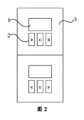
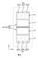
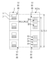
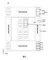
図6に示すように、少なくとも二つの表示パネル10を提供し、表示パネル10は、上述した実施例の表示パネル10が採用され、且つ表示パネル10は、負の公差領域NTAをさらに含み、負の公差領域NTAは、第二表示領域AA2の第一表示領域AA1から離れた一側に設けられる、ステップB1と、
図6に示すように、表示パネル10の負の公差領域NTAを除去し、具体的には、レーザ切断及び研磨等の方式によって表示パネル10の負の公差領域NTAを除去することができるが、これに限定しない、ステップB2と、
図13に示すように、少なくとも二つの表示パネル10を互いにタイリングして、タイリング表示モジュールを得る、ステップB3と、を含む、
タイリング表示モジュールの製造方法をさらに提供する。
2:発光アセンブリ
3:負の公差領域
10:表示パネル
11:基板
12:バッファ層
13:ゲート絶縁層
14:層間絶縁層
15:パッシベーション層
16:第一発光アセンブリ
17:第一駆動アセンブリ
18:第二駆動アセンブリ
19:第二発光アセンブリ
161:発光デバイス
171:副駆動組
1611:赤色発光デバイス
1612:緑色発光デバイス
1613:青色発光デバイス
1614:第一ピン
1615:第二ピン
AA1:第一表示領域
AA2:第二表示領域
AL1:第一活性層
AL2:第二活性層
AL3:第三活性層
Cst:蓄積キャパシタ
C1:第一キャパシタ
C2:第二キャパシタ
D:データ線
DE1:第一ドレイン
DE2:第二ドレイン
DE3:第三ドレイン
G:ゲート線
GE1:第一ゲート
GE2:第二ゲート
GE3:第三ゲート
LS1:第一遮光電極
LS2:第二遮光電極
LS3:第三遮光電極
NTA:負の公差領域
Pad1:第一パッド
Pad2:第二パッド
PG1:第一画素組
PG2:第二画素組
P1:第一画素ユニット
P2:第二画素ユニット
RD:第一信号線
SE1:第一ソース
SE2:第二ソース
SE3:第三ソース
S1:第一切り替え線
S2:第二切り替え線
S3:第三切り替え線
S4:第四切り替え線
S5:第五切り替え線
T1:第一薄膜トランジスタ
T2:第二薄膜トランジスタ
T3:第三薄膜トランジスタ
VDD:第一電源線
Vref:第二信号線
VSS:第二電源線
X:第二方向
Y:第一方向
Claims (12)
- 表示パネルであって、前記表示パネルは、第一表示領域と、第二表示領域と、を含み、前記第二表示領域は、少なくとも第一方向に沿って前記第一表示領域の周囲に設けられ、
前記表示パネルは、前記第二表示領域に設けられる複数の第一画素組と、前記第一方向に沿って延伸される複数のゲート線と、複数のデータ線と、複数の第一電源線と、複数の第二電源線とを含み、
前記第一画素組は、第一画素ユニットと、第二画素ユニットとを含み、前記第一画素ユニットは、第一駆動アセンブリと第一発光アセンブリとを含み、前記第二画素ユニットは、第二駆動アセンブリと第二発光アセンブリとを含み、
前記第一駆動アセンブリは、前記第一発光アセンブリに電気的に接続され、前記第二駆動アセンブリは、前記第二発光アセンブリに電気的に接続され、前記第一画素組において、前記第一駆動アセンブリは、前記第一方向に沿って前記第一発光アセンブリの一側に設けられ、前記第二駆動アセンブリは、前記第一方向に沿って前記第一駆動アセンブリの前記第一発光アセンブリから離れた一側に設けられ、前記第二発光アセンブリは、前記第一方向に沿って前記第二駆動アセンブリの前記第一駆動アセンブリから離れた一側に設けられ、
前記ゲート線及び前記第一電源線は、第二方向に沿って前記第一画素ユニット及び前記第二画素ユニットの相対する二つの側に設置され、前記第二電源線は、前記ゲート線の前記第一電源線に近い一側に設けられ、前記データ線は、前記第一電源線と、前記第二電源線との間に設置され、前記第一駆動アセンブリ、前記第二駆動アセンブリ、前記第一発光アセンブリ及び前記第二発光アセンブリは、前記第一電源線と、前記第二電源線との間に位置する、
表示パネル。 - 前記第一画素組において、前記第一駆動アセンブリと、前記第二駆動アセンブリとは、軸対称に設けられ、且つ前記第一駆動アセンブリと、前記第二駆動アセンブリとの構造は同一である、
請求項1に記載の表示パネル。 - 複数の第二画素組をさらに含み、前記複数の第二画素組は、前記第一表示領域に設けられ、前記複数の第一画素組及び前記複数の第二画素組は、アレイ状に分布する、
請求項1に記載の表示パネル。 - 前記第一画素組の構造と、前記第二画素組の構造とは同一である、
請求項3に記載の表示パネル。 - 前記第一画素組の画素間隔は、前記第二画素組の画素間隔に等しい、
請求項3に記載の表示パネル。 - 前記第一駆動アセンブリは、少なくとも一つの第一薄膜トランジスタを含み、前記第一発光アセンブリは、少なくとも一つの発光デバイスを含み、前記第一薄膜トランジスタは、対応する前記発光デバイスに電気的に接続される、
請求項1に記載の表示パネル。 - 前記第一駆動アセンブリは、少なくとも一つの第二薄膜トランジスタをさらに含み、前記第二薄膜トランジスタの制御端は、前記ゲート線に電気的に接続され、前記第二薄膜トランジスタの入力端は、前記データ線に電気的に接続され、前記第二薄膜トランジスタの出力端は、前記第一薄膜トランジスタの制御端に電気的に接続され、前記第一薄膜トランジスタの入力端は、前記第一電源線に電気的に接続され、
前記発光デバイスは、第一ピンと、第二ピンと、を有し、前記第一薄膜トランジスタの出力端は、前記発光デバイスの第一ピンに電気的に接続され、前記発光デバイスの第二ピンは、前記第二電源線に電気的に接続される、
請求項6に記載の表示パネル。 - 前記第一駆動アセンブリは、少なくとも一つの蓄積キャパシタをさらに含み、前記第二薄膜トランジスタの出力端は、前記蓄積キャパシタを介して、前記第一薄膜トランジスタの出力端と接続される、
請求項7に記載の表示パネル。 - 第一信号線と、第二信号線と、をさらに含み、
前記第一駆動アセンブリは、少なくとも一つの第三薄膜トランジスタをさらに含み、前記第三薄膜トランジスタの制御端と、前記第一信号線とは電気的に接続され、前記第三薄膜トランジスタの入力端と、前記第二信号線とは電気的に接続され、前記第三薄膜トランジスタの出力端と、前記第一薄膜トランジスタの出力端とは電気的に接続される、
請求項6に記載の表示パネル。 - 少なくとも二つの表示パネルを含み、前記少なくとも二つの表示パネルは、タイリングされ、前記表示パネルは、請求項1~9のいずれか一項に記載の表示パネルが採用される、
タイリング表示モジュール。 - 少なくとも二つの表示パネルを提供し、前記表示パネルは、第一表示領域と、第二表示領域と、負の公差領域と、を含み、前記第二表示領域は、少なくとも第一方向に沿って前記第一表示領域の周囲に設けられ、前記負の公差領域は、前記第二表示領域の前記第一表示領域から離れた一側に設けられ、前記第二表示領域は、複数の第一画素組が設けられ、前記第一画素組は、第一駆動アセンブリと、第二駆動アセンブリと、第一発光アセンブリと、第二発光アセンブリと、を含み、前記第一駆動アセンブリは、前記第一発光アセンブリに電気的に接続され、前記第二駆動アセンブリは、前記第二発光アセンブリに電気的に接続され、前記第一画素組において、前記第一駆動アセンブリは、前記第一方向に沿って前記第一発光アセンブリの一側に設けられ、前記第二駆動アセンブリは、前記第一方向に沿って前記第一駆動アセンブリの前記第一発光アセンブリから離れた一側に設けられ、前記第二発光アセンブリは、前記第一方向に沿って前記第二駆動アセンブリの前記第一駆動アセンブリから離れた一側に設けられる、ステップB1と、
前記表示パネルの前記負の公差領域を除去する、ステップB2と、
少なくとも二つの前記表示パネルを互いにタイリングして、タイリング表示モジュールを得る、ステップB3と、を含む、
請求項10に記載のタイリング表示モジュールの製造方法。 - 前記ステップB1において、前記負の公差領域の幅は、0.2ミリメートル以上であり、且つ前記負の公差領域の幅は、0.6ミリメートル以下である、
請求項11に記載のタイリング表示モジュールの製造方法。
Applications Claiming Priority (3)
| Application Number | Priority Date | Filing Date | Title |
|---|---|---|---|
| CN202210843822.0A CN115273677B (zh) | 2022-07-18 | 2022-07-18 | 显示面板、拼接显示模组以及拼接显示模组的制作方法 |
| CN202210843822.0 | 2022-07-18 | ||
| PCT/CN2022/110757 WO2024016394A1 (zh) | 2022-07-18 | 2022-08-08 | 显示面板、拼接显示模组以及拼接显示模组的制作方法 |
Publications (2)
| Publication Number | Publication Date |
|---|---|
| JP2024531001A JP2024531001A (ja) | 2024-08-29 |
| JP7620032B2 true JP7620032B2 (ja) | 2025-01-22 |
Family
ID=83767646
Family Applications (1)
| Application Number | Title | Priority Date | Filing Date |
|---|---|---|---|
| JP2022572459A Active JP7620032B2 (ja) | 2022-07-18 | 2022-08-08 | 表示パネル、タイリング表示モジュール及びタイリング表示モジュールの製造方法 |
Country Status (5)
| Country | Link |
|---|---|
| US (1) | US20250386635A1 (ja) |
| EP (1) | EP4560611A4 (ja) |
| JP (1) | JP7620032B2 (ja) |
| CN (1) | CN115273677B (ja) |
| WO (1) | WO2024016394A1 (ja) |
Families Citing this family (2)
| Publication number | Priority date | Publication date | Assignee | Title |
|---|---|---|---|---|
| CN115938236B (zh) * | 2022-12-12 | 2024-08-09 | 湖北长江新型显示产业创新中心有限公司 | 显示面板、拼接显示装置及其制备方法 |
| TWI889277B (zh) | 2024-04-08 | 2025-07-01 | 友達光電股份有限公司 | 顯示面板 |
Citations (10)
| Publication number | Priority date | Publication date | Assignee | Title |
|---|---|---|---|---|
| JP2013089475A (ja) | 2011-10-19 | 2013-05-13 | Canon Inc | 発光表示装置及びその製造方法 |
| CN211858095U (zh) | 2020-04-27 | 2020-11-03 | 重庆康佳光电技术研究院有限公司 | 一种显示面板及拼接显示装置 |
| CN112991964A (zh) | 2021-03-29 | 2021-06-18 | 上海天马微电子有限公司 | 显示面板、显示装置及显示面板的制作方法 |
| US20210217353A1 (en) | 2019-11-29 | 2021-07-15 | Boe Technology Group Co., Ltd. | Array substrate, display panel, spliced display panel and display driving method |
| US20210327857A1 (en) | 2020-04-21 | 2021-10-21 | Samsung Display Co., Ltd. | Display device and tiled display device having the same |
| CN214752699U (zh) | 2021-02-25 | 2021-11-16 | 广州视源电子科技股份有限公司 | Led显示模组及显示屏 |
| US20220052030A1 (en) | 2020-03-18 | 2022-02-17 | Beijing Boe Optoelectronics Technology Co., Ltd. | Display Panel and Display Apparatus |
| CN114141156A (zh) | 2021-12-09 | 2022-03-04 | 惠州华星光电显示有限公司 | 一种拼接屏及显示装置 |
| CN114497103A (zh) | 2020-10-26 | 2022-05-13 | 佛山市国星光电股份有限公司 | 一种可拼接的显示模块、制备方法及显示装置 |
| CN114648923A (zh) | 2022-03-16 | 2022-06-21 | Tcl华星光电技术有限公司 | 一种拼接屏及显示装置 |
Family Cites Families (4)
| Publication number | Priority date | Publication date | Assignee | Title |
|---|---|---|---|---|
| CN107658326A (zh) * | 2017-03-20 | 2018-02-02 | 广东聚华印刷显示技术有限公司 | 电致发光显示器件及其像素结构和制作方法 |
| KR102427082B1 (ko) * | 2017-12-15 | 2022-07-29 | 엘지디스플레이 주식회사 | 마이크로led 표시장치 및 그 구동방법 |
| KR102589620B1 (ko) * | 2018-10-29 | 2023-10-17 | 삼성전자주식회사 | 표시 장치 및 이의 제조 방법 |
| CN113223420B (zh) * | 2021-05-06 | 2023-04-21 | 湖北长江新型显示产业创新中心有限公司 | 一种显示面板及显示装置 |
-
2022
- 2022-07-18 CN CN202210843822.0A patent/CN115273677B/zh active Active
- 2022-08-08 EP EP22757820.0A patent/EP4560611A4/en active Pending
- 2022-08-08 US US17/799,662 patent/US20250386635A1/en active Pending
- 2022-08-08 WO PCT/CN2022/110757 patent/WO2024016394A1/zh not_active Ceased
- 2022-08-08 JP JP2022572459A patent/JP7620032B2/ja active Active
Patent Citations (10)
| Publication number | Priority date | Publication date | Assignee | Title |
|---|---|---|---|---|
| JP2013089475A (ja) | 2011-10-19 | 2013-05-13 | Canon Inc | 発光表示装置及びその製造方法 |
| US20210217353A1 (en) | 2019-11-29 | 2021-07-15 | Boe Technology Group Co., Ltd. | Array substrate, display panel, spliced display panel and display driving method |
| US20220052030A1 (en) | 2020-03-18 | 2022-02-17 | Beijing Boe Optoelectronics Technology Co., Ltd. | Display Panel and Display Apparatus |
| US20210327857A1 (en) | 2020-04-21 | 2021-10-21 | Samsung Display Co., Ltd. | Display device and tiled display device having the same |
| CN211858095U (zh) | 2020-04-27 | 2020-11-03 | 重庆康佳光电技术研究院有限公司 | 一种显示面板及拼接显示装置 |
| CN114497103A (zh) | 2020-10-26 | 2022-05-13 | 佛山市国星光电股份有限公司 | 一种可拼接的显示模块、制备方法及显示装置 |
| CN214752699U (zh) | 2021-02-25 | 2021-11-16 | 广州视源电子科技股份有限公司 | Led显示模组及显示屏 |
| CN112991964A (zh) | 2021-03-29 | 2021-06-18 | 上海天马微电子有限公司 | 显示面板、显示装置及显示面板的制作方法 |
| CN114141156A (zh) | 2021-12-09 | 2022-03-04 | 惠州华星光电显示有限公司 | 一种拼接屏及显示装置 |
| CN114648923A (zh) | 2022-03-16 | 2022-06-21 | Tcl华星光电技术有限公司 | 一种拼接屏及显示装置 |
Also Published As
| Publication number | Publication date |
|---|---|
| US20250386635A1 (en) | 2025-12-18 |
| WO2024016394A1 (zh) | 2024-01-25 |
| CN115273677A (zh) | 2022-11-01 |
| EP4560611A1 (en) | 2025-05-28 |
| CN115273677B (zh) | 2024-03-15 |
| EP4560611A4 (en) | 2026-01-07 |
| JP2024531001A (ja) | 2024-08-29 |
Similar Documents
| Publication | Publication Date | Title |
|---|---|---|
| JP7676600B2 (ja) | アレイ基板、表示パネル、スプライシング表示パネル、及び表示駆動方法 | |
| US12111541B2 (en) | Display device | |
| CN114300505B (zh) | 发光模组和显示装置 | |
| US8405646B2 (en) | Display panel and active device array substrate thereof | |
| CN104238212A (zh) | 液晶显示装置及其驱动方法 | |
| JP2022501629A (ja) | フレキシブルマイクロ発光ダイオード表示パネル及びマイクロ発光ダイオード表示装置 | |
| JP7620032B2 (ja) | 表示パネル、タイリング表示モジュール及びタイリング表示モジュールの製造方法 | |
| TW202010120A (zh) | 微型發光二極體顯示裝置 | |
| CN205080891U (zh) | 显示装置及显示面板 | |
| WO2020062369A1 (zh) | 一种阵列基板和显示面板 | |
| TWI432861B (zh) | 液晶顯示面板 | |
| US12455713B2 (en) | Display apparatus | |
| WO2022027760A1 (zh) | 背光模组及显示装置 | |
| WO2024145918A1 (zh) | 显示面板和显示装置 | |
| US20220044642A1 (en) | Backlight module and display device having same | |
| US20210011321A1 (en) | Display device and method for manufacturing the same | |
| CN115989538A (zh) | 显示设备和用于制造该显示设备的方法 | |
| KR20230028376A (ko) | 반도체 발광소자를 포함하는 디스플레이 장치 | |
| CN114695428B (zh) | 显示面板及显示装置 | |
| US12555515B2 (en) | Display apparatus | |
| CN212967706U (zh) | 一种led显示单元及显示装置 | |
| WO2025247173A1 (zh) | 显示面板及显示装置 | |
| TW202417950A (zh) | 發光模組、發光基板和顯示裝置 | |
| KR20240125141A (ko) | 자발광 소자를 포함하는 디스플레이 모듈 | |
| CN118519296A (zh) | 显示模组及显示装置 |
Legal Events
| Date | Code | Title | Description |
|---|---|---|---|
| A621 | Written request for application examination |
Free format text: JAPANESE INTERMEDIATE CODE: A621 Effective date: 20221124 |
|
| A131 | Notification of reasons for refusal |
Free format text: JAPANESE INTERMEDIATE CODE: A131 Effective date: 20240903 |
|
| A521 | Request for written amendment filed |
Free format text: JAPANESE INTERMEDIATE CODE: A523 Effective date: 20241129 |
|
| TRDD | Decision of grant or rejection written | ||
| A01 | Written decision to grant a patent or to grant a registration (utility model) |
Free format text: JAPANESE INTERMEDIATE CODE: A01 Effective date: 20241210 |
|
| A61 | First payment of annual fees (during grant procedure) |
Free format text: JAPANESE INTERMEDIATE CODE: A61 Effective date: 20250109 |
|
| R150 | Certificate of patent or registration of utility model |
Ref document number: 7620032 Country of ref document: JP Free format text: JAPANESE INTERMEDIATE CODE: R150 |