JP7623309B2 - ウエハ載置台 - Google Patents
ウエハ載置台 Download PDFInfo
- Publication number
- JP7623309B2 JP7623309B2 JP2022002885A JP2022002885A JP7623309B2 JP 7623309 B2 JP7623309 B2 JP 7623309B2 JP 2022002885 A JP2022002885 A JP 2022002885A JP 2022002885 A JP2022002885 A JP 2022002885A JP 7623309 B2 JP7623309 B2 JP 7623309B2
- Authority
- JP
- Japan
- Prior art keywords
- electrode
- hole
- terminal
- power supply
- wafer
- Prior art date
- Legal status (The legal status is an assumption and is not a legal conclusion. Google has not performed a legal analysis and makes no representation as to the accuracy of the status listed.)
- Active
Links
Images




Classifications
-
- H—ELECTRICITY
- H01—ELECTRIC ELEMENTS
- H01J—ELECTRIC DISCHARGE TUBES OR DISCHARGE LAMPS
- H01J37/00—Discharge tubes with provision for introducing objects or material to be exposed to the discharge, e.g. for the purpose of examination or processing thereof
- H01J37/32—Gas-filled discharge tubes
- H01J37/32431—Constructional details of the reactor
- H01J37/32532—Electrodes
-
- H—ELECTRICITY
- H01—ELECTRIC ELEMENTS
- H01J—ELECTRIC DISCHARGE TUBES OR DISCHARGE LAMPS
- H01J37/00—Discharge tubes with provision for introducing objects or material to be exposed to the discharge, e.g. for the purpose of examination or processing thereof
- H01J37/02—Details
- H01J37/20—Means for supporting or positioning the object or the material; Means for adjusting diaphragms or lenses associated with the support
-
- H—ELECTRICITY
- H01—ELECTRIC ELEMENTS
- H01J—ELECTRIC DISCHARGE TUBES OR DISCHARGE LAMPS
- H01J37/00—Discharge tubes with provision for introducing objects or material to be exposed to the discharge, e.g. for the purpose of examination or processing thereof
- H01J37/32—Gas-filled discharge tubes
- H01J37/32431—Constructional details of the reactor
- H01J37/32532—Electrodes
- H01J37/32568—Relative arrangement or disposition of electrodes; moving means
-
- H—ELECTRICITY
- H01—ELECTRIC ELEMENTS
- H01J—ELECTRIC DISCHARGE TUBES OR DISCHARGE LAMPS
- H01J37/00—Discharge tubes with provision for introducing objects or material to be exposed to the discharge, e.g. for the purpose of examination or processing thereof
- H01J37/32—Gas-filled discharge tubes
- H01J37/32431—Constructional details of the reactor
- H01J37/32715—Workpiece holder
- H01J37/32724—Temperature
-
- H—ELECTRICITY
- H10—SEMICONDUCTOR DEVICES; ELECTRIC SOLID-STATE DEVICES NOT OTHERWISE PROVIDED FOR
- H10P—GENERIC PROCESSES OR APPARATUS FOR THE MANUFACTURE OR TREATMENT OF DEVICES COVERED BY CLASS H10
- H10P72/00—Handling or holding of wafers, substrates or devices during manufacture or treatment thereof
- H10P72/04—Apparatus for manufacture or treatment
- H10P72/0431—Apparatus for thermal treatment
- H10P72/0432—Apparatus for thermal treatment mainly by conduction
-
- H—ELECTRICITY
- H10—SEMICONDUCTOR DEVICES; ELECTRIC SOLID-STATE DEVICES NOT OTHERWISE PROVIDED FOR
- H10P—GENERIC PROCESSES OR APPARATUS FOR THE MANUFACTURE OR TREATMENT OF DEVICES COVERED BY CLASS H10
- H10P72/00—Handling or holding of wafers, substrates or devices during manufacture or treatment thereof
- H10P72/06—Apparatus for monitoring, sorting, marking, testing or measuring
- H10P72/0602—Temperature monitoring
-
- H—ELECTRICITY
- H10—SEMICONDUCTOR DEVICES; ELECTRIC SOLID-STATE DEVICES NOT OTHERWISE PROVIDED FOR
- H10P—GENERIC PROCESSES OR APPARATUS FOR THE MANUFACTURE OR TREATMENT OF DEVICES COVERED BY CLASS H10
- H10P72/00—Handling or holding of wafers, substrates or devices during manufacture or treatment thereof
- H10P72/70—Handling or holding of wafers, substrates or devices during manufacture or treatment thereof for supporting or gripping
-
- H—ELECTRICITY
- H10—SEMICONDUCTOR DEVICES; ELECTRIC SOLID-STATE DEVICES NOT OTHERWISE PROVIDED FOR
- H10P—GENERIC PROCESSES OR APPARATUS FOR THE MANUFACTURE OR TREATMENT OF DEVICES COVERED BY CLASS H10
- H10P72/00—Handling or holding of wafers, substrates or devices during manufacture or treatment thereof
- H10P72/70—Handling or holding of wafers, substrates or devices during manufacture or treatment thereof for supporting or gripping
- H10P72/72—Handling or holding of wafers, substrates or devices during manufacture or treatment thereof for supporting or gripping using electrostatic chucks
-
- H—ELECTRICITY
- H10—SEMICONDUCTOR DEVICES; ELECTRIC SOLID-STATE DEVICES NOT OTHERWISE PROVIDED FOR
- H10P—GENERIC PROCESSES OR APPARATUS FOR THE MANUFACTURE OR TREATMENT OF DEVICES COVERED BY CLASS H10
- H10P72/00—Handling or holding of wafers, substrates or devices during manufacture or treatment thereof
- H10P72/70—Handling or holding of wafers, substrates or devices during manufacture or treatment thereof for supporting or gripping
- H10P72/72—Handling or holding of wafers, substrates or devices during manufacture or treatment thereof for supporting or gripping using electrostatic chucks
- H10P72/722—Details of electrostatic chucks
-
- H—ELECTRICITY
- H10—SEMICONDUCTOR DEVICES; ELECTRIC SOLID-STATE DEVICES NOT OTHERWISE PROVIDED FOR
- H10P—GENERIC PROCESSES OR APPARATUS FOR THE MANUFACTURE OR TREATMENT OF DEVICES COVERED BY CLASS H10
- H10P72/00—Handling or holding of wafers, substrates or devices during manufacture or treatment thereof
- H10P72/70—Handling or holding of wafers, substrates or devices during manufacture or treatment thereof for supporting or gripping
- H10P72/76—Handling or holding of wafers, substrates or devices during manufacture or treatment thereof for supporting or gripping using mechanical means, e.g. clamps or pinches
- H10P72/7604—Handling or holding of wafers, substrates or devices during manufacture or treatment thereof for supporting or gripping using mechanical means, e.g. clamps or pinches the wafers being placed on a susceptor, stage or support
- H10P72/7616—Handling or holding of wafers, substrates or devices during manufacture or treatment thereof for supporting or gripping using mechanical means, e.g. clamps or pinches the wafers being placed on a susceptor, stage or support characterised by a coating, a hardness or a material
-
- H—ELECTRICITY
- H10—SEMICONDUCTOR DEVICES; ELECTRIC SOLID-STATE DEVICES NOT OTHERWISE PROVIDED FOR
- H10P—GENERIC PROCESSES OR APPARATUS FOR THE MANUFACTURE OR TREATMENT OF DEVICES COVERED BY CLASS H10
- H10P72/00—Handling or holding of wafers, substrates or devices during manufacture or treatment thereof
- H10P72/70—Handling or holding of wafers, substrates or devices during manufacture or treatment thereof for supporting or gripping
- H10P72/76—Handling or holding of wafers, substrates or devices during manufacture or treatment thereof for supporting or gripping using mechanical means, e.g. clamps or pinches
- H10P72/7604—Handling or holding of wafers, substrates or devices during manufacture or treatment thereof for supporting or gripping using mechanical means, e.g. clamps or pinches the wafers being placed on a susceptor, stage or support
- H10P72/7624—Handling or holding of wafers, substrates or devices during manufacture or treatment thereof for supporting or gripping using mechanical means, e.g. clamps or pinches the wafers being placed on a susceptor, stage or support characterised by the mechanical construction of the susceptor, stage or support
-
- H—ELECTRICITY
- H01—ELECTRIC ELEMENTS
- H01J—ELECTRIC DISCHARGE TUBES OR DISCHARGE LAMPS
- H01J2237/00—Discharge tubes exposing object to beam, e.g. for analysis treatment, etching, imaging
- H01J2237/20—Positioning, supporting, modifying or maintaining the physical state of objects being observed or treated
- H01J2237/2007—Holding mechanisms
-
- H—ELECTRICITY
- H01—ELECTRIC ELEMENTS
- H01J—ELECTRIC DISCHARGE TUBES OR DISCHARGE LAMPS
- H01J37/00—Discharge tubes with provision for introducing objects or material to be exposed to the discharge, e.g. for the purpose of examination or processing thereof
- H01J37/32—Gas-filled discharge tubes
- H01J37/32431—Constructional details of the reactor
- H01J37/32623—Mechanical discharge control means
- H01J37/32642—Focus rings
Landscapes
- Chemical & Material Sciences (AREA)
- Analytical Chemistry (AREA)
- Physics & Mathematics (AREA)
- Engineering & Computer Science (AREA)
- Plasma & Fusion (AREA)
- Container, Conveyance, Adherence, Positioning, Of Wafer (AREA)
- Resistance Heating (AREA)
- Mechanical Treatment Of Semiconductor (AREA)
- Inorganic Insulating Materials (AREA)
Description
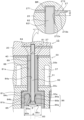
上面にウエハ載置面を有するセラミック基材と、
前記セラミック基材に埋設された電極と、
前記セラミック基材の下面から前記セラミック基材に挿入され、前記電極に設けられた貫通孔を貫通する接合端子と、
前記貫通孔の周縁に前記電極よりも厚くなるように設けられ、内周面が前記接合端子の側面に接合された電極取出部と、
を備えたものである。
Claims (7)
- 上面にウエハ載置面を有するセラミック基材と、
前記セラミック基材に埋設された電極と、
前記セラミック基材の下面から前記セラミック基材に挿入され、前記電極に設けられた貫通孔を貫通する接合端子と、
前記貫通孔の周縁に前記電極よりも厚くなるように設けられ、内周面が前記接合端子の側面に接合された電極取出部と、
を備え、
前記接合端子は、前記セラミック基材の下面から前記電極を貫通するように設けられた端子穴に挿入され、
前記電極取出部は、前記接合端子の上面と対向する位置に設けられておらず、前記接合端子の側面と対向する位置に設けられている
ウエハ載置台。 - 前記電極取出部は、前記貫通孔の周縁に沿って2つ以上設けられている、
請求項1に記載のウエハ載置台。 - 前記電極取出部は、前記端子穴よりも小径の球欠形状又は円柱形状の導電材の一部を前記端子穴で削り取った形状である、
請求項1又は2に記載のウエハ載置台。 - 前記接合端子は、前記貫通孔の内周面と前記電極取出部の内周面とを含む前記端子穴の側面及び前記端子穴の底面と金属ろう材層を介して接合され、
前記金属ろう材層は、前記セラミック基材の下面に達しないように設けられている、
請求項3に記載のウエハ載置台。 - 前記電極取出部の前記内周面は、前記ウエハ載置面に対して垂直な面である、
請求項1~4のいずれか1項に記載のウエハ載置台。 - 前記電極取出部の前記内周面側の厚みは、0.1mm以上1mm以下である、
請求項1~5のいずれか1項に記載のウエハ載置台。 - 前記電極取出部は、前記電極に対して下向きに凸になっている、
請求項1~6のいずれか1項に記載のウエハ載置台。
Priority Applications (5)
| Application Number | Priority Date | Filing Date | Title |
|---|---|---|---|
| JP2022002885A JP7623309B2 (ja) | 2022-01-12 | 2022-01-12 | ウエハ載置台 |
| CN202211257455.2A CN116469744B (zh) | 2022-01-12 | 2022-10-14 | 晶片载放台 |
| US18/056,333 US12300476B2 (en) | 2022-01-12 | 2022-11-17 | Wafer placement table |
| KR1020220155375A KR102863907B1 (ko) | 2022-01-12 | 2022-11-18 | 웨이퍼 배치대 |
| TW112100533A TWI885314B (zh) | 2022-01-12 | 2023-01-06 | 晶圓載置台 |
Applications Claiming Priority (1)
| Application Number | Priority Date | Filing Date | Title |
|---|---|---|---|
| JP2022002885A JP7623309B2 (ja) | 2022-01-12 | 2022-01-12 | ウエハ載置台 |
Publications (2)
| Publication Number | Publication Date |
|---|---|
| JP2023102415A JP2023102415A (ja) | 2023-07-25 |
| JP7623309B2 true JP7623309B2 (ja) | 2025-01-28 |
Family
ID=87068929
Family Applications (1)
| Application Number | Title | Priority Date | Filing Date |
|---|---|---|---|
| JP2022002885A Active JP7623309B2 (ja) | 2022-01-12 | 2022-01-12 | ウエハ載置台 |
Country Status (5)
| Country | Link |
|---|---|
| US (1) | US12300476B2 (ja) |
| JP (1) | JP7623309B2 (ja) |
| KR (1) | KR102863907B1 (ja) |
| CN (1) | CN116469744B (ja) |
| TW (1) | TWI885314B (ja) |
Families Citing this family (1)
| Publication number | Priority date | Publication date | Assignee | Title |
|---|---|---|---|---|
| CN121773764A (zh) * | 2023-09-04 | 2026-03-31 | 日本碍子株式会社 | 晶片载放台 |
Citations (3)
| Publication number | Priority date | Publication date | Assignee | Title |
|---|---|---|---|---|
| JP2001223248A (ja) | 1999-11-25 | 2001-08-17 | Ibiden Co Ltd | ウエハプローバ及びそれに用いられる検査用ステージ |
| WO2008035395A1 (en) | 2006-09-19 | 2008-03-27 | Creative Technology Corporation | Feeding structure of electrostatic chuck, method for producing the same, and method for regenerating feeding structure of electrostatic chuck |
| WO2021075240A1 (ja) | 2019-10-18 | 2021-04-22 | 京セラ株式会社 | 構造体および加熱装置 |
Family Cites Families (15)
| Publication number | Priority date | Publication date | Assignee | Title |
|---|---|---|---|---|
| JPH09213455A (ja) * | 1996-02-05 | 1997-08-15 | Kyocera Corp | ウエハ保持装置の給電構造 |
| US6151203A (en) * | 1998-12-14 | 2000-11-21 | Applied Materials, Inc. | Connectors for an electrostatic chuck and combination thereof |
| KR100544865B1 (ko) | 1999-06-09 | 2006-01-24 | 이비덴 가부시키가이샤 | 세라믹히터 및 발열체용 도전 페이스트 |
| JP2003158051A (ja) | 1999-06-09 | 2003-05-30 | Ibiden Co Ltd | 半導体製造・検査装置用セラミック基板 |
| JP4454505B2 (ja) * | 2005-01-07 | 2010-04-21 | 京セラ株式会社 | ウェハ支持部材 |
| JP2007258610A (ja) * | 2006-03-24 | 2007-10-04 | Ngk Insulators Ltd | アルミナ焼成体 |
| JP5339162B2 (ja) * | 2011-03-30 | 2013-11-13 | Toto株式会社 | 静電チャック |
| US8908349B2 (en) | 2011-03-31 | 2014-12-09 | Ngk Insulators, Ltd. | Member for semiconductor manufacturing apparatus |
| JP6308871B2 (ja) | 2014-05-28 | 2018-04-11 | 新光電気工業株式会社 | 静電チャック及び半導体・液晶製造装置 |
| JP6201963B2 (ja) * | 2014-11-14 | 2017-09-27 | トヨタ自動車株式会社 | 端子部品 |
| CN111801787B (zh) * | 2018-09-13 | 2023-10-03 | 日本碍子株式会社 | 晶圆载置装置 |
| JP7339753B2 (ja) | 2019-03-22 | 2023-09-06 | 京セラ株式会社 | ウエハ載置構造体、ウエハ載置構造体を用いたウエハ載置装置及び基体構造体 |
| JP6918042B2 (ja) * | 2019-03-26 | 2021-08-11 | 日本碍子株式会社 | ウエハ載置装置 |
| JP7362400B2 (ja) * | 2019-10-01 | 2023-10-17 | 東京エレクトロン株式会社 | 載置台及びプラズマ処理装置 |
| JP7797762B2 (ja) * | 2021-08-25 | 2026-01-14 | 新光電気工業株式会社 | 基板固定装置 |
-
2022
- 2022-01-12 JP JP2022002885A patent/JP7623309B2/ja active Active
- 2022-10-14 CN CN202211257455.2A patent/CN116469744B/zh active Active
- 2022-11-17 US US18/056,333 patent/US12300476B2/en active Active
- 2022-11-18 KR KR1020220155375A patent/KR102863907B1/ko active Active
-
2023
- 2023-01-06 TW TW112100533A patent/TWI885314B/zh active
Patent Citations (3)
| Publication number | Priority date | Publication date | Assignee | Title |
|---|---|---|---|---|
| JP2001223248A (ja) | 1999-11-25 | 2001-08-17 | Ibiden Co Ltd | ウエハプローバ及びそれに用いられる検査用ステージ |
| WO2008035395A1 (en) | 2006-09-19 | 2008-03-27 | Creative Technology Corporation | Feeding structure of electrostatic chuck, method for producing the same, and method for regenerating feeding structure of electrostatic chuck |
| WO2021075240A1 (ja) | 2019-10-18 | 2021-04-22 | 京セラ株式会社 | 構造体および加熱装置 |
Also Published As
| Publication number | Publication date |
|---|---|
| CN116469744B (zh) | 2026-01-16 |
| TWI885314B (zh) | 2025-06-01 |
| TW202329320A (zh) | 2023-07-16 |
| US20230223245A1 (en) | 2023-07-13 |
| KR102863907B1 (ko) | 2025-09-23 |
| JP2023102415A (ja) | 2023-07-25 |
| KR20230109080A (ko) | 2023-07-19 |
| CN116469744A (zh) | 2023-07-21 |
| US12300476B2 (en) | 2025-05-13 |
Similar Documents
| Publication | Publication Date | Title |
|---|---|---|
| JP7620593B2 (ja) | ウエハ載置台 | |
| US12374534B2 (en) | Member for semiconductor manufacturing apparatus | |
| KR20230053499A (ko) | 웨이퍼 배치대 | |
| US12308220B2 (en) | Wafer placement table | |
| KR102755203B1 (ko) | 웨이퍼 배치대 | |
| JP7623309B2 (ja) | ウエハ載置台 | |
| CN115995374B (zh) | 晶片载放台 | |
| JP2025109922A (ja) | ウエハ載置台 | |
| JP7637227B2 (ja) | ウエハ載置台 | |
| JP7526349B2 (ja) | ウエハ載置台 | |
| JP7675282B1 (ja) | ウエハ載置台 | |
| JP7621458B2 (ja) | ウエハ載置台 | |
| JP7606598B2 (ja) | ウエハ載置台 | |
| KR20260057603A (ko) | 웨이퍼 배치대 |
Legal Events
| Date | Code | Title | Description |
|---|---|---|---|
| A621 | Written request for application examination |
Free format text: JAPANESE INTERMEDIATE CODE: A621 Effective date: 20231020 |
|
| A977 | Report on retrieval |
Free format text: JAPANESE INTERMEDIATE CODE: A971007 Effective date: 20240731 |
|
| A131 | Notification of reasons for refusal |
Free format text: JAPANESE INTERMEDIATE CODE: A131 Effective date: 20240820 |
|
| A521 | Request for written amendment filed |
Free format text: JAPANESE INTERMEDIATE CODE: A523 Effective date: 20240913 |
|
| TRDD | Decision of grant or rejection written | ||
| A01 | Written decision to grant a patent or to grant a registration (utility model) |
Free format text: JAPANESE INTERMEDIATE CODE: A01 Effective date: 20250107 |
|
| A61 | First payment of annual fees (during grant procedure) |
Free format text: JAPANESE INTERMEDIATE CODE: A61 Effective date: 20250116 |
|
| R150 | Certificate of patent or registration of utility model |
Ref document number: 7623309 Country of ref document: JP Free format text: JAPANESE INTERMEDIATE CODE: R150 |