JP7625732B2 - 表示装置、情報表示装置、及び電子機器 - Google Patents
表示装置、情報表示装置、及び電子機器 Download PDFInfo
- Publication number
- JP7625732B2 JP7625732B2 JP2024006075A JP2024006075A JP7625732B2 JP 7625732 B2 JP7625732 B2 JP 7625732B2 JP 2024006075 A JP2024006075 A JP 2024006075A JP 2024006075 A JP2024006075 A JP 2024006075A JP 7625732 B2 JP7625732 B2 JP 7625732B2
- Authority
- JP
- Japan
- Prior art keywords
- light
- signal
- display device
- signal line
- emitting element
- Prior art date
- Legal status (The legal status is an assumption and is not a legal conclusion. Google has not performed a legal analysis and makes no representation as to the accuracy of the status listed.)
- Active
Links
Images





Classifications
-
- G—PHYSICS
- G09—EDUCATION; CRYPTOGRAPHY; DISPLAY; ADVERTISING; SEALS
- G09G—ARRANGEMENTS OR CIRCUITS FOR CONTROL OF INDICATING DEVICES USING STATIC MEANS TO PRESENT VARIABLE INFORMATION
- G09G3/00—Control arrangements or circuits, of interest only in connection with visual indicators other than cathode-ray tubes
- G09G3/20—Control arrangements or circuits, of interest only in connection with visual indicators other than cathode-ray tubes for presentation of an assembly of a number of characters, e.g. a page, by composing the assembly by combination of individual elements arranged in a matrix no fixed position being assigned to or needed to be assigned to the individual characters or partial characters
- G09G3/22—Control arrangements or circuits, of interest only in connection with visual indicators other than cathode-ray tubes for presentation of an assembly of a number of characters, e.g. a page, by composing the assembly by combination of individual elements arranged in a matrix no fixed position being assigned to or needed to be assigned to the individual characters or partial characters using controlled light sources
- G09G3/30—Control arrangements or circuits, of interest only in connection with visual indicators other than cathode-ray tubes for presentation of an assembly of a number of characters, e.g. a page, by composing the assembly by combination of individual elements arranged in a matrix no fixed position being assigned to or needed to be assigned to the individual characters or partial characters using controlled light sources using electroluminescent panels
- G09G3/32—Control arrangements or circuits, of interest only in connection with visual indicators other than cathode-ray tubes for presentation of an assembly of a number of characters, e.g. a page, by composing the assembly by combination of individual elements arranged in a matrix no fixed position being assigned to or needed to be assigned to the individual characters or partial characters using controlled light sources using electroluminescent panels semiconductive, e.g. using light-emitting diodes [LED]
- G09G3/3208—Control arrangements or circuits, of interest only in connection with visual indicators other than cathode-ray tubes for presentation of an assembly of a number of characters, e.g. a page, by composing the assembly by combination of individual elements arranged in a matrix no fixed position being assigned to or needed to be assigned to the individual characters or partial characters using controlled light sources using electroluminescent panels semiconductive, e.g. using light-emitting diodes [LED] organic, e.g. using organic light-emitting diodes [OLED]
- G09G3/3225—Control arrangements or circuits, of interest only in connection with visual indicators other than cathode-ray tubes for presentation of an assembly of a number of characters, e.g. a page, by composing the assembly by combination of individual elements arranged in a matrix no fixed position being assigned to or needed to be assigned to the individual characters or partial characters using controlled light sources using electroluminescent panels semiconductive, e.g. using light-emitting diodes [LED] organic, e.g. using organic light-emitting diodes [OLED] using an active matrix
- G09G3/3233—Control arrangements or circuits, of interest only in connection with visual indicators other than cathode-ray tubes for presentation of an assembly of a number of characters, e.g. a page, by composing the assembly by combination of individual elements arranged in a matrix no fixed position being assigned to or needed to be assigned to the individual characters or partial characters using controlled light sources using electroluminescent panels semiconductive, e.g. using light-emitting diodes [LED] organic, e.g. using organic light-emitting diodes [OLED] using an active matrix with pixel circuitry controlling the current through the light-emitting element
-
- G—PHYSICS
- G06—COMPUTING OR CALCULATING; COUNTING
- G06F—ELECTRIC DIGITAL DATA PROCESSING
- G06F3/00—Input arrangements for transferring data to be processed into a form capable of being handled by the computer; Output arrangements for transferring data from processing unit to output unit, e.g. interface arrangements
- G06F3/01—Input arrangements or combined input and output arrangements for interaction between user and computer
- G06F3/011—Arrangements for interaction with the human body, e.g. for user immersion in virtual reality
- G06F3/013—Eye tracking input arrangements
-
- G—PHYSICS
- G09—EDUCATION; CRYPTOGRAPHY; DISPLAY; ADVERTISING; SEALS
- G09G—ARRANGEMENTS OR CIRCUITS FOR CONTROL OF INDICATING DEVICES USING STATIC MEANS TO PRESENT VARIABLE INFORMATION
- G09G3/00—Control arrangements or circuits, of interest only in connection with visual indicators other than cathode-ray tubes
- G09G3/20—Control arrangements or circuits, of interest only in connection with visual indicators other than cathode-ray tubes for presentation of an assembly of a number of characters, e.g. a page, by composing the assembly by combination of individual elements arranged in a matrix no fixed position being assigned to or needed to be assigned to the individual characters or partial characters
- G09G3/22—Control arrangements or circuits, of interest only in connection with visual indicators other than cathode-ray tubes for presentation of an assembly of a number of characters, e.g. a page, by composing the assembly by combination of individual elements arranged in a matrix no fixed position being assigned to or needed to be assigned to the individual characters or partial characters using controlled light sources
- G09G3/30—Control arrangements or circuits, of interest only in connection with visual indicators other than cathode-ray tubes for presentation of an assembly of a number of characters, e.g. a page, by composing the assembly by combination of individual elements arranged in a matrix no fixed position being assigned to or needed to be assigned to the individual characters or partial characters using controlled light sources using electroluminescent panels
- G09G3/32—Control arrangements or circuits, of interest only in connection with visual indicators other than cathode-ray tubes for presentation of an assembly of a number of characters, e.g. a page, by composing the assembly by combination of individual elements arranged in a matrix no fixed position being assigned to or needed to be assigned to the individual characters or partial characters using controlled light sources using electroluminescent panels semiconductive, e.g. using light-emitting diodes [LED]
- G09G3/3208—Control arrangements or circuits, of interest only in connection with visual indicators other than cathode-ray tubes for presentation of an assembly of a number of characters, e.g. a page, by composing the assembly by combination of individual elements arranged in a matrix no fixed position being assigned to or needed to be assigned to the individual characters or partial characters using controlled light sources using electroluminescent panels semiconductive, e.g. using light-emitting diodes [LED] organic, e.g. using organic light-emitting diodes [OLED]
- G09G3/3275—Details of drivers for data electrodes
-
- G—PHYSICS
- G09—EDUCATION; CRYPTOGRAPHY; DISPLAY; ADVERTISING; SEALS
- G09G—ARRANGEMENTS OR CIRCUITS FOR CONTROL OF INDICATING DEVICES USING STATIC MEANS TO PRESENT VARIABLE INFORMATION
- G09G2300/00—Aspects of the constitution of display devices
- G09G2300/08—Active matrix structure, i.e. with use of active elements, inclusive of non-linear two terminal elements, in the pixels together with light emitting or modulating elements
- G09G2300/0809—Several active elements per pixel in active matrix panels
- G09G2300/0819—Several active elements per pixel in active matrix panels used for counteracting undesired variations, e.g. feedback or autozeroing
-
- G—PHYSICS
- G09—EDUCATION; CRYPTOGRAPHY; DISPLAY; ADVERTISING; SEALS
- G09G—ARRANGEMENTS OR CIRCUITS FOR CONTROL OF INDICATING DEVICES USING STATIC MEANS TO PRESENT VARIABLE INFORMATION
- G09G2300/00—Aspects of the constitution of display devices
- G09G2300/08—Active matrix structure, i.e. with use of active elements, inclusive of non-linear two terminal elements, in the pixels together with light emitting or modulating elements
- G09G2300/0809—Several active elements per pixel in active matrix panels
- G09G2300/0842—Several active elements per pixel in active matrix panels forming a memory circuit, e.g. a dynamic memory with one capacitor
- G09G2300/0847—Several active elements per pixel in active matrix panels forming a memory circuit, e.g. a dynamic memory with one capacitor being a dynamic memory without any storage capacitor, i.e. with use of parasitic capacitances as storage elements
-
- G—PHYSICS
- G09—EDUCATION; CRYPTOGRAPHY; DISPLAY; ADVERTISING; SEALS
- G09G—ARRANGEMENTS OR CIRCUITS FOR CONTROL OF INDICATING DEVICES USING STATIC MEANS TO PRESENT VARIABLE INFORMATION
- G09G2300/00—Aspects of the constitution of display devices
- G09G2300/08—Active matrix structure, i.e. with use of active elements, inclusive of non-linear two terminal elements, in the pixels together with light emitting or modulating elements
- G09G2300/0809—Several active elements per pixel in active matrix panels
- G09G2300/0842—Several active elements per pixel in active matrix panels forming a memory circuit, e.g. a dynamic memory with one capacitor
- G09G2300/0852—Several active elements per pixel in active matrix panels forming a memory circuit, e.g. a dynamic memory with one capacitor being a dynamic memory with more than one capacitor
-
- G—PHYSICS
- G09—EDUCATION; CRYPTOGRAPHY; DISPLAY; ADVERTISING; SEALS
- G09G—ARRANGEMENTS OR CIRCUITS FOR CONTROL OF INDICATING DEVICES USING STATIC MEANS TO PRESENT VARIABLE INFORMATION
- G09G2310/00—Command of the display device
- G09G2310/02—Addressing, scanning or driving the display screen or processing steps related thereto
- G09G2310/0264—Details of driving circuits
- G09G2310/0297—Special arrangements with multiplexing or demultiplexing of display data in the drivers for data electrodes, in a pre-processing circuitry delivering display data to said drivers or in the matrix panel, e.g. multiplexing plural data signals to one D/A converter or demultiplexing the D/A converter output to multiple columns
-
- G—PHYSICS
- G09—EDUCATION; CRYPTOGRAPHY; DISPLAY; ADVERTISING; SEALS
- G09G—ARRANGEMENTS OR CIRCUITS FOR CONTROL OF INDICATING DEVICES USING STATIC MEANS TO PRESENT VARIABLE INFORMATION
- G09G2320/00—Control of display operating conditions
- G09G2320/02—Improving the quality of display appearance
- G09G2320/0233—Improving the luminance or brightness uniformity across the screen
-
- G—PHYSICS
- G09—EDUCATION; CRYPTOGRAPHY; DISPLAY; ADVERTISING; SEALS
- G09G—ARRANGEMENTS OR CIRCUITS FOR CONTROL OF INDICATING DEVICES USING STATIC MEANS TO PRESENT VARIABLE INFORMATION
- G09G3/00—Control arrangements or circuits, of interest only in connection with visual indicators other than cathode-ray tubes
- G09G3/20—Control arrangements or circuits, of interest only in connection with visual indicators other than cathode-ray tubes for presentation of an assembly of a number of characters, e.g. a page, by composing the assembly by combination of individual elements arranged in a matrix no fixed position being assigned to or needed to be assigned to the individual characters or partial characters
- G09G3/22—Control arrangements or circuits, of interest only in connection with visual indicators other than cathode-ray tubes for presentation of an assembly of a number of characters, e.g. a page, by composing the assembly by combination of individual elements arranged in a matrix no fixed position being assigned to or needed to be assigned to the individual characters or partial characters using controlled light sources
- G09G3/30—Control arrangements or circuits, of interest only in connection with visual indicators other than cathode-ray tubes for presentation of an assembly of a number of characters, e.g. a page, by composing the assembly by combination of individual elements arranged in a matrix no fixed position being assigned to or needed to be assigned to the individual characters or partial characters using controlled light sources using electroluminescent panels
- G09G3/32—Control arrangements or circuits, of interest only in connection with visual indicators other than cathode-ray tubes for presentation of an assembly of a number of characters, e.g. a page, by composing the assembly by combination of individual elements arranged in a matrix no fixed position being assigned to or needed to be assigned to the individual characters or partial characters using controlled light sources using electroluminescent panels semiconductive, e.g. using light-emitting diodes [LED]
- G09G3/3208—Control arrangements or circuits, of interest only in connection with visual indicators other than cathode-ray tubes for presentation of an assembly of a number of characters, e.g. a page, by composing the assembly by combination of individual elements arranged in a matrix no fixed position being assigned to or needed to be assigned to the individual characters or partial characters using controlled light sources using electroluminescent panels semiconductive, e.g. using light-emitting diodes [LED] organic, e.g. using organic light-emitting diodes [OLED]
- G09G3/3225—Control arrangements or circuits, of interest only in connection with visual indicators other than cathode-ray tubes for presentation of an assembly of a number of characters, e.g. a page, by composing the assembly by combination of individual elements arranged in a matrix no fixed position being assigned to or needed to be assigned to the individual characters or partial characters using controlled light sources using electroluminescent panels semiconductive, e.g. using light-emitting diodes [LED] organic, e.g. using organic light-emitting diodes [OLED] using an active matrix
-
- H—ELECTRICITY
- H10—SEMICONDUCTOR DEVICES; ELECTRIC SOLID-STATE DEVICES NOT OTHERWISE PROVIDED FOR
- H10K—ORGANIC ELECTRIC SOLID-STATE DEVICES
- H10K59/00—Integrated devices, or assemblies of multiple devices, comprising at least one organic light-emitting element covered by group H10K50/00
- H10K59/60—OLEDs integrated with inorganic light-sensitive elements, e.g. with inorganic solar cells or inorganic photodiodes
- H10K59/65—OLEDs integrated with inorganic image sensors
Landscapes
- Engineering & Computer Science (AREA)
- Theoretical Computer Science (AREA)
- Physics & Mathematics (AREA)
- General Physics & Mathematics (AREA)
- Computer Hardware Design (AREA)
- General Engineering & Computer Science (AREA)
- Human Computer Interaction (AREA)
- Control Of El Displays (AREA)
- Control Of Indicators Other Than Cathode Ray Tubes (AREA)
- Electroluminescent Light Sources (AREA)
- Devices For Indicating Variable Information By Combining Individual Elements (AREA)
Description
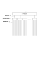
本実施形態に係る表示装置について図面を参照して説明する。
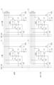
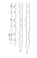
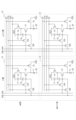
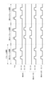
図5に、本実施形態の画素回路を示す。第1の実施形態と異なるのは、1フレーム期間のある行において、画像信号を供給する信号線が異なる画素が存在する点である。すなわち、任意の1フレームのある1行において、信号電圧(画像信号)を供給する信号線24が、信号線24Aの画素と信号線24Bの画素が存在する。
図6を用いて本実施形態の画素回路を示す。
図8を用いて本実施形態の画素回路を示す。
[有機発光素子の構成]
有機発光素子は、基板の上に、陽極、有機化合物層、陰極を形成して設けられる。陰極の上には、保護層、カラーフィルタ等を設けてよい。カラーフィルタを設ける場合は、保護層との間に平坦化層を設けてよい。平坦化層はアクリル樹脂等で構成することができる。
基板は、石英、ガラス、シリコンウエハ、樹脂、金属等が挙げられる。また、基板上には、トランジスタなどのスイッチング素子や配線を備え、その上に絶縁層を備えてもよい。絶縁層としては、陽極2と配線の導通を確保するために、コンタクトホールを形成可能で、かつ接続しない配線との絶縁を確保できれば、材料は問わない。例えば、ポリイミド等の樹脂、酸化シリコン、窒化シリコンなどを用いることができる。
電極は、一対の電極を用いることができる。一対の電極は、陽極と陰極であってよい。有機発光素子が発光する方向に電界を印加する場合に、電位が高い電極が陽極であり、他方が陰極である。また、発光層にホールを供給する電極が陽極であり、電子を供給する電極が陰極であるということもできる。
陰極の上に、保護層を設けてもよい。例えば、陰極上に吸湿剤を設けたガラスを接着することで、有機化合物層に対する水等の浸入を抑え、表示不良の発生を抑えることができる。また、別の実施形態としては、陰極上に窒化ケイ素等のパッシベーション膜を設け、有機EL層に対する水等の浸入を抑えてもよい。例えば、陰極7形成後に真空を破らずに別のチャンバーに搬送し、CVD法で厚さ2μmの窒化ケイ素膜を形成することで、保護層としてもよい。CVD法の成膜の後で原子堆積法(ALD法)を用いた保護層を設けてもよい。
保護層の上にカラーフィルタを設けてもよい。例えば、有機発光素子のサイズを考慮したカラーフィルタを別の基板上に設け、それと有機発光素子を設けた基板と貼り合わせてもよいし、上記で示した保護層上にフォトリソグラフィ技術を用いて、カラーフィルタをパターニングしてもよい。カラーフィルタは、高分子で構成されてよい。
カラーフィルタと保護層との間に平坦化層を有してもよい。平坦化層は有機化合物で構成されてよく、低分子であっても、高分子であってもよいが、高分子であることが好ましい。
平坦化層の上には、対抗基板を有してよい。対抗基板は、前述の基板と対応する位置に設けられるため、対抗基板と呼ばれる。対抗基板の構成材料は、前述の基板と同じであってよい。
本発明の一実施形態に係る有機発光素子を構成する有機化合物層(正孔注入層、正孔輸送層、電子阻止層、発光層、正孔阻止層、電子輸送層、電子注入層等)は、以下に示す方法により形成される。
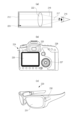
第1乃至第4の実施形態に係る表示装置は各種電子機器の表示部として用いることができる。たとえば、デジタルカメラ、ビデオカメラ、ヘッドマウントディスプレイ(ゴーグル型ディスプレイ)、ゲーム機、カーナビゲーション、パーソナルコンピュータ、携帯情報端末、電子書籍、テレビ受像機等が挙げられる。以下に図面を用いて具体例を説明する。
11 発光素子
21 信号線
Claims (8)
- データ信号出力部と、
前記データ信号出力部に接続されている第1信号線と、
前記データ信号出力部に接続され、前記第1信号線とは異なる第2信号線と、
第1発光素子と、
ゲートを含み、前記第1発光素子にソースまたはドレインのいずれかが接続された第1トランジスタと、
前記第1信号線と前記ゲートとの間に接続された第2トランジスタと、
前記第2信号線と前記ゲートとの間に接続された第3トランジスタと、を有する表示装置であって、
前記第1信号線、前記第2信号線のいずれも、画像信号が入力可能に構成されており、
所定の行において、
第1のフレーム期間において、前記第1信号線に前記画像信号が入力されている状態で、前記第2トランジスタがオンになり、前記第1のフレーム期間の全期間で前記第3トランジスタはオフに維持されており、
前記第1のフレーム期間の次の第2のフレーム期間において、前記第2信号線に前記画像信号が入力されている状態で、前記第3トランジスタがオンになり、前記第2のフレーム期間の全期間で前記第2トランジスタはオフに維持されていることを特徴とする表示装置。 - 前記第1信号線の寄生容量が、前記第2信号線の寄生容量と異なることを特徴とする請求項1に記載の表示装置。
- 前記データ信号出力部に接続されている第3信号線と、
第2発光素子と、
ゲートを含み、前記第2発光素子にソースまたはドレインのいずれかが接続された第4トランジスタと、
前記第3信号線と前記第2発光素子の前記ゲートとの間に接続された第5トランジスタと、を有し、
前記第2発光素子の前記ゲートは、前記第3信号線からのみ信号が入力されることを特徴とする請求項1または2に記載の表示装置。 - 前記第1発光素子と前記第2発光素子とは、発光色が異なることを特徴とする請求項3に記載の表示装置。
- 前記第2発光素子は青発光素子であることを特徴とする請求項4に記載の表示装置。
- 撮像素子と、
請求項1乃至5のいずれか1項に記載の表示装置と、を有し、
前記撮像素子からのユーザーの視線情報に基づいて前記表示装置の表示画像を制御する情報表示装置。 - 複数のレンズを有する光学部と、前記光学部を通過した光を受光する撮像素子と、前記撮像素子が撮像した画像を表示する表示部と、を有し、
前記表示部は請求項1乃至5のいずれか1項に記載の表示装置を有することを特徴とする光電変換装置。 - 請求項1乃至5のいずれか1項に記載の表示装置を有する表示部と、前記表示部が設けられた筐体と、前記筐体に設けられ、外部と通信する通信部と、を有することを特徴とする電子機器。
Priority Applications (1)
| Application Number | Priority Date | Filing Date | Title |
|---|---|---|---|
| JP2024006075A JP7625732B2 (ja) | 2019-10-30 | 2024-01-18 | 表示装置、情報表示装置、及び電子機器 |
Applications Claiming Priority (2)
| Application Number | Priority Date | Filing Date | Title |
|---|---|---|---|
| JP2019198013A JP2021071593A (ja) | 2019-10-30 | 2019-10-30 | 表示装置、情報表示装置、及び電子機器 |
| JP2024006075A JP7625732B2 (ja) | 2019-10-30 | 2024-01-18 | 表示装置、情報表示装置、及び電子機器 |
Related Parent Applications (1)
| Application Number | Title | Priority Date | Filing Date |
|---|---|---|---|
| JP2019198013A Division JP2021071593A (ja) | 2019-10-30 | 2019-10-30 | 表示装置、情報表示装置、及び電子機器 |
Publications (2)
| Publication Number | Publication Date |
|---|---|
| JP2024032811A JP2024032811A (ja) | 2024-03-12 |
| JP7625732B2 true JP7625732B2 (ja) | 2025-02-03 |
Family
ID=75648921
Family Applications (2)
| Application Number | Title | Priority Date | Filing Date |
|---|---|---|---|
| JP2019198013A Pending JP2021071593A (ja) | 2019-10-30 | 2019-10-30 | 表示装置、情報表示装置、及び電子機器 |
| JP2024006075A Active JP7625732B2 (ja) | 2019-10-30 | 2024-01-18 | 表示装置、情報表示装置、及び電子機器 |
Family Applications Before (1)
| Application Number | Title | Priority Date | Filing Date |
|---|---|---|---|
| JP2019198013A Pending JP2021071593A (ja) | 2019-10-30 | 2019-10-30 | 表示装置、情報表示装置、及び電子機器 |
Country Status (3)
| Country | Link |
|---|---|
| US (1) | US11521557B2 (ja) |
| JP (2) | JP2021071593A (ja) |
| CN (1) | CN112750403B (ja) |
Families Citing this family (4)
| Publication number | Priority date | Publication date | Assignee | Title |
|---|---|---|---|---|
| JP7541820B2 (ja) * | 2019-11-01 | 2024-08-29 | キヤノン株式会社 | 有機化合物及び有機発光素子 |
| GB202008691D0 (en) * | 2020-06-09 | 2020-07-22 | Ams Int Ag | Ambient light sensing |
| US12424600B1 (en) * | 2022-11-07 | 2025-09-23 | Meta Platforms Technologies, Llc | Tiled display system for field of view expansion |
| CN117079566A (zh) * | 2022-12-26 | 2023-11-17 | 天马新型显示技术研究院(厦门)有限公司 | 一种显示面板和显示装置 |
Citations (4)
| Publication number | Priority date | Publication date | Assignee | Title |
|---|---|---|---|---|
| JP2002278478A (ja) | 2000-12-21 | 2002-09-27 | Semiconductor Energy Lab Co Ltd | 発光装置、発光装置の駆動方法及び電子機器 |
| US20080316149A1 (en) | 2006-12-29 | 2008-12-25 | In Hwan Kim | Electro-luminescence pixel, panel with the pixel, and device and method for driving the panel |
| JP2010113231A (ja) | 2008-11-07 | 2010-05-20 | Sony Corp | 表示装置及びその駆動方法と電子機器 |
| JP2015132817A (ja) | 2013-12-10 | 2015-07-23 | 株式会社半導体エネルギー研究所 | 発光装置 |
Family Cites Families (28)
| Publication number | Priority date | Publication date | Assignee | Title |
|---|---|---|---|---|
| JP3723507B2 (ja) * | 2002-01-29 | 2005-12-07 | 三洋電機株式会社 | 駆動回路 |
| TW587395B (en) * | 2002-05-28 | 2004-05-11 | Ritdisplay Corp | Full color organic light-emitting display device |
| KR20050080318A (ko) | 2004-02-09 | 2005-08-12 | 삼성전자주식회사 | 트랜지스터의 구동 방법과, 이를 이용한 구동소자,표시패널 및 표시장치 |
| KR101057275B1 (ko) * | 2004-09-24 | 2011-08-16 | 엘지디스플레이 주식회사 | 유기발광소자 |
| WO2006059737A1 (en) | 2004-11-30 | 2006-06-08 | Semiconductor Energy Laboratory Co., Ltd. | Display device and driving method thereof, semiconductor device, and electronic apparatus |
| JP5264014B2 (ja) | 2004-11-30 | 2013-08-14 | 株式会社半導体エネルギー研究所 | 半導体装置、表示装置及び電子機器 |
| JP5121118B2 (ja) | 2004-12-08 | 2013-01-16 | 株式会社ジャパンディスプレイイースト | 表示装置 |
| JP5177953B2 (ja) | 2005-01-21 | 2013-04-10 | 株式会社半導体エネルギー研究所 | 半導体装置及び表示装置 |
| US7646367B2 (en) | 2005-01-21 | 2010-01-12 | Semiconductor Energy Laboratory Co., Ltd. | Semiconductor device, display device and electronic apparatus |
| FR2882457B1 (fr) | 2005-02-21 | 2007-09-21 | Commissariat Energie Atomique | Circuit d'adressage de pixels et procede de controle d'un tel circuit |
| JP2009015276A (ja) | 2007-06-05 | 2009-01-22 | Sony Corp | El表示パネル駆動方法、el表示パネル、el表示パネル駆動装置及び電子機器 |
| KR101407302B1 (ko) * | 2007-12-27 | 2014-06-13 | 엘지디스플레이 주식회사 | 발광 표시 장치 및 그 구동 방법 |
| EP2239723B1 (en) | 2008-02-08 | 2015-01-28 | Sharp Kabushiki Kaisha | Pixel circuit and display device |
| US8229153B2 (en) * | 2008-04-01 | 2012-07-24 | Apple Inc. | Microphone packaging in a mobile communications device |
| US20090251780A1 (en) * | 2008-04-02 | 2009-10-08 | Panasonic Corporation | Zoom lens system, interchangeable lens apparatus and camera system |
| JP2011112723A (ja) * | 2009-11-24 | 2011-06-09 | Sony Corp | 表示装置およびその駆動方法ならびに電子機器 |
| US8531394B2 (en) * | 2010-07-23 | 2013-09-10 | Gregory A. Maltz | Unitized, vision-controlled, wireless eyeglasses transceiver |
| KR101859474B1 (ko) * | 2011-09-05 | 2018-05-23 | 엘지디스플레이 주식회사 | 유기 발광 다이오드 표시 장치의 화소 회로 |
| JP6128738B2 (ja) * | 2012-02-28 | 2017-05-17 | キヤノン株式会社 | 画素回路及びその駆動方法 |
| WO2013172220A1 (en) * | 2012-05-18 | 2013-11-21 | Semiconductor Energy Laboratory Co., Ltd. | Pixel circuit, display device, and electronic device |
| KR101411619B1 (ko) * | 2012-09-27 | 2014-06-25 | 엘지디스플레이 주식회사 | 화소 회로와 그 구동 방법 및 이를 이용한 유기 발광 표시 장치 |
| JP6201465B2 (ja) * | 2013-07-08 | 2017-09-27 | ソニー株式会社 | 表示装置、表示装置の駆動方法、及び、電子機器 |
| KR102237748B1 (ko) * | 2014-11-24 | 2021-04-12 | 삼성디스플레이 주식회사 | 유기 발광 표시 장치 및 이의 구동방법 |
| CN104934008A (zh) * | 2015-07-09 | 2015-09-23 | 京东方科技集团股份有限公司 | 一种阵列基板及其驱动方法、显示面板、显示装置 |
| JP2018045186A (ja) | 2016-09-16 | 2018-03-22 | 株式会社ジャパンディスプレイ | 表示装置 |
| US10332443B2 (en) * | 2017-02-03 | 2019-06-25 | Abl Ip Holding Llc | Luminaire and lighting system, combining transparent lighting device and display coupled to output image via the transparent lighting device |
| CN109841189B (zh) * | 2017-11-29 | 2020-08-14 | 京东方科技集团股份有限公司 | 像素电路及其驱动方法、显示面板和显示装置 |
| KR102550867B1 (ko) * | 2018-12-28 | 2023-07-04 | 엘지디스플레이 주식회사 | 발광표시장치, 발광표시패널, 구동회로 및 구동방법 |
-
2019
- 2019-10-30 JP JP2019198013A patent/JP2021071593A/ja active Pending
-
2020
- 2020-10-28 US US17/083,105 patent/US11521557B2/en active Active
- 2020-10-29 CN CN202011179835.XA patent/CN112750403B/zh active Active
-
2024
- 2024-01-18 JP JP2024006075A patent/JP7625732B2/ja active Active
Patent Citations (4)
| Publication number | Priority date | Publication date | Assignee | Title |
|---|---|---|---|---|
| JP2002278478A (ja) | 2000-12-21 | 2002-09-27 | Semiconductor Energy Lab Co Ltd | 発光装置、発光装置の駆動方法及び電子機器 |
| US20080316149A1 (en) | 2006-12-29 | 2008-12-25 | In Hwan Kim | Electro-luminescence pixel, panel with the pixel, and device and method for driving the panel |
| JP2010113231A (ja) | 2008-11-07 | 2010-05-20 | Sony Corp | 表示装置及びその駆動方法と電子機器 |
| JP2015132817A (ja) | 2013-12-10 | 2015-07-23 | 株式会社半導体エネルギー研究所 | 発光装置 |
Also Published As
| Publication number | Publication date |
|---|---|
| US11521557B2 (en) | 2022-12-06 |
| CN112750403B (zh) | 2025-08-12 |
| JP2021071593A (ja) | 2021-05-06 |
| JP2024032811A (ja) | 2024-03-12 |
| US20210134231A1 (en) | 2021-05-06 |
| CN112750403A (zh) | 2021-05-04 |
Similar Documents
| Publication | Publication Date | Title |
|---|---|---|
| US11087680B2 (en) | Display device, image capturing device, illumination device, mobile body, and electronic apparatus | |
| JP7625732B2 (ja) | 表示装置、情報表示装置、及び電子機器 | |
| JP7523639B2 (ja) | 発光装置、表示装置、光電変換装置、電子機器、照明装置および移動体 | |
| CN111223450B (zh) | 显示设备、图像捕获设备、照明设备、移动体和电子装置 | |
| JP7397694B2 (ja) | 発光装置、撮像装置、電子機器及び移動体 | |
| JP7641746B2 (ja) | 発光装置、光電変換装置、電子機器、照明装置及び移動体 | |
| US12154492B2 (en) | Light emitting device, display device, photoelectric conversion device, electronic apparatus, illumination device, and moving body | |
| JP7500212B2 (ja) | 発光装置、表示撮像装置、及び電子機器 | |
| JP2023026092A (ja) | 発光装置、光電変換装置、電子機器、照明装置および移動体 | |
| US12482421B2 (en) | Display device having driving transistor to drive electro-optical element | |
| US12437716B2 (en) | Light emitting device, display device, photoelectric conversion device, electronic apparatus, and wearable device | |
| JP2024154367A (ja) | 表示装置、表示装置の駆動方法 | |
| EP4646079A1 (en) | Display device, photoelectric conversion device, and electronic apparatus | |
| US12615935B2 (en) | Light emitting apparatus, display apparatus, photoelectric conversion apparatus, electronic device, illumination apparatus, and moving body | |
| US20250294993A1 (en) | Light-emitting apparatus | |
| US20250048838A1 (en) | Light emitting device, display device, photoelectric conversion device, electronic apparatus, and manufacturing method of light emitting device | |
| JP2024081574A (ja) | 発光装置、表示装置、光電変換装置、電子機器、および、ウェアラブルデバイス | |
| WO2024241743A1 (ja) | 発光装置、表示装置、光電変換装置、電子機器、照明装置、および、移動体 | |
| JP2024074234A (ja) | 発光装置、表示装置、光電変換装置、電子機器、照明装置及び移動体 | |
| JP2024131054A (ja) | 発光装置、表示装置、光電変換装置、電子機器、照明装置、および、移動体 | |
| JP2023177215A (ja) | 発光装置、表示装置、光電変換装置、電子機器、および、発光装置の製造方法 |
Legal Events
| Date | Code | Title | Description |
|---|---|---|---|
| A621 | Written request for application examination |
Free format text: JAPANESE INTERMEDIATE CODE: A621 Effective date: 20240216 |
|
| A977 | Report on retrieval |
Free format text: JAPANESE INTERMEDIATE CODE: A971007 Effective date: 20240927 |
|
| A131 | Notification of reasons for refusal |
Free format text: JAPANESE INTERMEDIATE CODE: A131 Effective date: 20241008 |
|
| A521 | Request for written amendment filed |
Free format text: JAPANESE INTERMEDIATE CODE: A523 Effective date: 20241205 |
|
| TRDD | Decision of grant or rejection written | ||
| A01 | Written decision to grant a patent or to grant a registration (utility model) |
Free format text: JAPANESE INTERMEDIATE CODE: A01 Effective date: 20241224 |
|
| A61 | First payment of annual fees (during grant procedure) |
Free format text: JAPANESE INTERMEDIATE CODE: A61 Effective date: 20250122 |
|
| R150 | Certificate of patent or registration of utility model |
Ref document number: 7625732 Country of ref document: JP Free format text: JAPANESE INTERMEDIATE CODE: R150 |