JP7630575B2 - 3d-ic技術を用いて製造するイベントベースビジョンセンサ - Google Patents
3d-ic技術を用いて製造するイベントベースビジョンセンサ Download PDFInfo
- Publication number
- JP7630575B2 JP7630575B2 JP2023145998A JP2023145998A JP7630575B2 JP 7630575 B2 JP7630575 B2 JP 7630575B2 JP 2023145998 A JP2023145998 A JP 2023145998A JP 2023145998 A JP2023145998 A JP 2023145998A JP 7630575 B2 JP7630575 B2 JP 7630575B2
- Authority
- JP
- Japan
- Prior art keywords
- event
- die
- pixel
- wafer
- vision sensor
- Prior art date
- Legal status (The legal status is an assumption and is not a legal conclusion. Google has not performed a legal analysis and makes no representation as to the accuracy of the status listed.)
- Active
Links
Images



Classifications
-
- H—ELECTRICITY
- H04—ELECTRIC COMMUNICATION TECHNIQUE
- H04N—PICTORIAL COMMUNICATION, e.g. TELEVISION
- H04N25/00—Circuitry of solid-state image sensors [SSIS]; Control thereof
- H04N25/47—Image sensors with pixel address output; Event-driven image sensors; Selection of pixels to be read out based on image data
-
- H—ELECTRICITY
- H04—ELECTRIC COMMUNICATION TECHNIQUE
- H04N—PICTORIAL COMMUNICATION, e.g. TELEVISION
- H04N25/00—Circuitry of solid-state image sensors [SSIS]; Control thereof
- H04N25/70—SSIS architectures; Circuits associated therewith
- H04N25/76—Addressed sensors, e.g. MOS or CMOS sensors
- H04N25/77—Pixel circuitry, e.g. memories, A/D converters, pixel amplifiers, shared circuits or shared components
-
- H—ELECTRICITY
- H04—ELECTRIC COMMUNICATION TECHNIQUE
- H04N—PICTORIAL COMMUNICATION, e.g. TELEVISION
- H04N25/00—Circuitry of solid-state image sensors [SSIS]; Control thereof
- H04N25/70—SSIS architectures; Circuits associated therewith
- H04N25/79—Arrangements of circuitry being divided between different or multiple substrates, chips or circuit boards, e.g. stacked image sensors
-
- H—ELECTRICITY
- H10—SEMICONDUCTOR DEVICES; ELECTRIC SOLID-STATE DEVICES NOT OTHERWISE PROVIDED FOR
- H10D—INORGANIC ELECTRIC SEMICONDUCTOR DEVICES
- H10D64/00—Electrodes of devices having potential barriers
- H10D64/20—Electrodes characterised by their shapes, relative sizes or dispositions
- H10D64/27—Electrodes not carrying the current to be rectified, amplified, oscillated or switched, e.g. gates
- H10D64/311—Gate electrodes for field-effect devices
- H10D64/411—Gate electrodes for field-effect devices for FETs
- H10D64/511—Gate electrodes for field-effect devices for FETs for IGFETs
- H10D64/514—Gate electrodes for field-effect devices for FETs for IGFETs characterised by the insulating layers
-
- H—ELECTRICITY
- H10—SEMICONDUCTOR DEVICES; ELECTRIC SOLID-STATE DEVICES NOT OTHERWISE PROVIDED FOR
- H10F—INORGANIC SEMICONDUCTOR DEVICES SENSITIVE TO INFRARED RADIATION, LIGHT, ELECTROMAGNETIC RADIATION OF SHORTER WAVELENGTH OR CORPUSCULAR RADIATION
- H10F39/00—Integrated devices, or assemblies of multiple devices, comprising at least one element covered by group H10F30/00, e.g. radiation detectors comprising photodiode arrays
- H10F39/011—Manufacture or treatment of image sensors covered by group H10F39/12
- H10F39/018—Manufacture or treatment of image sensors covered by group H10F39/12 of hybrid image sensors
-
- H—ELECTRICITY
- H10—SEMICONDUCTOR DEVICES; ELECTRIC SOLID-STATE DEVICES NOT OTHERWISE PROVIDED FOR
- H10F—INORGANIC SEMICONDUCTOR DEVICES SENSITIVE TO INFRARED RADIATION, LIGHT, ELECTROMAGNETIC RADIATION OF SHORTER WAVELENGTH OR CORPUSCULAR RADIATION
- H10F39/00—Integrated devices, or assemblies of multiple devices, comprising at least one element covered by group H10F30/00, e.g. radiation detectors comprising photodiode arrays
- H10F39/80—Constructional details of image sensors
- H10F39/803—Pixels having integrated switching, control, storage or amplification elements
- H10F39/8037—Pixels having integrated switching, control, storage or amplification elements the integrated elements comprising a transistor
- H10F39/80373—Pixels having integrated switching, control, storage or amplification elements the integrated elements comprising a transistor characterised by the gate of the transistor
-
- H—ELECTRICITY
- H10—SEMICONDUCTOR DEVICES; ELECTRIC SOLID-STATE DEVICES NOT OTHERWISE PROVIDED FOR
- H10F—INORGANIC SEMICONDUCTOR DEVICES SENSITIVE TO INFRARED RADIATION, LIGHT, ELECTROMAGNETIC RADIATION OF SHORTER WAVELENGTH OR CORPUSCULAR RADIATION
- H10F39/00—Integrated devices, or assemblies of multiple devices, comprising at least one element covered by group H10F30/00, e.g. radiation detectors comprising photodiode arrays
- H10F39/80—Constructional details of image sensors
- H10F39/809—Constructional details of image sensors of hybrid image sensors
-
- H—ELECTRICITY
- H10—SEMICONDUCTOR DEVICES; ELECTRIC SOLID-STATE DEVICES NOT OTHERWISE PROVIDED FOR
- H10F—INORGANIC SEMICONDUCTOR DEVICES SENSITIVE TO INFRARED RADIATION, LIGHT, ELECTROMAGNETIC RADIATION OF SHORTER WAVELENGTH OR CORPUSCULAR RADIATION
- H10F39/00—Integrated devices, or assemblies of multiple devices, comprising at least one element covered by group H10F30/00, e.g. radiation detectors comprising photodiode arrays
- H10F39/80—Constructional details of image sensors
- H10F39/811—Interconnections
-
- G—PHYSICS
- G06—COMPUTING OR CALCULATING; COUNTING
- G06F—ELECTRIC DIGITAL DATA PROCESSING
- G06F2201/00—Indexing scheme relating to error detection, to error correction, and to monitoring
- G06F2201/86—Event-based monitoring
-
- H—ELECTRICITY
- H04—ELECTRIC COMMUNICATION TECHNIQUE
- H04N—PICTORIAL COMMUNICATION, e.g. TELEVISION
- H04N25/00—Circuitry of solid-state image sensors [SSIS]; Control thereof
- H04N25/50—Control of the SSIS exposure
- H04N25/51—Control of the gain
Landscapes
- Engineering & Computer Science (AREA)
- Multimedia (AREA)
- Signal Processing (AREA)
- Solid State Image Pick-Up Elements (AREA)
- Internal Circuitry In Semiconductor Integrated Circuit Devices (AREA)
- Semiconductor Integrated Circuits (AREA)
- Metal-Oxide And Bipolar Metal-Oxide Semiconductor Integrated Circuits (AREA)
Description
Claims (7)
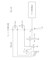
- 積層された第1のダイと第2のダイを含むイベントベースビジョンセンサであって、
前記第1のダイに画素アレイの各画素のフォトダイオードが配置され、
前記第2のダイに画素アレイの各画素のイベント検出器と、光強度に依存するフォトレセプタ信号を生成して前記イベント検出器に入力するフォトレセプタ回路が配置され、
前記フォトレセプタ回路は、複数のトランジスタで構成され、
前記イベント検出器は、メモリキャパシタと、比較器と、メモリとを有し、
前記メモリキャパシタは、MIM(金属-絶縁体-金属構造)キャパシタで構成され、前記MIMキャパシタの第1のプレートは前記フォトレセプタ回路により生成されたフォトレセプタ信号と接続され、前記MIMキャパシタの第2のプレートは前記比較器の一方の入力に接続され、前記比較器の他方の入力はコントローラによって適用される閾値信号と接続され、
前記比較器の出力は前記メモリに記憶されるように構成される、
イベントベースビジョンセンサ。 - 請求項1に記載のイベントベースビジョンセンサであって、
前記MIMキャパシタの前記第2のプレートと前記比較器の一方の入力との間には条件付きリセット回路が接続され、前記条件付きリセット回路は、前記メモリに記憶された前記比較器の出力とコントローラによって適用されるリセット信号との組み合わせに基づいて導通状態が切り替えられるように構成される、
イベントベースビジョンセンサ。 - 請求項1に記載のイベントベースビジョンセンサであって、
前記第1のダイは配線層が光入射面とは反対側に配置される裏面照射構造を有する
イベントベースビジョンセンサ。 - 請求項1に記載のイベントベースビジョンセンサであって、
前記第1のダイと前記第2のダイはCu-Cu接合部を用いて互いに接続される
イベントベースビジョンセンサ。 - 請求項1に記載のイベントベースビジョンセンサであって、
前記第1のダイ及び/又は前記第2のダイは積層ダイを含み、前記積層ダイは、スルーシリコンビア接続を有する
イベントベースビジョンセンサ。 - 請求項1に記載のイベントベースビジョンセンサであって、
前記フォトレセプタ回路は、n-FETトランジスタ及びp-FETトランジスタを含む
イベントベースビジョンセンサ。 - 請求項1に記載のイベントベースビジョンセンサであって、
前記フォトレセプタ回路は、2つのn-FETトランジスタとp-FETトランジスタを含む
イベントベースビジョンセンサ。
Applications Claiming Priority (4)
| Application Number | Priority Date | Filing Date | Title |
|---|---|---|---|
| US201862642838P | 2018-03-14 | 2018-03-14 | |
| US62/642,838 | 2018-03-14 | ||
| PCT/IB2019/051920 WO2019175733A1 (en) | 2018-03-14 | 2019-03-08 | Event-based vision sensor manufactured with 3d-ic technology |
| JP2020571913A JP2021516872A (ja) | 2018-03-14 | 2019-03-08 | 3d−ic技術を用いて製造するイベントベースビジョンセンサ |
Related Parent Applications (1)
| Application Number | Title | Priority Date | Filing Date |
|---|---|---|---|
| JP2020571913A Division JP2021516872A (ja) | 2018-03-14 | 2019-03-08 | 3d−ic技術を用いて製造するイベントベースビジョンセンサ |
Publications (2)
| Publication Number | Publication Date |
|---|---|
| JP2023164990A JP2023164990A (ja) | 2023-11-14 |
| JP7630575B2 true JP7630575B2 (ja) | 2025-02-17 |
Family
ID=66102157
Family Applications (2)
| Application Number | Title | Priority Date | Filing Date |
|---|---|---|---|
| JP2020571913A Pending JP2021516872A (ja) | 2018-03-14 | 2019-03-08 | 3d−ic技術を用いて製造するイベントベースビジョンセンサ |
| JP2023145998A Active JP7630575B2 (ja) | 2018-03-14 | 2023-09-08 | 3d-ic技術を用いて製造するイベントベースビジョンセンサ |
Family Applications Before (1)
| Application Number | Title | Priority Date | Filing Date |
|---|---|---|---|
| JP2020571913A Pending JP2021516872A (ja) | 2018-03-14 | 2019-03-08 | 3d−ic技術を用いて製造するイベントベースビジョンセンサ |
Country Status (6)
| Country | Link |
|---|---|
| US (2) | US10923520B2 (ja) |
| EP (1) | EP3766099A1 (ja) |
| JP (2) | JP2021516872A (ja) |
| KR (1) | KR20210028139A (ja) |
| CN (2) | CN119946453A (ja) |
| WO (1) | WO2019175733A1 (ja) |
Families Citing this family (8)
| Publication number | Priority date | Publication date | Assignee | Title |
|---|---|---|---|---|
| WO2020027230A1 (ja) * | 2018-07-31 | 2020-02-06 | ソニーセミコンダクタソリューションズ株式会社 | 積層型受光センサ及び車載撮像装置 |
| WO2020100663A1 (ja) * | 2018-11-16 | 2020-05-22 | ソニーセミコンダクタソリューションズ株式会社 | 固体撮像装置及び撮像装置 |
| KR20230026999A (ko) * | 2020-06-19 | 2023-02-27 | 소니 세미컨덕터 솔루션즈 가부시키가이샤 | 촬상 장치 |
| EP3962069B1 (en) * | 2020-08-31 | 2024-10-16 | IniVation AG | Event sensor and method for generating a signal stream comprising event data |
| WO2022065033A1 (ja) * | 2020-09-28 | 2022-03-31 | ソニーセミコンダクタソリューションズ株式会社 | 電子機器及び電子機器の制御方法 |
| JP2022108423A (ja) * | 2021-01-13 | 2022-07-26 | ソニーセミコンダクタソリューションズ株式会社 | 固体撮像素子、撮像装置 |
| US12470849B2 (en) * | 2022-12-15 | 2025-11-11 | Prophesee | Event sensor pixel with sensitivity and dynamic range optimization |
| WO2025057566A1 (ja) * | 2023-09-13 | 2025-03-20 | ソニーセミコンダクタソリューションズ株式会社 | 固体撮像素子、電子機器、および、固体撮像素子の制御方法 |
Citations (29)
| Publication number | Priority date | Publication date | Assignee | Title |
|---|---|---|---|---|
| US5887049A (en) | 1996-11-12 | 1999-03-23 | California Institute Of Technology | Self-triggered X-ray sensor |
| JP2002507864A (ja) | 1998-03-16 | 2002-03-12 | フォトン ビジョン システムズ、エルエルシー | Cmosイメージング装置 |
| JP2002209838A (ja) | 2001-01-22 | 2002-07-30 | Olympus Optical Co Ltd | 内視鏡撮像装置 |
| JP2004350153A (ja) | 2003-05-23 | 2004-12-09 | Minolta Co Ltd | 撮像装置 |
| JP2006191081A (ja) | 2004-12-30 | 2006-07-20 | Magnachip Semiconductor Ltd | 受光領域が拡張されたイメージセンサ及びその製造方法 |
| JP2008544571A (ja) | 2005-06-28 | 2008-12-04 | シリコンファイル・テクノロジーズ・インコーポレイテッド | 3次元構造を持つイメージセンサの分離型単位画素及びその製造方法 |
| JP2009508085A (ja) | 2005-06-03 | 2009-02-26 | ウニヴェルズィテート チューリッヒ | 時間依存性の画像データを検出するフォトアレイ |
| WO2011077580A1 (ja) | 2009-12-26 | 2011-06-30 | キヤノン株式会社 | 固体撮像装置および撮像システム |
| US20120261553A1 (en) | 2011-04-13 | 2012-10-18 | Semi Conductor Devices-Elbit Systems-Rafael Partnership | Detector pixel signal readout circuit and an imaging method thereof |
| US20120267511A1 (en) | 2011-04-19 | 2012-10-25 | Altasens, Inc. | Image sensor with hybrid heterostructure |
| JP2013009294A (ja) | 2011-05-25 | 2013-01-10 | Olympus Corp | 固体撮像装置、撮像装置、および信号読み出し方法 |
| JP2013051674A (ja) | 2011-08-02 | 2013-03-14 | Canon Inc | 周辺回路を配置しチップ面積増大を抑制した撮像素子及び撮像装置 |
| US20130075593A1 (en) | 2004-11-19 | 2013-03-28 | Voxtel, Inc. | Active pixel sensors with variable threshold reset |
| JP2013530511A (ja) | 2010-06-02 | 2013-07-25 | ソニー株式会社 | 固体撮像装置、固体撮像装置の製造方法、および電子機器 |
| JP2014090394A (ja) | 2012-10-29 | 2014-05-15 | Koichi Sekine | 動き検出用固体撮像装置および動き検出システム |
| JP2015065524A (ja) | 2013-09-24 | 2015-04-09 | 株式会社ニコン | 撮像素子および撮像装置 |
| US20150194454A1 (en) | 2014-01-08 | 2015-07-09 | Moo Young Kim | Vision sensor chip with open-loop amplifier, operating method, and data processing system including same |
| JP2015530855A (ja) | 2012-10-05 | 2015-10-15 | ラムバス・インコーポレーテッド | 条件付きリセットのマルチビット読み出しイメージセンサ |
| US20150365617A1 (en) | 2013-01-31 | 2015-12-17 | Nanyang Technological University | Image sensors and methods for controlling an image sensor |
| JP2016092661A (ja) | 2014-11-07 | 2016-05-23 | ソニー株式会社 | 撮像素子および駆動方法、並びに電子機器 |
| US20160191829A1 (en) | 2014-12-24 | 2016-06-30 | General Electric Company | Systems and methods for mimimizing silicon photomultiplier signal propagation delay dispersion and improve timing |
| JP2016139936A (ja) | 2015-01-27 | 2016-08-04 | 株式会社東芝 | 固体撮像装置 |
| US20160358967A1 (en) | 2015-06-03 | 2016-12-08 | Semiconductor Components Industries, Llc | Monolithically stacked image sensors |
| WO2017009944A1 (ja) | 2015-07-14 | 2017-01-19 | オリンパス株式会社 | 固体撮像装置 |
| WO2017013806A1 (ja) | 2015-07-23 | 2017-01-26 | オリンパス株式会社 | 固体撮像装置 |
| WO2017018215A1 (ja) | 2015-07-27 | 2017-02-02 | ソニー株式会社 | 固体撮像装置およびその制御方法、並びに電子機器 |
| JP2017059937A (ja) | 2015-09-15 | 2017-03-23 | 株式会社Jvcケンウッド | 固体撮像装置 |
| WO2017169480A1 (ja) | 2016-03-31 | 2017-10-05 | 株式会社ニコン | 撮像素子および撮像装置 |
| US20170350990A1 (en) | 2015-02-23 | 2017-12-07 | Institut de Física D'Altes Energies | Photon counting |
Family Cites Families (9)
| Publication number | Priority date | Publication date | Assignee | Title |
|---|---|---|---|---|
| EP0871902B1 (en) * | 1994-12-23 | 2005-06-15 | Digirad Corporation | Semiconductor gamma-ray camera and medical imaging system |
| KR101887988B1 (ko) * | 2012-07-03 | 2018-08-14 | 삼성전자 주식회사 | 이미지 센서 칩, 이의 동작 방법, 및 이를 포함하는 시스템 |
| KR20140056986A (ko) * | 2012-11-02 | 2014-05-12 | 삼성전자주식회사 | 모션 센서 어레이 장치, 상기 모선 센서 어레이를 이용한 거리 센싱 시스템, 및 거리 센싱 방법 |
| US20170337469A1 (en) * | 2016-05-17 | 2017-11-23 | Agt International Gmbh | Anomaly detection using spiking neural networks |
| JP6651079B2 (ja) | 2016-05-25 | 2020-02-19 | 株式会社ササキコーポレーション | 球根植付け機の球根装填部 |
| JP2017209045A (ja) | 2016-05-25 | 2017-11-30 | 日油株式会社 | 乳飲料 |
| WO2018122798A1 (en) | 2016-12-30 | 2018-07-05 | Insightness Ag | Dynamic vision sensor architecture |
| WO2019087472A1 (ja) * | 2017-10-30 | 2019-05-09 | ソニーセミコンダクタソリューションズ株式会社 | 固体撮像素子 |
| US11082656B2 (en) * | 2017-10-30 | 2021-08-03 | Sony Semiconductor Solutions Corporation | Solid-state imaging device |
-
2019
- 2019-03-08 CN CN202510102693.3A patent/CN119946453A/zh active Pending
- 2019-03-08 EP EP19716563.2A patent/EP3766099A1/en active Pending
- 2019-03-08 US US16/297,267 patent/US10923520B2/en active Active
- 2019-03-08 CN CN201980018550.7A patent/CN112243536B/zh active Active
- 2019-03-08 JP JP2020571913A patent/JP2021516872A/ja active Pending
- 2019-03-08 WO PCT/IB2019/051920 patent/WO2019175733A1/en not_active Ceased
- 2019-03-08 KR KR1020207026285A patent/KR20210028139A/ko not_active Ceased
-
2021
- 2021-01-29 US US17/161,961 patent/US11652126B2/en active Active
-
2023
- 2023-09-08 JP JP2023145998A patent/JP7630575B2/ja active Active
Patent Citations (29)
| Publication number | Priority date | Publication date | Assignee | Title |
|---|---|---|---|---|
| US5887049A (en) | 1996-11-12 | 1999-03-23 | California Institute Of Technology | Self-triggered X-ray sensor |
| JP2002507864A (ja) | 1998-03-16 | 2002-03-12 | フォトン ビジョン システムズ、エルエルシー | Cmosイメージング装置 |
| JP2002209838A (ja) | 2001-01-22 | 2002-07-30 | Olympus Optical Co Ltd | 内視鏡撮像装置 |
| JP2004350153A (ja) | 2003-05-23 | 2004-12-09 | Minolta Co Ltd | 撮像装置 |
| US20130075593A1 (en) | 2004-11-19 | 2013-03-28 | Voxtel, Inc. | Active pixel sensors with variable threshold reset |
| JP2006191081A (ja) | 2004-12-30 | 2006-07-20 | Magnachip Semiconductor Ltd | 受光領域が拡張されたイメージセンサ及びその製造方法 |
| JP2009508085A (ja) | 2005-06-03 | 2009-02-26 | ウニヴェルズィテート チューリッヒ | 時間依存性の画像データを検出するフォトアレイ |
| JP2008544571A (ja) | 2005-06-28 | 2008-12-04 | シリコンファイル・テクノロジーズ・インコーポレイテッド | 3次元構造を持つイメージセンサの分離型単位画素及びその製造方法 |
| WO2011077580A1 (ja) | 2009-12-26 | 2011-06-30 | キヤノン株式会社 | 固体撮像装置および撮像システム |
| JP2013530511A (ja) | 2010-06-02 | 2013-07-25 | ソニー株式会社 | 固体撮像装置、固体撮像装置の製造方法、および電子機器 |
| US20120261553A1 (en) | 2011-04-13 | 2012-10-18 | Semi Conductor Devices-Elbit Systems-Rafael Partnership | Detector pixel signal readout circuit and an imaging method thereof |
| US20120267511A1 (en) | 2011-04-19 | 2012-10-25 | Altasens, Inc. | Image sensor with hybrid heterostructure |
| JP2013009294A (ja) | 2011-05-25 | 2013-01-10 | Olympus Corp | 固体撮像装置、撮像装置、および信号読み出し方法 |
| JP2013051674A (ja) | 2011-08-02 | 2013-03-14 | Canon Inc | 周辺回路を配置しチップ面積増大を抑制した撮像素子及び撮像装置 |
| JP2015530855A (ja) | 2012-10-05 | 2015-10-15 | ラムバス・インコーポレーテッド | 条件付きリセットのマルチビット読み出しイメージセンサ |
| JP2014090394A (ja) | 2012-10-29 | 2014-05-15 | Koichi Sekine | 動き検出用固体撮像装置および動き検出システム |
| US20150365617A1 (en) | 2013-01-31 | 2015-12-17 | Nanyang Technological University | Image sensors and methods for controlling an image sensor |
| JP2015065524A (ja) | 2013-09-24 | 2015-04-09 | 株式会社ニコン | 撮像素子および撮像装置 |
| US20150194454A1 (en) | 2014-01-08 | 2015-07-09 | Moo Young Kim | Vision sensor chip with open-loop amplifier, operating method, and data processing system including same |
| JP2016092661A (ja) | 2014-11-07 | 2016-05-23 | ソニー株式会社 | 撮像素子および駆動方法、並びに電子機器 |
| US20160191829A1 (en) | 2014-12-24 | 2016-06-30 | General Electric Company | Systems and methods for mimimizing silicon photomultiplier signal propagation delay dispersion and improve timing |
| JP2016139936A (ja) | 2015-01-27 | 2016-08-04 | 株式会社東芝 | 固体撮像装置 |
| US20170350990A1 (en) | 2015-02-23 | 2017-12-07 | Institut de Física D'Altes Energies | Photon counting |
| US20160358967A1 (en) | 2015-06-03 | 2016-12-08 | Semiconductor Components Industries, Llc | Monolithically stacked image sensors |
| WO2017009944A1 (ja) | 2015-07-14 | 2017-01-19 | オリンパス株式会社 | 固体撮像装置 |
| WO2017013806A1 (ja) | 2015-07-23 | 2017-01-26 | オリンパス株式会社 | 固体撮像装置 |
| WO2017018215A1 (ja) | 2015-07-27 | 2017-02-02 | ソニー株式会社 | 固体撮像装置およびその制御方法、並びに電子機器 |
| JP2017059937A (ja) | 2015-09-15 | 2017-03-23 | 株式会社Jvcケンウッド | 固体撮像装置 |
| WO2017169480A1 (ja) | 2016-03-31 | 2017-10-05 | 株式会社ニコン | 撮像素子および撮像装置 |
Also Published As
| Publication number | Publication date |
|---|---|
| CN112243536A (zh) | 2021-01-19 |
| CN112243536B (zh) | 2025-03-07 |
| US10923520B2 (en) | 2021-02-16 |
| US20190288024A1 (en) | 2019-09-19 |
| US20210151492A1 (en) | 2021-05-20 |
| EP3766099A1 (en) | 2021-01-20 |
| KR20210028139A (ko) | 2021-03-11 |
| CN119946453A (zh) | 2025-05-06 |
| JP2021516872A (ja) | 2021-07-08 |
| WO2019175733A1 (en) | 2019-09-19 |
| KR20230170980A (ko) | 2023-12-19 |
| JP2023164990A (ja) | 2023-11-14 |
| US11652126B2 (en) | 2023-05-16 |
Similar Documents
| Publication | Publication Date | Title |
|---|---|---|
| JP7630575B2 (ja) | 3d-ic技術を用いて製造するイベントベースビジョンセンサ | |
| TWI701824B (zh) | 影像感測器、積體電路及形成影像感測器的方法 | |
| US8957358B2 (en) | CMOS image sensor chips with stacked scheme and methods for forming the same | |
| US10312275B2 (en) | Single-photon avalanche diode image sensor with photon counting and time-of-flight detection capabilities | |
| US9153565B2 (en) | Image sensors with a high fill-factor | |
| US7710477B2 (en) | CMOS image sensors having pixel arrays with uniform light sensitivity | |
| KR101514119B1 (ko) | 적층된 방식의 cmos 이미지 센서 칩들 및 그 형성 방법 | |
| EP2426718B1 (en) | Semiconductor device, manufacturing method therefor, and electronic apparatus | |
| US8089543B2 (en) | Solid-state image pickup element and solid-state image pickup device | |
| US10070079B2 (en) | High dynamic range global shutter image sensors having high shutter efficiency | |
| KR20180136874A (ko) | 고체 촬상 소자 및 그 제조 방법 | |
| JP2020047734A (ja) | 固体撮像装置及び電子機器 | |
| WO2020137334A1 (ja) | 光電変換素子、固体撮像装置及び電子機器 | |
| US20250351609A1 (en) | Stacked image sensors and methods of manufacturing thereof | |
| JP7532025B2 (ja) | 半導体装置および機器 | |
| CN107425026A (zh) | 半导体器件及其制造方法 | |
| CN118743024A (zh) | 光检测装置和电子设备 | |
| JP2008135780A (ja) | X−yアドレス型固体撮像素子の製造方法 | |
| CN220963352U (zh) | 集成芯片以及半导体结构 | |
| TWI913534B (zh) | 積體晶片及其形成方法以及半導體結構 | |
| US12237355B2 (en) | Semiconductor device and semiconductor die | |
| Wang et al. | Readout Circuits for Three-dimensional Integration of Single-photon Avalanche Diode Detector Arrays | |
| CN120898546A (zh) | 光检测装置和电子设备 | |
| JP2017188615A (ja) | 固体撮像装置 | |
| JP2012129552A (ja) | 固体撮像素子 |
Legal Events
| Date | Code | Title | Description |
|---|---|---|---|
| A621 | Written request for application examination |
Free format text: JAPANESE INTERMEDIATE CODE: A621 Effective date: 20230908 |
|
| A977 | Report on retrieval |
Free format text: JAPANESE INTERMEDIATE CODE: A971007 Effective date: 20240705 |
|
| A131 | Notification of reasons for refusal |
Free format text: JAPANESE INTERMEDIATE CODE: A131 Effective date: 20240730 |
|
| A521 | Request for written amendment filed |
Free format text: JAPANESE INTERMEDIATE CODE: A523 Effective date: 20241028 |
|
| TRDD | Decision of grant or rejection written | ||
| A01 | Written decision to grant a patent or to grant a registration (utility model) |
Free format text: JAPANESE INTERMEDIATE CODE: A01 Effective date: 20250107 |
|
| A61 | First payment of annual fees (during grant procedure) |
Free format text: JAPANESE INTERMEDIATE CODE: A61 Effective date: 20250204 |
|
| R150 | Certificate of patent or registration of utility model |
Ref document number: 7630575 Country of ref document: JP Free format text: JAPANESE INTERMEDIATE CODE: R150 |