JP7631994B2 - Particulate filter and method for manufacturing particulate filter - Google Patents
Particulate filter and method for manufacturing particulate filter Download PDFInfo
- Publication number
- JP7631994B2 JP7631994B2 JP2021060626A JP2021060626A JP7631994B2 JP 7631994 B2 JP7631994 B2 JP 7631994B2 JP 2021060626 A JP2021060626 A JP 2021060626A JP 2021060626 A JP2021060626 A JP 2021060626A JP 7631994 B2 JP7631994 B2 JP 7631994B2
- Authority
- JP
- Japan
- Prior art keywords
- substrate
- hole
- coating layer
- particulate filter
- sectional dimension
- Prior art date
- Legal status (The legal status is an assumption and is not a legal conclusion. Google has not performed a legal analysis and makes no representation as to the accuracy of the status listed.)
- Active
Links
Images




Classifications
-
- B—PERFORMING OPERATIONS; TRANSPORTING
- B01—PHYSICAL OR CHEMICAL PROCESSES OR APPARATUS IN GENERAL
- B01D—SEPARATION
- B01D39/00—Filtering material for liquid or gaseous fluids
- B01D39/14—Other self-supporting filtering material ; Other filtering material
- B01D39/16—Other self-supporting filtering material ; Other filtering material of organic material, e.g. synthetic fibres
-
- B—PERFORMING OPERATIONS; TRANSPORTING
- B01—PHYSICAL OR CHEMICAL PROCESSES OR APPARATUS IN GENERAL
- B01D—SEPARATION
- B01D39/00—Filtering material for liquid or gaseous fluids
- B01D39/14—Other self-supporting filtering material ; Other filtering material
- B01D39/20—Other self-supporting filtering material ; Other filtering material of inorganic material, e.g. asbestos paper, metallic filtering material of non-woven wires
-
- B—PERFORMING OPERATIONS; TRANSPORTING
- B23—MACHINE TOOLS; METAL-WORKING NOT OTHERWISE PROVIDED FOR
- B23K—SOLDERING OR UNSOLDERING; WELDING; CLADDING OR PLATING BY SOLDERING OR WELDING; CUTTING BY APPLYING HEAT LOCALLY, e.g. FLAME CUTTING; WORKING BY LASER BEAM
- B23K26/00—Working by laser beam, e.g. welding, cutting or boring
- B23K26/36—Removing material
- B23K26/38—Removing material by boring or cutting
- B23K26/382—Removing material by boring or cutting by boring
-
- C—CHEMISTRY; METALLURGY
- C03—GLASS; MINERAL OR SLAG WOOL
- C03B—MANUFACTURE, SHAPING, OR SUPPLEMENTARY PROCESSES
- C03B33/00—Severing cooled glass
- C03B33/09—Severing cooled glass by thermal shock
Landscapes
- Chemical & Material Sciences (AREA)
- Engineering & Computer Science (AREA)
- Physics & Mathematics (AREA)
- Chemical Kinetics & Catalysis (AREA)
- Optics & Photonics (AREA)
- Organic Chemistry (AREA)
- Materials Engineering (AREA)
- Plasma & Fusion (AREA)
- Mechanical Engineering (AREA)
- Life Sciences & Earth Sciences (AREA)
- Geology (AREA)
- Thermal Sciences (AREA)
- Filtering Materials (AREA)
- Laser Beam Processing (AREA)
- Re-Forming, After-Treatment, Cutting And Transporting Of Glass Products (AREA)
Description
本発明は、微粒子捕捉用フィルタに関する。 The present invention relates to a filter for capturing fine particles.
溶液中に含まれる異物を適切に捕獲することが可能な微粒子捕捉用フィルタは、医療施設、医薬品製造工場、および高清浄度クリーンルームなど、多くの分野でニーズがある。 Particulate filters that can adequately capture foreign matter contained in solutions are in demand in many fields, including medical facilities, pharmaceutical manufacturing plants, and high-purity clean rooms.
微粒子捕捉用フィルタの一構成例として、フィルタの溶液流路の一部に微細な貫通孔を設け、該貫通孔内に微粒子を捕捉させる方式が考えられる。 One possible configuration for a filter for capturing fine particles is to provide minute through-holes in a part of the solution flow path of the filter, and capture the fine particles within the through-holes.
また、そのような微粒子捕捉用フィルタを量産する際に、レーザ加工技術を利用することが考えられる。レーザ加工技術では、被処理体に対して、高い寸法精度で多数の貫通孔を迅速に形成できるためである(例えば、特許文献1)。 In addition, when mass-producing such particulate filters, it is possible to use laser processing technology, because this technology can quickly form a large number of through holes in the workpiece with high dimensional accuracy (for example, Patent Document 1).
ただし、微粒子捕捉用フィルタでは、微粒子を確実に捕捉するため、例えば0.6μm以下程度の、極めて微細な貫通孔(微細貫通孔)を形成する必要がある。しかしながら、一般に、レーザ加工技術では、厚さ50μm以上の被処理体に形成される孔の直径は、2μm程度が限界である。このため、高い精度で前述のような微粒子捕捉用の貫通孔を形成することは容易ではない。 However, in order to reliably capture particles, it is necessary to form extremely fine through-holes (fine through-holes) of, for example, about 0.6 μm or less in size in a particulate capture filter. However, generally, with laser processing technology, the diameter of holes formed in a workpiece having a thickness of 50 μm or more is limited to about 2 μm. For this reason, it is not easy to form the above-mentioned through-holes for capturing particles with high precision.
特に、微粒子捕捉用フィルタでは、例えば、1mm×1mmの検査領域に、1,000個以上の大量の貫通孔を形成する必要が生じ得る。しかしながら、そのような微小な検査領域に対して、レーザ加工法技術により、直径が2μm未満の貫通孔を大量に形成することは極めて難しい。 In particular, in particulate capture filters, it may be necessary to form a large number of through holes, for example 1,000 or more, in an inspection area of 1 mm x 1 mm. However, it is extremely difficult to form a large number of through holes with a diameter of less than 2 μm in such a small inspection area using laser processing technology.
このような背景により、これまで、レーザ加工技術を用いて微粒子捕捉用フィルタを製造した例は、ほとんど認められない。しかしながら、レーザ加工技術を用いて微粒子捕捉用フィルタを製造することができれば、品質や製造コストの点で好ましいと考えられる。 Due to this background, there have been almost no examples to date of using laser processing technology to manufacture particulate filters. However, if it were possible to manufacture particulate filters using laser processing technology, it would be preferable in terms of quality and manufacturing costs.
本発明は、このような背景に鑑みなされたものであり、本発明では、レーザ加工技術を利用して製造することが可能な構成を有する、微粒子捕捉用フィルタを提供することを目的とする。また、本発明では、そのような微粒子捕捉用フィルタの製造方法を提供することを目的とする。 The present invention has been made in consideration of the above background, and aims to provide a particulate filter having a configuration that can be manufactured using laser processing technology. It also aims to provide a method for manufacturing such a particulate filter.
本発明では、微粒子捕捉用フィルタであって、
第1の表面および第2の表面を有し、厚さが50μm以上である透明な本体と、
該本体の前記第1の表面から前記第2の表面まで貫通する複数の貫通孔と、
を有し、
前記第2の表面からの深さが10μmの位置を基準深さDSと定め、
各貫通孔において、前記基準深さDSにおける最小断面寸法)をφPとし、前記基準深さDSと前記第2の表面との間における最小断面寸法をφQとしたとき、
φQ≦0.6μmであり、φQ/φP≦0.5である、微粒子捕捉用フィルタが提供される。
The present invention provides a particulate filter, comprising:
a transparent body having a first surface and a second surface and a thickness of 50 μm or more;
a plurality of through holes extending from the first surface to the second surface of the body;
having
A position at a depth of 10 μm from the second surface is defined as a reference depth D S ;
In each through hole, when the minimum cross-sectional dimension at the reference depth D S is φ P and the minimum cross-sectional dimension between the reference depth D S and the second surface is φ Q ,
A particulate filter is provided in which φ Q ≦0.6 μm and φ Q /φ P ≦0.5.
また、本発明では、微粒子捕捉用フィルタの製造方法であって、
(I)相互に対向する第1の表面および第2の表面を有する透明な基材を準備する工程と、
(II)前記基材の前記第1の表面にレーザ光を照射し、前記基材に前記第1の表面から前記第2の表面まで貫通する、複数の基材貫通孔を形成する工程と、
(III)前記基材の前記第2の表面にコーティング層を設置して、前記基材および前記コーティング層を貫通する複数の貫通孔を形成する工程と、
を有する、製造方法が提供される。
The present invention also provides a method for producing a particulate filter, comprising the steps of:
(I) providing a transparent substrate having a first surface and a second surface opposed to each other;
(II) irradiating the first surface of the substrate with laser light to form a plurality of substrate through-holes penetrating the substrate from the first surface to the second surface;
(III) providing a coating layer on the second surface of the substrate to form a plurality of through holes through the substrate and the coating layer;
A method of manufacturing is provided, comprising:
本発明では、レーザ加工技術を利用して製造することが可能な構成を有する、微粒子捕捉用フィルタを提供することができる。また、本発明では、そのような微粒子捕捉用フィルタの製造方法を提供することを目的とする。 The present invention provides a particulate filter having a configuration that can be manufactured using laser processing technology. It is also an object of the present invention to provide a method for manufacturing such a particulate filter.
以下、本発明の一実施形態について説明する。 One embodiment of the present invention is described below.
本発明の一実施形態では、微粒子捕捉用フィルタであって、
第1の表面および第2の表面を有し、厚さが50μm以上である透明な本体と、
該本体の前記第1の表面から前記第2の表面まで貫通する複数の貫通孔と、
を有し、
前記第2の表面からの深さが10μmの位置を基準深さDSと定め、
各貫通孔において、前記基準深さDSにおける最小断面寸法)をφPとし、前記基準深さDSと前記第2の表面との間における最小断面寸法をφQとしたとき、
φQ≦0.6μmであり、φQ/φP≦0.5である、微粒子捕捉用フィルタが提供される。
In one embodiment of the present invention, there is provided a particulate filter comprising:
a transparent body having a first surface and a second surface and a thickness of 50 μm or more;
a plurality of through holes extending from the first surface to the second surface of the body;
having
A position at a depth of 10 μm from the second surface is defined as a reference depth D S ;
In each through hole, when the minimum cross-sectional dimension at the reference depth D S is φ P and the minimum cross-sectional dimension between the reference depth D S and the second surface is φ Q ,
A particulate filter is provided in which φ Q ≦0.6 μm and φ Q /φ P ≦0.5.
前述のように、レーザ加工技術では、厚さ50μm以上の被処理体に形成される孔の直径は、2μm程度が限界であり、高い精度でより微細な孔を形成することは容易ではない。特に、微小な検査領域に対して、レーザ加工法技術により、直径が2μm未満の貫通孔を大量に形成することは極めて難しい。 As mentioned above, with laser processing technology, the diameter of holes formed in a workpiece having a thickness of 50 μm or more is limited to about 2 μm, and it is not easy to form finer holes with high precision. In particular, it is extremely difficult to mass-form through holes with a diameter of less than 2 μm in a tiny inspection area using laser processing technology.
この点、本発明の一実施形態による微粒子捕捉用フィルタは、上記のような構成を有する。このような構成を有する微粒子捕捉用フィルタは、後に詳しく示すように、50μm以上の厚さを有するものの、レーザ加工技術を利用して製造することができる。 In this regard, the particulate filter according to one embodiment of the present invention has the above-mentioned configuration. As will be described in detail later, a particulate filter having such a configuration has a thickness of 50 μm or more, but can be manufactured using laser processing technology.
従って、本発明の一実施形態では、高品質および低製造コストで、微粒子捕捉用フィルタを製造することができる。 Therefore, in one embodiment of the present invention, a particulate capture filter can be manufactured with high quality and low manufacturing costs.
(本発明の一実施形態による微粒子捕捉用フィルタ)
以下、図面を参照して、本発明の一実施形態について、より詳しく説明する。
(Particulate filter according to one embodiment of the present invention)
Hereinafter, an embodiment of the present invention will be described in more detail with reference to the drawings.
図1および図2には、本発明の一実施形態による微粒子捕捉用フィルタの一構成例を模式的に示す。図1には、本発明の一実施形態による微粒子捕捉用フィルタ(以下、「第1のフィルタ」と称する)の上面図が示されている。 Figures 1 and 2 show a schematic diagram of an example of the configuration of a particulate filter according to one embodiment of the present invention. Figure 1 shows a top view of a particulate filter according to one embodiment of the present invention (hereinafter referred to as the "first filter").
図1に示すように、第1のフィルタ100は、透明な本体110を有する。本体110は、第1の表面112および第2の表面114を有する。本体110には、検査領域120が配置される。
As shown in FIG. 1, the
なお、図1に示した例では、第1のフィルタ100は、上面視、略円形の形態を有する。ただし、第1のフィルタ100の形態は、特に限られず、例えば、楕円形、三角形、四角形、または五角形以上の多角形であってもよい。
In the example shown in FIG. 1, the
また、図1に示した例では、検査領域120は、上面視、本体110の略中央に、略正方形状に配置されている。しかしながら、これは単なる一例に過ぎない。検査領域120は、本体110の非中央部分に配置されてもよい。また、検査領域120は、非正方形状、例えば、円形状、楕円形状、矩形状、または五角形以上の多角形状に配置されてもよい。
In the example shown in FIG. 1, the
また、検査領域120の数は、必ずしも1箇所に限られず、検査領域120は、本体110の複数の箇所に設けられてもよい。
In addition, the number of
さらに、図1では、検査領域120が矩形状の枠により、明確に表されている。しかしながら、第1のフィルタ100において、目視では、検査領域120と非検査領域の境界が明確に識別できない場合も、しばしばあり得ることに留意する必要がある。
Furthermore, in FIG. 1, the
図1の左側の丸枠内には、検査領域120の一部を拡大して示す。この枠内に示すように、検査領域120には、多数の貫通孔122が形成されている。
The circular frame on the left side of FIG. 1 shows an enlarged view of a portion of the
検査領域120における貫通孔122の密度は、特に限られないが、例えば、100個/mm2以上である。
The density of the through
貫通孔122の二次元配列の形態は、特に限られない。貫通孔122は、規則的に配列されても、ランダムに配列されてもよい。
The form of the two-dimensional arrangement of the through
また、貫通孔122が規則的に配列される場合、配列の態様およびピッチなどは、特に限られない。例えば、図1に示したように、貫通孔122は、縦横に規則的に配列されてもよい。ピッチは、例えば、10μm~100μmの範囲であってもよい。
When the through
図2には、本体110の検査領域120の断面の一例を模式的に示す。図2には、複数の貫通孔122の長手中心軸に沿った断面が示されている。
Figure 2 shows a schematic example of a cross section of the
図2に示すように、本体110は、基材140と、該基材140の一方の表面に形成されたコーティング層150とを有する。本体110の第1の表面112は、基材140のコーティング層150が設置されていない側の表面に対応し、第2の表面114は、コーティング層の表面に対応する。
As shown in FIG. 2, the
図2において、破線Diは、基材140とコーティング層150の間の境界を表す。ただし、実際には、この境界Diが不明瞭な場合もしばしば生じ得る。
2, the dashed line D i represents the boundary between the
本体110には、多数の貫通孔122が含まれる。各貫通孔122は、本体110の第1の表面112の側に、第1の開口125を有し、第2の表面114に第2の開口127を有する。
The
各貫通孔122は、基材140およびコーティング層150の両方を貫通することにより、形成されている。従って、貫通孔122の第1の開口125は、基材140側の開口であり、第2の開口127は、コーティング層150側の開口である。
Each through
各貫通孔122において、特に、基材140側の部分を「基材貫通孔132a」と称し、コーティング層150側の部分を「コーティング層貫通孔132b」と称する。
In each through
図2に示した例では、各貫通孔122において、基材貫通孔132aは、テーパー形状を有し、第1の開口125から境界Diまで、「最小断面寸法」が単調に減少する。
In the example shown in FIG. 2, in each through
ここで、「(貫通孔の)最小断面寸法」とは、貫通孔122の長手中心軸を通る断面において、対向する側壁同士の最も小さい距離を意味する。従って、貫通孔の断面が円形の場合、「最小断面寸法」は、直径を表し、楕円の場合、「最小断面寸法」は、短軸の寸法を表す。
Here, the "minimum cross-sectional dimension (of the through hole)" refers to the smallest distance between opposing side walls in a cross section passing through the central longitudinal axis of the through
また、正確には、第1の開口125および第2の開口127は、「貫通孔の断面」ではない。しかしながら、本願では、これらの開口125、127の寸法を表す際にも、「最小断面寸法」と言う用語を使用する。
To be precise, the
図2に示した例では、基材貫通孔132aのテーパー角度θは、例えば、65゜~89゜の範囲である。ここで、基材貫通孔132aのテーパー角度θは、第1の表面112の法線と、基材貫通孔132aの側壁とのなす角で表される。
In the example shown in FIG. 2, the taper angle θ of the substrate through
再度図2を参照すると、貫通孔122のコーティング層貫通孔132bは、基材貫通孔132aに比べて、より複雑な断面形状を有する。
Referring again to FIG. 2, the coating layer through-
例えば、図2に示した例では、コーティング層貫通孔132bは、境界Diから第2の表面114の間(ただし、境界Diは含まない)に、最小断面寸法が最小となる狭窄部154を有する断面形状を有する。すなわち、狭窄部154の最小断面寸法をφQとした場合、φQは、貫通孔122の間で最も小さな最小断面寸法を示す。
2, the coating layer through
ここで、各貫通孔122において、本体110の第2の表面114から深さ10μmの位置を「基準深さ」と称し、DSで表す。図2に示すように、基準深さDSは、境界Diよりも本体110の第2の表面114から遠い位置にある。また、基準深さDSでの貫通孔122の最小断面寸法をφPで表す。
Here, in each through
第1のフィルタ100では、上記のように規定される最小断面寸法φPおよびφQを用いた場合、各貫通孔122が
φQ≦0.6μm、および
φQ/φP≦0.5
を満たすという特徴を有する。
In the
It has the characteristic of satisfying the following.
特に、φQ/φP≦0.4であってもよい。 In particular, φ Q /φ P ≦0.4 may be satisfied.
第1のフィルタ100は、一般的なレーザ加工方法では形成することが難しかった、最小断面寸法φQ≦0.6μmを満たす狭窄部154を、各貫通孔122の内部(または第2の表面114)に有する。
The
従って、第1のフィルタ100は、例えば、粒径が0.6μm超程度の微細な微粒子を捕捉するフィルタとして、利用することができる。
Therefore, the
また、第1のフィルタ100において、基材貫通孔132aの部分は、一般的なレーザ加工技術を用いて形成することができる。レーザ加工技術では、同等の形状の基材貫通孔132aを高精度に形成できる。このため、第1のフィルタ100は、高品質かつ低コストで製造することができる。
In addition, in the
さらに、第1のフィルタ100では、各貫通孔122において、狭窄部154の深さ位置を、第2の表面114から境界Di(ただし、境界Diの位置は除く)までのいずれかの箇所に揃えることができる。この場合、いずれの貫通孔122においても、ほぼ同等の深さ位置で微粒子を捕捉することが可能となり、微粒子の検出が容易となる。
Furthermore, in the
(本発明の一実施形態による微粒子捕捉用フィルタの各部分)
次に、本発明の一実施形態による微粒子捕捉用フィルタの各部分について、より詳しく説明する。
Parts of a Particulate Filter According to an Embodiment of the Invention
Next, each part of the particulate filter according to one embodiment of the present invention will be described in more detail.
なお、ここでは、明確化のため、本発明の一実施形態による微粒子捕捉用フィルタとして、前述の第1のフィルタ100を例に、その各部分について説明する。従って、各部分を表す際には、図1および図2に示した参照符号を使用する。
For clarity, each part of the particulate filter according to one embodiment of the present invention will be described using the
(本体110)
図1に示した例では、本体110は、上面視、略円形の形態を有する。ただし、本体110)の形態は、特に限られず、例えば、楕円形、三角形、四角形、または五角形以上の多角形であってもよい。
(Main body 110)
1, the
本体110は、透明な材料で構成される。ここで、「透明」とは、波長360nm~830nmにおける平均透過率が80%以上であることを意味する。
The
従って、第1のフィルタ100を用いた場合、赤外線分光分析法、ラマン分光分析法、光学顕微鏡、および蛍光顕微鏡など、一般的な光学的手法により、微粒子を検出することができる。
Therefore, when the
本体110の厚さは、50μm以上であり、60μm以上であることが好ましい。なお、本体110には、特に厚さの上限はないが、本体110の厚さは、例えば、1mm以下であってもよい。
The thickness of the
本体110の第1の開口125の最小断面寸法をφ1としたとき、φ1は、5μm≦φ1≦50μmであることが好ましい。
When the minimum cross-sectional dimension of the
また、本体110の第2の開口127の最小断面寸法をφ2としたとき、φ1は、0.2μm≦φ2≦5μmであることが好ましい。
Furthermore, when the minimum cross-sectional dimension of
また、狭窄部154の最小断面寸法φQは、0.2μm以上であることが好ましい。
Furthermore, the minimum cross-sectional dimension φ Q of the narrowed
なお、前述のように、レーザ加工技術のみでは、最小断面寸法が0.6μm以下の貫通孔を形成することは難しい。 As mentioned above, it is difficult to form through holes with a minimum cross-sectional dimension of 0.6 μm or less using laser processing technology alone.
しかしながら、本体110は、基材140およびコーティング層150を有する。従って、第1のフィルタ100では、本体110に、最小断面寸法φQが0.6μm以下の狭窄部154を有する貫通孔122を形成できる。
However, the
狭窄部154の第2の表面114からの深さをdとしたとき、狭窄部154は、0≦d<5μmの範囲に存在してもよい。なお、狭窄部154は、第2の表面114にあってもよいが、境界Diとは異なる位置に存在する。
When the depth of the narrowed
本体110の検査領域120には、100個/mm2以上の密度で貫通孔122が形成されていることが好ましい。貫通孔122の密度は、500個/mm2~15,000個/mm2の範囲であることがより好ましい。
The through
(基材140)
本体110の一部を構成する基材140の種類は、特に限られない。基材140は、例えば、ガラスまたは樹脂のような透明材料で構成されてもよい。
(Substrate 140)
There is no particular limitation on the type of the
基材140の厚さは、50μm以上であることが好ましい。また、基材140の厚さは、例えば、1mm以下であってもよい。
The thickness of the
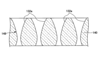
なお、図2に示した基材貫通孔132aの断面形状は、単なる一例であり、基材貫通孔132aは、異なる断面を有してもよい。例えば、基材貫通孔132aは、図3に示すような断面形状を有してもよい。
Note that the cross-sectional shape of the substrate through
図3には、基材貫通孔132aの別の断面を模式的に示す。なお、図3には、本体110のうち、基材140の部分のみが示されており、コーティング層150は示されていない。
Figure 3 shows another cross section of the substrate through
図3に示すように、この基材貫通孔132aは、基材140の内部に基材狭窄部148を有する。基材貫通孔132aは、この基材狭窄部148から、基材140のそれぞれの表面に向かって、「最小断面寸法」が増加するような形状を有する。
As shown in FIG. 3, the substrate through
このような断面形態を有する基材貫通孔132aは、後述するように、微細な貫通孔を有する基材140を湿式エッチング処理した際に、生じ易い。
Substrate through-
このように、本発明の一実施形態において、基材貫通孔132aの断面形状は、特に限られないことに留意する必要がある。
As such, it should be noted that in one embodiment of the present invention, the cross-sectional shape of the substrate through
(コーティング層150)
コーティング層150の種類は、透明である限り、特に限られない。
(Coating layer 150)
The type of
コーティング層150の材料としては、透明であれば特に問われないが、シリカ、アルミナ、酸化マグネシウム、フッ化マグネシウムを主とする材料が低屈折率であり透過率を高く保てる点で好ましい。またシリカ、酸化ハフニウム、酸化タンタル、フッ化マグネシウムを主とする材料が紫外域での消衰係数が小さい点で好ましい。
The material of the
コーティング層150は、特に、シリカまたはフッ化マグネシウムで構成されることが、屈折率が低く、消衰係数が広い波長域で低い点で好ましい。
It is particularly preferable that the
コーティング層150の厚さは、特に限られないが、例えば、0.1μm~5μmの範囲であることが好ましい。
The thickness of the
なお、コーティング層の厚さは、最大10μm以下である。従って、本体110の第2の表面114から境界Diまでの深さは、第2の表面114から基準深さDSまでの距離よりと等しいか、あるいはより小さい。
The thickness of the coating layer is 10 μm or less at most. Therefore, the depth from the
以上、第1のフィルタ100を例に、本発明の一実施形態について説明した。
The above describes one embodiment of the present invention using the
しかしながら、上記記載は、単なる一例であり、本発明の一実施形態による微粒子捕捉用フィルタは、他の形態を有してもよい。 However, the above description is merely an example, and the particulate capture filter according to one embodiment of the present invention may have other configurations.
例えば、図2に示した例では、第1のフィルタ100のコーティング層貫通孔132bは、狭窄部154から第2の表面114に向かって、最小断面寸法が徐々に増加する。しかしながら、これとは異なり、コーティング層貫通孔132bは、境界Diから第2の表面114に向かって、最小断面寸法が徐々に減少する形態を有してもよい。その場合、第2の開口127の最小断面寸法がφQとなる。
2, the coating layer through
また、例えば、コーティング層貫通孔132bは、その一部に、コーティング層の厚さ方向と平行に延在するストレート部分を有してもよい。
For example, the coating layer through
すなわち、本発明の一実施形態による微粒子捕捉用フィルタにおいて、基材貫通孔132aおよびコーティング層貫通孔132bは、前述の特徴を有する限り、いかなる形状を有してもよい。
That is, in a particulate filter according to one embodiment of the present invention, the substrate through-
さらに、上記記載では、透明な本体に貫通孔が形成されている場合を例に、本発明の一実施形態による微粒子捕捉用フィルタについて説明した。しかしながら、本発明の一実施形態による微粒子捕捉用フィルタは、貫通孔の代わりにスリットを有してもよい。 Furthermore, in the above description, a particulate filter according to one embodiment of the present invention has been described using an example in which through-holes are formed in a transparent body. However, a particulate filter according to one embodiment of the present invention may have slits instead of through-holes.
(本発明の一実施形態による微粒子捕捉用フィルタの製造方法)
次に、図4~図8を参照して、本発明の一実施形態による微粒子捕捉用フィルタの製造方法の例について説明する。
(Method of manufacturing a particulate filter according to one embodiment of the present invention)
Next, an example of a method for manufacturing the particulate filter according to one embodiment of the present invention will be described with reference to FIGS.
図4には、本発明の一実施形態による微粒子捕捉用フィルタの製造方法(以下、「第1の方法」と称する)のフローを模式的に示す。 Figure 4 shows a schematic flow diagram of a method for manufacturing a particulate filter according to one embodiment of the present invention (hereinafter referred to as the "first method").
図4に示すように、第1の方法は、
(1)相互に対向する第1の表面および第2の表面を有する透明な基材を準備する工程(工程S110)と、
(2)前記基材の前記第1の表面にレーザ光を照射し、前記基材に前記第1の表面から前記第2の表面まで貫通する、複数の基材貫通孔を形成する工程(工程S120)と、
(3)前記基材の前記第2の表面にコーティング層を設置して、前記基材および前記コーティング層を貫通する複数の貫通孔を形成する工程(工程S130)と、
を有する。
As shown in FIG. 4, the first method is as follows:
(1) preparing a transparent substrate having a first surface and a second surface opposed to each other (step S110);
(2) Irradiating the first surface of the substrate with laser light to form a plurality of substrate through holes penetrating the substrate from the first surface to the second surface (step S120);
(3) providing a coating layer on the second surface of the substrate to form a plurality of through holes penetrating the substrate and the coating layer (step S130);
has.
以下、図5~図8も参照して、各工程について説明する。なお、ここでは、微粒子捕捉用フィルタとして、前述の図1および図2に示した第1のフィルタを例に、その製造方法について説明する。従って、微粒子捕捉用フィルタの各部分を参照する際には、図1および図2に示した参照符号を使用する。 Each step will be described below with reference to Figures 5 to 8. Note that the manufacturing method will be described using the first filter shown in Figures 1 and 2 as an example of a particulate capture filter. Therefore, when referring to each part of the particulate capture filter, the reference symbols shown in Figures 1 and 2 will be used.
(工程S110)
まず、透明な基材140が準備される。
(Step S110)
First, a
図5には、基材140の斜視図を示す。基材140は、第1の表面142および第2の表面144を有する。
Figure 5 shows a perspective view of
なお、図5に示した例では、第1の表面142および第2の表面144は、略円形の形状を有する。しかしながら、第1の表面142および第2の表面144の形状は、特に限られない。第1の表面142および第2の表面144は、例えば、楕円形、三角形、矩形、または五角形以上の多角形等の形状を有してもよい。
In the example shown in FIG. 5, the
基材140は、透明である限り、いかなる材料で構成されてもよい。基材140は、例えば、ガラスまたは樹脂で構成されてもよい。
The
基材140の厚さは、50μm以上であることが好ましい。
The thickness of the
なお、次の工程S120の前に、基材140の第1の表面142に、吸収材が設置されてもよい。吸収材を設置した場合、基材140に照射されるレーザ光のエネルギーをより効率的に吸収することができる。従って、次の工程S120において、より低いエネルギーで高品質にレーザ加工を実施することが可能となる。
In addition, an absorbent material may be placed on the
ただし、吸収材220の設置は任意である。
However, the installation of the
図6には、基材140の第1の表面142に吸収材220が設置された状態を模式的に示す。
Figure 6 shows a schematic diagram of an
吸収層220は、利用されるパルスレーザの少なくとも一部のエネルギーを吸収する機能を有する限り、その材料は特に限られない。吸収層110は、例えば合成樹脂インクやカーボンブラック等を含む顔料であってもよい。
The material of the
(工程S120)
次に、基材140の第1の表面142の側からレーザ光が照射され、基材貫通孔132aが形成される。
(Step S120)
Next, a laser beam is irradiated from the side of the
レーザ光の種類は、特に限られないが、UVレーザが好ましい。 The type of laser light is not particularly limited, but a UV laser is preferred.
レーザ光は、例えば、短パルスレーザであってもよい。 The laser light may be, for example, a short pulse laser.
図7には、基材貫通孔132aが形成された基材140の断面を模式的に示す。なお、図7において、吸収材220は省略されている。
Figure 7 shows a schematic cross section of a
レーザ光の照射により、基材140には、第1の表面142から第2の表面144まで延在する、複数の基材貫通孔132aが形成される。
By irradiating the laser light, a plurality of substrate through-
図7に示すように、レーザ光照射により形成された基材貫通孔132aは、断面が第1の表面142から第2の表面144に向かってテーパー化された形状を有する傾向がある。
As shown in FIG. 7, the substrate through-
テーパー角度θ1は、例えば、65゜~89゜の範囲である。 The taper angle θ 1 is, for example, in the range of 65° to 89°.
各基材貫通孔132aは、基材140の第1の表面142に第1の開口226aを有し、第2の表面144に第2の開口226bを有する。
Each substrate through
第1の開口226aの最小断面寸法は、例えば、4μm~30μmの範囲であり、4μm~15μmの範囲であることが好ましい。
The minimum cross-sectional dimension of the
また、第2の開口226bの最小断面寸法は、例えば、2μm~10μmの範囲であり、2μm~5μmの範囲であることが好ましい。
The minimum cross-sectional dimension of the
形成される基材貫通孔132aの数は、特に限られない。微粒子捕捉用フィルタに利用される場合、基材貫通孔132aの密度は、例えば、100個/mm2以上であり、500個/mm2~15,000個/mm2の範囲であることが好ましい。
The number of the base material through
基材貫通孔132aの形成後に、基材140を湿式エッチング処理してもよい。
After the substrate through-
湿式エッチングを行うことにより、吸収材220およびレーザ加工の際に生じたデブリ等を除去できる。
By performing wet etching, the
例えば、基材140がガラスの場合、湿式エッチング処理は、フッ酸溶液中で実施されてもよい。
For example, if the
なお、湿式エッチング処理を実施した場合、しばしば、基材貫通孔132aの形状が変化し得る。例えば、基材貫通孔132aの第1の開口226aは、4.1μm~30.1μmの範囲に変化し得る。また、第2の開口226bの最小断面寸法は、例えば、2.1μm~10.1μmの範囲に変化し得る。
When a wet etching process is performed, the shape of the substrate through
また、基材貫通孔132aの断面の形状も、大きく分けて2通りの態様で変化し得る。
The cross-sectional shape of the substrate through
第1の態様では、テーパー角度θ1が維持されたまま、基材貫通孔132aの断面寸法が拡張される。
In the first mode, the cross-sectional dimension of the substrate through-
第2の態様では、前述の図3に示したような断面形状が得られる。すなわち、基材貫通孔132aは、第1の表面142と第2の表面144との間に、基材狭窄部148を有するような形状となる。
In the second embodiment, a cross-sectional shape as shown in FIG. 3 is obtained. That is, the substrate through-
図3に示したような断面形態は、基材140の厚さが厚い場合、ならびに/または第1の開口226aおよび第2の開口226bの寸法が小さい場合に生じ易い。
The cross-sectional shape shown in FIG. 3 is likely to occur when the thickness of the
すなわち、第1の開口226aおよび第2の開口226bの寸法が小さい場合、エッチング溶液が基材貫通孔132aの内部に十分に浸透することが難しくなる。その場合、基材貫通孔132aの両表面142、144に近い部分が選択的にエッチングされ、図3に示したような基材狭窄部148を有する基材貫通孔132aが形成される。
That is, if the dimensions of the
基材140の厚さが厚い場合も、同様である。
The same applies when the thickness of the
このように、湿式エッチング処理の前後で、基材貫通孔132aの形状が変化し得る。しかしながら、本願では、湿式エッチング処理後の基材貫通孔132aを、そのまま「基材貫通孔132a」と称する。
In this way, the shape of the substrate through
また、湿式エッチングにより、基材140の第1の表面142および第2の表面144がエッチングされると、それぞれ別の表面(新生面)が露出される。
In addition, when the
しかしながら、基材140の第1の表面142および第2の表面144のエッチング量は僅かである。従って、ここでは、湿式エッチング処理以降も、基材140のそれぞれの露出表面を、そのまま、「第1の表面142」および「第2の表面144」と称することにする。
However, the amount of etching of the
(工程S130)
次に、基材140の第2の表面144に、コーティング層が設置される。
(Step S130)
A coating layer is then applied to the
この工程は、基材貫通孔132aの先端の寸法および形状を調整するために実施される。
This process is performed to adjust the dimensions and shape of the tip of the substrate through
コーティング層の設置方法は、特に限られない。 The method for applying the coating layer is not particularly limited.
コーティング層は、例えば、スパッタ法または蒸着法等により、基材140の第2の表面144上に設置されてもよい。
The coating layer may be applied to the
スパッタ法または蒸着法では、基材貫通孔132aが閉塞される可能性を有意に低減でき、基材貫通孔132aと連通されたコーティング層貫通孔132bを有するコーティング層を適切に形成することができる。
The sputtering or vapor deposition method can significantly reduce the possibility of the substrate through-
前述のように、コーティング層の種類は、特に限られない。コーティング層は、例えば、シリカ、アルミナ、MgO、MgF、またはTa2O5等で構成されてもよい。 As described above, the type of the coating layer is not particularly limited. The coating layer may be made of, for example, silica, alumina, MgO, MgF, or Ta2O5 .
コーティング層の厚さは、最大でも10μm以下であり、例えば、0.1μm~5μmの範囲である。 The thickness of the coating layer is at most 10 μm, for example, in the range of 0.1 μm to 5 μm.
図8には、基材140の第2の表面144に、コーティング層150を設置した後の状態を模式的に示す。なお、図8において、破線L1は、基材140とコーティング層150の境界、すなわちDiを表す。ただし、境界Diは、しばしば、光学顕微鏡および電子顕微鏡では認識することは難しい場合がある。
Fig. 8 is a schematic diagram showing a state after the
図8に示すように、コーティング層150は、各基材貫通孔132aに対応するコーティング層貫通孔132bを有するように形成される。換言すれば、コーティング層150のコーティング層貫通孔132bは、基材140内に形成された基材貫通孔132aを、コーティング層150の表面152まで延在させるように形成される。
As shown in FIG. 8, the
これにより、基材140の第1の表面142からコーティング層150の表面152まで貫通する、貫通孔122を形成することができる。
This allows the formation of a through
貫通孔122は、コーティング層150の表面152の側に第3の開口240cを有する。
The through
第3の開口240cの最小断面寸法φ2は、0.2μm~5μmの範囲である。
The
このように、第1の方法では、基材140の第1の表面142から、コーティング層150の表面152にわたる複数の貫通孔122を形成することができる。
In this manner, the first method can form a plurality of through
これらの貫通孔122は、前述のように規定される最小断面寸法φPおよびφQを用いた場合、
φQ≦0.6μm、および
φQ/φP≦0.5
を満たす。
When the minimum cross-sectional dimensions φ P and φ Q defined as above are used, these through
φ Q ≦0.6 μm, and φ Q /φ P ≦0.5
Meet the following.
ここで、φPは、基準深さDsの位置(図8には示されていない)での貫通孔122の最小断面寸法である。
Here, φ P is the minimum cross-sectional dimension of the through
また、貫通孔122において、最小断面寸法φQが得られる位置は、第3の開口240c部分であってもよい。この場合、φ2=φQである。
In addition, in the through
第1の方法では、一般的なレーザ加工方法では形成することが難しかった、最小断面寸法φQ≦0.6μmを満たす狭窄部154を、各貫通孔122の内部(またはコーティング層150の表面152)に形成することができる。
In the first method, it is possible to form a narrowed
従って、第1の方法で製造されたフィルタは、例えば、粒径が0.6μm超程度の微細な微粒子を捕捉するフィルタとして、利用することができる。 Therefore, the filter manufactured by the first method can be used as a filter that captures fine particles, for example, with a particle size of more than 0.6 μm.
また、第1の方法では、基材貫通孔132aの部分は、一般的なレーザ加工技術を用いて形成することができる。このため、第1の方法では、高品質かつ低コストで微粒子捕捉用フィルタを製造することができる。
In addition, in the first method, the substrate through-
さらに、第1の方法では、各貫通孔122において、狭窄部154の深さ位置を、コーティング層150の表面152から境界Di(ただし、境界Diの位置は除く)までのいずれかの箇所に揃えることができる。この場合、いずれの貫通孔122においても、ほぼ同等の深さ位置で微粒子を捕捉することが可能となり、微粒子の検出が容易となる。
Furthermore, in the first method, the depth position of the narrowed
次に、本発明の実施例について説明する。なお、以下の記載において、例1~例3は、実施例であり、例11は、比較例である。 Next, examples of the present invention will be described. In the following description, Examples 1 to 3 are examples, and Example 11 is a comparative example.
(例1)
以下の方法により、評価用サンプルを作製した。
(Example 1)
The evaluation samples were prepared by the following method.
まず、相互に対向する第1の表面および第2の表面を有する基材を準備した。基材は、厚さ200μmのガラス基板とした。 First, a substrate having a first surface and a second surface facing each other was prepared. The substrate was a glass substrate having a thickness of 200 μm.
次に、この基材の第1の表面の側にレーザ光を照射して、複数の貫通孔(基材貫通孔)を形成した。レーザ光には、パルス波のレーザを使用した。 Next, a laser beam was irradiated onto the first surface side of the substrate to form multiple through holes (substrate through holes). A pulsed laser was used for the laser beam.
次に、スパッタリング法により、基材の第2の表面にコーティング層を成膜した。コーティング層は、厚さが3.1μmのシリカ層とした。成膜後に、基材からコーティング層まで貫通する貫通孔が得られた。 Next, a coating layer was formed on the second surface of the substrate by sputtering. The coating layer was a silica layer with a thickness of 3.1 μm. After the coating, through holes were obtained that penetrated from the substrate to the coating layer.
これにより、評価用サンプル(以下、「サンプル1」と称する)が作製された。 This resulted in the preparation of an evaluation sample (hereafter referred to as "Sample 1").
サンプル1の貫通孔において、基材の側の第1の開口の最小断面寸法φ1、およびコーティングの側の第2の開口の最小断面寸法φ2を測定した。その結果、φ1=8.0μm、φ2=3.4μmであった。 The minimum cross-sectional dimension φ 1 of the first opening on the substrate side and the minimum cross-sectional dimension φ 2 of the second opening on the coating side were measured for the through hole of Sample 1. The results were φ 1 =8.0 μm and φ 2 =3.4 μm.
(例2)
例1と同様の方法により、評価用サンプルを作製した。ただし、この例2では、コーティング層の厚さは、4.3μmとした。
(Example 2)
An evaluation sample was prepared in the same manner as in Example 1. However, in this Example 2, the thickness of the coating layer was set to 4.3 μm.
作製された評価用サンプルを「サンプル2」と称する。
The evaluation sample prepared is referred to as "
サンプル2の貫通孔において、基材の側の第1の開口の最小断面寸法φ1、およびコーティングの側の第2の開口の最小断面寸法φ2を測定した。その結果、φ1=8.0μm、φ2=2.7μmであった。
The minimum cross-sectional dimension φ 1 of the first opening on the substrate side and the minimum cross-sectional dimension φ 2 of the second opening on the coating side were measured for the through hole of
(例3)
例1と同様の方法により、評価用サンプルを作製した。ただし、この例3では、コーティング層の厚さは、4.9μmとした。
(Example 3)
An evaluation sample was prepared in the same manner as in Example 1. However, in this Example 3, the thickness of the coating layer was set to 4.9 μm.
作製された評価用サンプルを「サンプル3」と称する。 The evaluation sample prepared is referred to as "Sample 3."
サンプル3の貫通孔において、基材の側の第1の開口の最小断面寸法φ1、およびコーティングの側の第2の開口の最小断面寸法φ2を測定した。その結果、φ1=8.0μm、φ2=2.8μmであった。 The minimum cross-sectional dimension φ 1 of the first opening on the substrate side and the minimum cross-sectional dimension φ 2 of the second opening on the coating side were measured for the through hole of Sample 3. The results were φ 1 =8.0 μm and φ 2 =2.8 μm.
(例11)
例1と同様の方法により、ガラス基板に基材貫通孔を形成し、これを評価用サンプルとして使用した。すなわち、例11では、シリカ層のコーティングを実施しなかった。
(Example 11)
A through hole was formed in a glass substrate in the same manner as in Example 1, and the resulting substrate was used as an evaluation sample. That is, in Example 11, no silica layer coating was performed.
得られた評価用サンプルを「サンプル11」と称する。 The resulting evaluation sample is referred to as "Sample 11."
サンプル11の貫通孔において、基材の側の第1の開口の最小断面寸法φ1、およびコーティングの側の第2の開口の最小断面寸法φ2を測定した。その結果、φ1=8.0μm、φ2=2.0μmであった。 The minimum cross-sectional dimension φ 1 of the first opening on the substrate side and the minimum cross-sectional dimension φ 2 of the second opening on the coating side were measured for the through-hole of Sample 11. The results were φ 1 =8.0 μm and φ 2 =2.0 μm.
以下の表1には、各サンプルの作製条件をまとめて示した。 The preparation conditions for each sample are summarized in Table 1 below.

(断面評価)
作製された各サンプルを、いくつかの貫通孔の長手中心軸を通る断面で切断し、評価用試料を作製した。また、評価用試料を用いて、以下の寸法を測定した:
基準深さDS(コーティング層の表面から10μmの位置)における貫通孔の最小断面寸法φP、および
貫通孔の狭窄部における最小断面寸法φQ。
(Cross-section evaluation)
Each of the prepared samples was cut at a cross section passing through the longitudinal central axis of some of the through holes to prepare evaluation samples. The following dimensions were measured using the evaluation samples:
The minimum cross-sectional dimension φ P of the through hole at a reference depth D S (a position 10 μm from the surface of the coating layer), and the minimum cross-sectional dimension φ Q of the through hole at a constriction.
ここで、狭窄部は、貫通孔の最小断面寸法が最も小さくなる深さ位置として定められる。 Here, the narrowed portion is defined as the depth position where the minimum cross-sectional dimension of the through hole is smallest.
なお、サンプル11を除き、狭窄部の位置は、コーティング層の内部であった。一方、サンプル11では、狭窄部は、基材の第2の表面であった。 Except for sample 11, the narrowed portion was located inside the coating layer. On the other hand, in sample 11, the narrowed portion was located on the second surface of the substrate.
図9~図11には、それぞれ、サンプル1~サンプル3におけるコーティング層側の貫通孔の断面の一例を示す。 Figures 9 to 11 show examples of cross sections of through holes on the coating layer side in Samples 1 to 3, respectively.
なお、図9~図11において、一部が白っぽく見えるのは、光の反射によるものであり、そのような部分は、必ずしも貫通孔の輪郭線に対応していないことに留意する必要がある。特に、コーティング層内の狭窄部近傍には、白く尖って見える領域があるが、これは、貫通孔の先端ではない。いずれの図においても、貫通孔は、コーティング層の表面に開口を有する。 Note that in Figures 9 to 11, some areas appear whitish due to light reflection, and that such areas do not necessarily correspond to the outline of the through-hole. In particular, there is a sharp, whitish area near the narrowed portion in the coating layer, but this is not the tip of the through-hole. In all of the figures, the through-hole has an opening on the surface of the coating layer.
以下の表2には、各評価用試料において得られた各寸法をまとめて示す。 Table 2 below summarizes the dimensions obtained for each evaluation sample.

測定の結果から、サンプル1~サンプル3では、コーティング層内に、最小断面寸法φQが0.6μm以下の狭窄部が形成されていることがわかった。
The measurement results showed that in Samples 1 to 3, a narrowed portion having a minimum cross-sectional dimension φ Q of 0.6 μm or less was formed in the coating layer.
また、サンプル1~サンプル3では、比φQ/φPが0.5以下であることがわかった。 Moreover, it was found that in Samples 1 to 3, the ratio φ Q /φ P was 0.5 or less.
100 第1のフィルタ
110 本体
112 本体の第1の表面
114 本体の第2の表面
120 検査領域
122 貫通孔
125 第1の開口
127 第2の開口
132a 基材貫通孔
132b コーティング層貫通孔
140 基材
142 基材の第1の表面
144 基材の第2の表面
148 基材狭窄部
150 コーティング層
152 コーティング層の表面
154 狭窄部
220 吸収材
226a 第1の開口
226b 第2の開口
240c 第3の開口
100
Claims (16)
第1の表面および第2の表面を有し、厚さが50μm以上である透明な本体と、
該本体の前記第1の表面から前記第2の表面まで貫通する複数の貫通孔と、
を有し、
前記第2の表面からの深さが10μmの位置を基準深さDSと定め、
各貫通孔において、前記基準深さDSにおける最小断面寸法をφPとし、前記基準深さDSと前記第2の表面との間における最小断面寸法をφQとしたとき、
φQ≦0.6μmであり、φQ/φP≦0.5である、微粒子捕捉用フィルタ。 A particulate filter comprising:
a transparent body having a first surface and a second surface and a thickness of 50 μm or more;
a plurality of through holes extending from the first surface to the second surface of the body;
having
A position at a depth of 10 μm from the second surface is defined as a reference depth D S ;
In each through hole, when the minimum cross-sectional dimension at the reference depth D S is φ P and the minimum cross-sectional dimension between the reference depth D S and the second surface is φ Q ,
A particulate filter, wherein φ Q ≦0.6 μm and φ Q /φ P ≦0.5.
0.2μm≦φ2≦5μmである、請求項1乃至3のいずれか一項に記載の微粒子捕捉用フィルタ。 In each through hole, when the minimum cross-sectional dimension at the second surface is φ2 ,
4. The particulate filter according to claim 1, wherein 0.2 μm≦φ 2 ≦5 μm.
前記第2の表面は、前記コーティング層の表面である、請求項1乃至6のいずれか一項に記載の微粒子捕捉用フィルタ。 The body has a substrate and a coating layer;
7. The particulate filter according to claim 1 , wherein the second surface is a surface of the coating layer.
(I)相互に対向する第1の表面および第2の表面を有する透明な基材を準備する工程と、
(II)前記基材の前記第1の表面にレーザ光を照射し、前記基材に前記第1の表面から前記第2の表面まで貫通する、複数の基材貫通孔を形成する工程と、
(III)前記基材の前記第2の表面にコーティング層を設置して、前記基材および前記コーティング層を貫通する複数の貫通孔を形成する工程と、
を有し、
前記コーティング層の表面からの深さが10μmの位置を基準深さD S と定め、
各貫通孔において、前記基準深さD S における最小断面寸法をφ P とし、前記コーティング層の前記表面における最小断面寸法をφ 2 とし、前記基準深さD S と前記コーティング層の前記表面との間における最小断面寸法をφ Q としたとき、
φ Q ≦0.6μmであり、φ Q /φ P ≦0.5である、製造方法。 A method for manufacturing a particulate filter, comprising the steps of:
(I) providing a transparent substrate having a first surface and a second surface opposed to each other;
(II) irradiating the first surface of the substrate with laser light to form a plurality of substrate through-holes penetrating the substrate from the first surface to the second surface;
(III) providing a coating layer on the second surface of the substrate to form a plurality of through holes through the substrate and the coating layer;
having
A position at a depth of 10 μm from the surface of the coating layer is defined as a reference depth D S ,
In each through hole, when the minimum cross-sectional dimension at the reference depth D S is φ P , the minimum cross-sectional dimension at the surface of the coating layer is φ 2 , and the minimum cross-sectional dimension between the reference depth D S and the surface of the coating layer is φ Q ,
A manufacturing method wherein φ Q ≦0.6 μm and φ Q /φ P ≦0.5 .
前記基材の前記第1の表面に、吸収層を設置する工程
を有する、請求項10に記載の製造方法。 Before the step (II),
The method of claim 10 , further comprising providing an absorbent layer on the first surface of the substrate.
前記基材を湿式エッチング処理する工程
を有する、請求項10または11に記載の製造方法。 After the step (II),
The method according to claim 10 or 11 , further comprising a step of subjecting the substrate to a wet etching treatment.
Priority Applications (2)
| Application Number | Priority Date | Filing Date | Title |
|---|---|---|---|
| JP2021060626A JP7631994B2 (en) | 2021-03-31 | 2021-03-31 | Particulate filter and method for manufacturing particulate filter |
| PCT/JP2022/000434 WO2022209115A1 (en) | 2021-03-31 | 2022-01-07 | Filter for capturing fine particles and method for manufacturing filter for capturing fine particles |
Applications Claiming Priority (1)
| Application Number | Priority Date | Filing Date | Title |
|---|---|---|---|
| JP2021060626A JP7631994B2 (en) | 2021-03-31 | 2021-03-31 | Particulate filter and method for manufacturing particulate filter |
Publications (2)
| Publication Number | Publication Date |
|---|---|
| JP2022156771A JP2022156771A (en) | 2022-10-14 |
| JP7631994B2 true JP7631994B2 (en) | 2025-02-19 |
Family
ID=83456000
Family Applications (1)
| Application Number | Title | Priority Date | Filing Date |
|---|---|---|---|
| JP2021060626A Active JP7631994B2 (en) | 2021-03-31 | 2021-03-31 | Particulate filter and method for manufacturing particulate filter |
Country Status (2)
| Country | Link |
|---|---|
| JP (1) | JP7631994B2 (en) |
| WO (1) | WO2022209115A1 (en) |
Families Citing this family (1)
| Publication number | Priority date | Publication date | Assignee | Title |
|---|---|---|---|---|
| WO2026075005A1 (en) * | 2024-10-02 | 2026-04-09 | 株式会社村田製作所 | Filter |
Citations (5)
| Publication number | Priority date | Publication date | Assignee | Title |
|---|---|---|---|---|
| JP2003526497A (en) | 1999-12-08 | 2003-09-09 | バクスター・インターナショナル・インコーポレイテッド | Microporous filter membrane, method for making microporous filter membrane, and separator using microporous filter membrane |
| JP2007508141A (en) | 2003-10-15 | 2007-04-05 | エレクトロ サイエンティフィック インダストリーズ インコーポレーテッド | Microporous filter |
| JP2013215668A (en) | 2012-04-06 | 2013-10-24 | Fujikura Ltd | Micro nanofilter |
| JP2014147893A (en) | 2013-02-01 | 2014-08-21 | Hitachi Cable Ltd | Filter material and method of producing filter material |
| CN108079665A (en) | 2016-11-21 | 2018-05-29 | 旭晖应用材料股份有限公司 | Porous substrate and oscillation assembly with same |
Family Cites Families (2)
| Publication number | Priority date | Publication date | Assignee | Title |
|---|---|---|---|---|
| DE3742770A1 (en) * | 1987-12-17 | 1989-06-29 | Akzo Gmbh | MICRO / ULTRAFILTRATION MEMBRANES WITH DEFINED PORO SIZE BY IRRADIATION WITH PULSE LASERS AND METHOD FOR THE PRODUCTION THEREOF |
| US6295986B1 (en) * | 2000-01-12 | 2001-10-02 | Aradigm Corporation | Reactive ion etching method of fabricating nozzles for aerosolized delivery of therapeutic or diagnostic agents |
-
2021
- 2021-03-31 JP JP2021060626A patent/JP7631994B2/en active Active
-
2022
- 2022-01-07 WO PCT/JP2022/000434 patent/WO2022209115A1/en not_active Ceased
Patent Citations (5)
| Publication number | Priority date | Publication date | Assignee | Title |
|---|---|---|---|---|
| JP2003526497A (en) | 1999-12-08 | 2003-09-09 | バクスター・インターナショナル・インコーポレイテッド | Microporous filter membrane, method for making microporous filter membrane, and separator using microporous filter membrane |
| JP2007508141A (en) | 2003-10-15 | 2007-04-05 | エレクトロ サイエンティフィック インダストリーズ インコーポレーテッド | Microporous filter |
| JP2013215668A (en) | 2012-04-06 | 2013-10-24 | Fujikura Ltd | Micro nanofilter |
| JP2014147893A (en) | 2013-02-01 | 2014-08-21 | Hitachi Cable Ltd | Filter material and method of producing filter material |
| CN108079665A (en) | 2016-11-21 | 2018-05-29 | 旭晖应用材料股份有限公司 | Porous substrate and oscillation assembly with same |
Also Published As
| Publication number | Publication date |
|---|---|
| WO2022209115A1 (en) | 2022-10-06 |
| JP2022156771A (en) | 2022-10-14 |
Similar Documents
| Publication | Publication Date | Title |
|---|---|---|
| CN111175284B (en) | Preparation method of surface enhanced Raman substrate with layered micro/nano structure | |
| CN102741012B (en) | Formation method of fine structure and matrix having fine structure | |
| CN102781815B (en) | Conical nanostructures on substrate surfaces, in particular optical elements, methods for the production thereof and use thereof | |
| DE102018110211A1 (en) | Method for producing fine structures in the volume of a substrate made of brittle-hard material | |
| EP1999498A1 (en) | Broadband antireflective optical components with curved surfaces and their production | |
| WO2017060251A1 (en) | Method and device for the filamentation of workpieces not having a plane-parallel shape and workpiece produced by filamentation | |
| CN111175285B (en) | Surface-enhanced Raman substrates with hierarchical micro/nanostructures and methods for their detection | |
| LT6112B (en) | Active surface raman scater sensor and production method | |
| DE102020111728B4 (en) | Electro-optical converter component with a spacer, and spacer wafer for the production of an electro-optical converter component | |
| WO2022209115A1 (en) | Filter for capturing fine particles and method for manufacturing filter for capturing fine particles | |
| JP6077756B2 (en) | Method for forming fine structure | |
| CN107290822A (en) | The manufacture method of cladding light stripper | |
| JP2022091732A (en) | Method of structuring glass element and structured glass element produced thereby | |
| DE102015011687B4 (en) | ATR reflective element and ATR spectroscopy method | |
| EP4283353B1 (en) | Receptacle for a light guide bundle, method and intermediate product for the production thereof | |
| Schrödter et al. | The route to microstructures with optical quality glass surfaces by fs laser ablation | |
| DE102022104180B4 (en) | Shielding mask for ionizing scattered radiation and methods for its manufacture | |
| Ikeda et al. | Studies on key nano-fabrication processes for GaAs-based air-bridge-type two-dimensional photonic-crystal slab waveguides | |
| CN1238936C (en) | Near field optical stairstep type nanometer a perture laser | |
| DE102021107593A1 (en) | Anti-glare glass articles and methods of making anti-glare glass articles | |
| EP3420386B1 (en) | Optical coating and method for producing an optical coating with reduced light scattering | |
| US20230405726A1 (en) | Substrate carrier made of glass for processing a substrate and a method for manufacture of the substrate carrier | |
| LU103057B1 (en) | SURFACE STRUCTURED SUBSTRATE WITH IMPROVED HEAT TRANSFER | |
| DE102013108587A1 (en) | An electron beam detector, electron beam working apparatus and method of manufacturing an electron beam detector | |
| TW201830589A (en) | Substrate having non-through hole |
Legal Events
| Date | Code | Title | Description |
|---|---|---|---|
| A621 | Written request for application examination |
Free format text: JAPANESE INTERMEDIATE CODE: A621 Effective date: 20230807 |
|
| A131 | Notification of reasons for refusal |
Free format text: JAPANESE INTERMEDIATE CODE: A131 Effective date: 20241022 |
|
| A521 | Request for written amendment filed |
Free format text: JAPANESE INTERMEDIATE CODE: A523 Effective date: 20241126 |
|
| RD02 | Notification of acceptance of power of attorney |
Free format text: JAPANESE INTERMEDIATE CODE: A7422 Effective date: 20241219 |
|
| TRDD | Decision of grant or rejection written | ||
| A01 | Written decision to grant a patent or to grant a registration (utility model) |
Free format text: JAPANESE INTERMEDIATE CODE: A01 Effective date: 20250107 |
|
| A61 | First payment of annual fees (during grant procedure) |
Free format text: JAPANESE INTERMEDIATE CODE: A61 Effective date: 20250120 |
|
| R150 | Certificate of patent or registration of utility model |
Ref document number: 7631994 Country of ref document: JP Free format text: JAPANESE INTERMEDIATE CODE: R150 |