JP7655404B2 - 半導体レーザ - Google Patents
半導体レーザ Download PDFInfo
- Publication number
- JP7655404B2 JP7655404B2 JP2023568777A JP2023568777A JP7655404B2 JP 7655404 B2 JP7655404 B2 JP 7655404B2 JP 2023568777 A JP2023568777 A JP 2023568777A JP 2023568777 A JP2023568777 A JP 2023568777A JP 7655404 B2 JP7655404 B2 JP 7655404B2
- Authority
- JP
- Japan
- Prior art keywords
- semiconductor laser
- layer
- waveguide
- refractive index
- wavelength
- Prior art date
- Legal status (The legal status is an assumption and is not a legal conclusion. Google has not performed a legal analysis and makes no representation as to the accuracy of the status listed.)
- Active
Links
Images



Classifications
-
- H—ELECTRICITY
- H01—ELECTRIC ELEMENTS
- H01S—DEVICES USING THE PROCESS OF LIGHT AMPLIFICATION BY STIMULATED EMISSION OF RADIATION [LASER] TO AMPLIFY OR GENERATE LIGHT; DEVICES USING STIMULATED EMISSION OF ELECTROMAGNETIC RADIATION IN WAVE RANGES OTHER THAN OPTICAL
- H01S5/00—Semiconductor lasers
- H01S5/10—Construction or shape of the optical resonator, e.g. extended or external cavity, coupled cavities, bent-guide, varying width, thickness or composition of the active region
- H01S5/1003—Waveguide having a modified shape along the axis, e.g. branched, curved, tapered, voids
- H01S5/101—Curved waveguide
-
- H—ELECTRICITY
- H01—ELECTRIC ELEMENTS
- H01S—DEVICES USING THE PROCESS OF LIGHT AMPLIFICATION BY STIMULATED EMISSION OF RADIATION [LASER] TO AMPLIFY OR GENERATE LIGHT; DEVICES USING STIMULATED EMISSION OF ELECTROMAGNETIC RADIATION IN WAVE RANGES OTHER THAN OPTICAL
- H01S5/00—Semiconductor lasers
- H01S5/02—Structural details or components not essential to laser action
- H01S5/028—Coatings ; Treatment of the laser facets, e.g. etching, passivation layers or reflecting layers
- H01S5/0287—Facet reflectivity
-
- H—ELECTRICITY
- H01—ELECTRIC ELEMENTS
- H01S—DEVICES USING THE PROCESS OF LIGHT AMPLIFICATION BY STIMULATED EMISSION OF RADIATION [LASER] TO AMPLIFY OR GENERATE LIGHT; DEVICES USING STIMULATED EMISSION OF ELECTROMAGNETIC RADIATION IN WAVE RANGES OTHER THAN OPTICAL
- H01S5/00—Semiconductor lasers
- H01S5/06—Arrangements for controlling the laser output parameters, e.g. by operating on the active medium
- H01S5/0607—Arrangements for controlling the laser output parameters, e.g. by operating on the active medium by varying physical parameters other than the potential of the electrodes, e.g. by an electric or magnetic field, mechanical deformation, pressure, light, temperature
- H01S5/0612—Arrangements for controlling the laser output parameters, e.g. by operating on the active medium by varying physical parameters other than the potential of the electrodes, e.g. by an electric or magnetic field, mechanical deformation, pressure, light, temperature controlled by temperature
-
- H—ELECTRICITY
- H01—ELECTRIC ELEMENTS
- H01S—DEVICES USING THE PROCESS OF LIGHT AMPLIFICATION BY STIMULATED EMISSION OF RADIATION [LASER] TO AMPLIFY OR GENERATE LIGHT; DEVICES USING STIMULATED EMISSION OF ELECTROMAGNETIC RADIATION IN WAVE RANGES OTHER THAN OPTICAL
- H01S5/00—Semiconductor lasers
- H01S5/06—Arrangements for controlling the laser output parameters, e.g. by operating on the active medium
- H01S5/062—Arrangements for controlling the laser output parameters, e.g. by operating on the active medium by varying the potential of the electrodes
- H01S5/0625—Arrangements for controlling the laser output parameters, e.g. by operating on the active medium by varying the potential of the electrodes in multi-section lasers
- H01S5/06255—Controlling the frequency of the radiation
- H01S5/06256—Controlling the frequency of the radiation with DBR-structure
-
- H—ELECTRICITY
- H01—ELECTRIC ELEMENTS
- H01S—DEVICES USING THE PROCESS OF LIGHT AMPLIFICATION BY STIMULATED EMISSION OF RADIATION [LASER] TO AMPLIFY OR GENERATE LIGHT; DEVICES USING STIMULATED EMISSION OF ELECTROMAGNETIC RADIATION IN WAVE RANGES OTHER THAN OPTICAL
- H01S5/00—Semiconductor lasers
- H01S5/06—Arrangements for controlling the laser output parameters, e.g. by operating on the active medium
- H01S5/062—Arrangements for controlling the laser output parameters, e.g. by operating on the active medium by varying the potential of the electrodes
- H01S5/0625—Arrangements for controlling the laser output parameters, e.g. by operating on the active medium by varying the potential of the electrodes in multi-section lasers
- H01S5/06255—Controlling the frequency of the radiation
- H01S5/06258—Controlling the frequency of the radiation with DFB-structure
-
- H—ELECTRICITY
- H01—ELECTRIC ELEMENTS
- H01S—DEVICES USING THE PROCESS OF LIGHT AMPLIFICATION BY STIMULATED EMISSION OF RADIATION [LASER] TO AMPLIFY OR GENERATE LIGHT; DEVICES USING STIMULATED EMISSION OF ELECTROMAGNETIC RADIATION IN WAVE RANGES OTHER THAN OPTICAL
- H01S5/00—Semiconductor lasers
- H01S5/06—Arrangements for controlling the laser output parameters, e.g. by operating on the active medium
- H01S5/065—Mode locking; Mode suppression; Mode selection ; Self pulsating
-
- H—ELECTRICITY
- H01—ELECTRIC ELEMENTS
- H01S—DEVICES USING THE PROCESS OF LIGHT AMPLIFICATION BY STIMULATED EMISSION OF RADIATION [LASER] TO AMPLIFY OR GENERATE LIGHT; DEVICES USING STIMULATED EMISSION OF ELECTROMAGNETIC RADIATION IN WAVE RANGES OTHER THAN OPTICAL
- H01S5/00—Semiconductor lasers
- H01S5/10—Construction or shape of the optical resonator, e.g. extended or external cavity, coupled cavities, bent-guide, varying width, thickness or composition of the active region
- H01S5/1028—Coupling to elements in the cavity, e.g. coupling to waveguides adjacent the active region, e.g. forward coupled [DFC] structures
- H01S5/1032—Coupling to elements comprising an optical axis that is not aligned with the optical axis of the active region
-
- H—ELECTRICITY
- H01—ELECTRIC ELEMENTS
- H01S—DEVICES USING THE PROCESS OF LIGHT AMPLIFICATION BY STIMULATED EMISSION OF RADIATION [LASER] TO AMPLIFY OR GENERATE LIGHT; DEVICES USING STIMULATED EMISSION OF ELECTROMAGNETIC RADIATION IN WAVE RANGES OTHER THAN OPTICAL
- H01S5/00—Semiconductor lasers
- H01S5/10—Construction or shape of the optical resonator, e.g. extended or external cavity, coupled cavities, bent-guide, varying width, thickness or composition of the active region
- H01S5/12—Construction or shape of the optical resonator, e.g. extended or external cavity, coupled cavities, bent-guide, varying width, thickness or composition of the active region the resonator having a periodic structure, e.g. in distributed feedback [DFB] lasers
-
- H—ELECTRICITY
- H01—ELECTRIC ELEMENTS
- H01S—DEVICES USING THE PROCESS OF LIGHT AMPLIFICATION BY STIMULATED EMISSION OF RADIATION [LASER] TO AMPLIFY OR GENERATE LIGHT; DEVICES USING STIMULATED EMISSION OF ELECTROMAGNETIC RADIATION IN WAVE RANGES OTHER THAN OPTICAL
- H01S5/00—Semiconductor lasers
- H01S5/10—Construction or shape of the optical resonator, e.g. extended or external cavity, coupled cavities, bent-guide, varying width, thickness or composition of the active region
- H01S5/12—Construction or shape of the optical resonator, e.g. extended or external cavity, coupled cavities, bent-guide, varying width, thickness or composition of the active region the resonator having a periodic structure, e.g. in distributed feedback [DFB] lasers
- H01S5/1206—Construction or shape of the optical resonator, e.g. extended or external cavity, coupled cavities, bent-guide, varying width, thickness or composition of the active region the resonator having a periodic structure, e.g. in distributed feedback [DFB] lasers having a non constant or multiplicity of periods
- H01S5/1209—Sampled grating
Landscapes
- Physics & Mathematics (AREA)
- Condensed Matter Physics & Semiconductors (AREA)
- General Physics & Mathematics (AREA)
- Electromagnetism (AREA)
- Optics & Photonics (AREA)
- Semiconductor Lasers (AREA)
Description
また、本発明に係る半導体レーザの制御方法は、活性層と、前記活性層の導波方向の一端に光学的に結合される反射器と、前記活性層の導波方向の他端に光学的に結合され、回折格子を有する導波路層と、前記導波路層の屈折率を変化させる屈折率制御部とを備える半導体レーザの制御方法であって、前記屈折率制御部により前記導波路層の屈折率を変化させ、前記導波路層のブラッグ波長を長波長側にシフトさせ、前記導波路層のブラッグ波長と、前記反射器の長波長側の共振波長とを、前記半導体レーザの温度が増加するときに長波長側にシフトする前記活性層の利得ピークに一致させ発振させることを特徴とする。
本発明の第1の実施の形態について図1A~図3を参照して説明する。
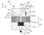
本実施の形態に係る半導体レーザは、図1Aに示すように、SiO2101上に、利得領域11と、リング共振器12と、DBR(Distributed Bragg Reflector)領域13と備える。
本実施の形態に係る半導体レーザ10の動作を、以下に説明する。
図3に、半導体レーザにおける発振ピーク波長と利得ピーク波長との温度依存性の計算結果を示す。
本発明の第2の実施の形態に係る半導体レーザについて、図4を参照して説明する。
本実施の形態に係る半導体レーザ20は、図4に示すように、SiO2101上に、利得領域11と、リング共振器22と、DBR(Distributed Bragg Reflector)領域13と、ループミラー23とを備える。
112 第1の半導体層
113 活性層
114 第2の半導体層
115_1 p型半導体層
115_2 n型半導体層
12 反射器(リング共振器)
131 回折格子
132 導波路層
16 屈折率制御部
Claims (9)
- 半導体レーザであって、
順に、第1の半導体層と、活性層と、第2の半導体層とを備える導波路構造と、
前記活性層の一方の側面に接して配置されるp型半導体層と、
前記活性層の他方の側面に接して配置されるn型半導体層と、
前記活性層の導波方向の一端に光学的に結合される反射器と、
前記活性層の導波方向の他端に光学的に結合される導波路層と、
前記導波路層の下面と上面とのいずれか一方に配置される回折格子と、
前記導波路層の屈折率を変化させる屈折率制御部と
を備え、
前記屈折率制御部により前記導波路層の屈折率が変化し、前記導波路層のブラッグ波長が長波長側にシフトし、前記導波路層のブラッグ波長と、前記反射器の長波長側の共振波長とが、前記半導体レーザの温度が増加するときに長波長側にシフトする前記活性層の利得ピークに一致し発振する
ことを特徴とする半導体レーザ。 - 前記反射器が複数のモードの発振光を発生させ、
前記屈折率制御部がオフの状態で、前記複数のモードの発振光のうち、所定の波長の前記発振光が、前記回折格子により選択され発振し、
前記屈折率制御部がオンの状態で、前記複数のモードの発振光のうち、所定の波長より長波長側の前記発振光が、前記回折格子により選択され発振する
ことを特徴とする請求項1に記載の半導体レーザ。 - 前記反射器が、リング共振器である
ことを特徴とする請求項1又は請求項2に記載の半導体レーザ。 - 前記リング共振器に光学的に結合するループミラーを備える
ことを特徴とする請求項3に記載の半導体レーザ。 - 前記リング共振器に光学的に結合し、一方の端部に回折格子を有する導波路を備える
ことを特徴とする請求項3に記載の半導体レーザ。 - 前記反射器が、サンプルド・グレーティングを有する導波路である
ことを特徴とする請求項1又は請求項2に記載の半導体レーザ。 - 前記屈折率制御部が、ヒータである
ことを特徴とする請求項1から請求項6のいずれか一項に記載の半導体レーザ。 - 前記屈折率制御部が、電源に接続され、前記導波路層に配置される電極であって、前記電極にバイアスを印加して、前記導波路層のキャリア密度を変化させる
ことを特徴とする請求項1から請求項6のいずれか一項に記載の半導体レーザ。 - 活性層と、前記活性層の導波方向の一端に光学的に結合される反射器と、前記活性層の導波方向の他端に光学的に結合され、回折格子を有する導波路層と、前記導波路層の屈折率を変化させる屈折率制御部とを備える半導体レーザの制御方法であって、
前記屈折率制御部により前記導波路層の屈折率を変化させ、前記導波路層のブラッグ波長を長波長側にシフトさせ、前記導波路層のブラッグ波長と、前記反射器の長波長側の共振波長とを、前記半導体レーザの温度が増加するときに長波長側にシフトする前記活性層の利得ピークに一致させ発振させる
ことを特徴とする半導体レーザの制御方法。
Applications Claiming Priority (1)
| Application Number | Priority Date | Filing Date | Title |
|---|---|---|---|
| PCT/JP2021/047031 WO2023119366A1 (ja) | 2021-12-20 | 2021-12-20 | 半導体レーザ |
Publications (2)
| Publication Number | Publication Date |
|---|---|
| JPWO2023119366A1 JPWO2023119366A1 (ja) | 2023-06-29 |
| JP7655404B2 true JP7655404B2 (ja) | 2025-04-02 |
Family
ID=86901569
Family Applications (1)
| Application Number | Title | Priority Date | Filing Date |
|---|---|---|---|
| JP2023568777A Active JP7655404B2 (ja) | 2021-12-20 | 2021-12-20 | 半導体レーザ |
Country Status (3)
| Country | Link |
|---|---|
| US (1) | US20250055254A1 (ja) |
| JP (1) | JP7655404B2 (ja) |
| WO (1) | WO2023119366A1 (ja) |
Families Citing this family (1)
| Publication number | Priority date | Publication date | Assignee | Title |
|---|---|---|---|---|
| CN120709817B (zh) * | 2025-09-01 | 2025-11-28 | 苏州实验室 | 弯曲波导面发射半导体激光器 |
Citations (6)
| Publication number | Priority date | Publication date | Assignee | Title |
|---|---|---|---|---|
| US20100260220A1 (en) | 2009-03-26 | 2010-10-14 | Gideon Yoffe | Semiconductor laser device and circuit for and method of driving same |
| JP2012256667A (ja) | 2011-06-08 | 2012-12-27 | Nippon Telegr & Teleph Corp <Ntt> | 半導体レーザ光源 |
| JP2016152360A (ja) | 2015-02-18 | 2016-08-22 | 富士通株式会社 | 光半導体装置 |
| JP2016178283A (ja) | 2015-03-20 | 2016-10-06 | 古河電気工業株式会社 | 波長可変レーザ素子およびレーザモジュール |
| JP2017168545A (ja) | 2016-03-15 | 2017-09-21 | 富士通株式会社 | 光モジュール |
| JP2017204601A (ja) | 2016-05-13 | 2017-11-16 | 日本電信電話株式会社 | 半導体レーザ |
-
2021
- 2021-12-20 JP JP2023568777A patent/JP7655404B2/ja active Active
- 2021-12-20 WO PCT/JP2021/047031 patent/WO2023119366A1/ja not_active Ceased
- 2021-12-20 US US18/721,626 patent/US20250055254A1/en active Pending
Patent Citations (6)
| Publication number | Priority date | Publication date | Assignee | Title |
|---|---|---|---|---|
| US20100260220A1 (en) | 2009-03-26 | 2010-10-14 | Gideon Yoffe | Semiconductor laser device and circuit for and method of driving same |
| JP2012256667A (ja) | 2011-06-08 | 2012-12-27 | Nippon Telegr & Teleph Corp <Ntt> | 半導体レーザ光源 |
| JP2016152360A (ja) | 2015-02-18 | 2016-08-22 | 富士通株式会社 | 光半導体装置 |
| JP2016178283A (ja) | 2015-03-20 | 2016-10-06 | 古河電気工業株式会社 | 波長可変レーザ素子およびレーザモジュール |
| JP2017168545A (ja) | 2016-03-15 | 2017-09-21 | 富士通株式会社 | 光モジュール |
| JP2017204601A (ja) | 2016-05-13 | 2017-11-16 | 日本電信電話株式会社 | 半導体レーザ |
Also Published As
| Publication number | Publication date |
|---|---|
| WO2023119366A1 (ja) | 2023-06-29 |
| JPWO2023119366A1 (ja) | 2023-06-29 |
| US20250055254A1 (en) | 2025-02-13 |
Similar Documents
| Publication | Publication Date | Title |
|---|---|---|
| US10193305B2 (en) | Wavelength tunable laser device and laser module | |
| US8615025B2 (en) | Method and system for hybrid integration of a tunable laser | |
| Spott et al. | Heterogeneous integration for mid-infrared silicon photonics | |
| US9318868B2 (en) | Tunable hybrid laser with carrier-induced phase control | |
| US8605766B2 (en) | Method and system for hybrid integration of a tunable laser and a mach zehnder modulator | |
| US8559470B2 (en) | Method and system for hybrid integration of a tunable laser and a phase modulator | |
| CN104937791B (zh) | 激光装置、光调制装置以及光半导体元件 | |
| US8576472B2 (en) | Optoelectronic device with controlled temperature dependence of the emission wavelength and method of making same | |
| WO2016152274A1 (ja) | 波長可変レーザ素子およびレーザモジュール | |
| WO2005053124A1 (ja) | 分布帰還型半導体レーザ、分布帰還型半導体レーザアレイ及び光モジュール | |
| JP5001239B2 (ja) | 半導体波長可変レーザ | |
| KR100216959B1 (ko) | 레이저 구조 | |
| JP7719999B2 (ja) | 半導体レーザ | |
| WO2023119366A1 (ja) | 半導体レーザ | |
| JP2011086714A (ja) | 波長可変レーザ | |
| KR100626270B1 (ko) | 광 대역 파장 가변 결합 링 반사기 레이저 다이오드 | |
| US20250047068A1 (en) | Distributed feedback lasers and methods for fabricating such lasers | |
| US20230296841A1 (en) | Optical component | |
| JP2004296560A (ja) | 半導体レーザの製造方法および集積光回路の製造方法 | |
| US20050226283A1 (en) | Single-mode semiconductor laser with integrated optical waveguide filter | |
| JP5058087B2 (ja) | 波長可変半導体レーザ | |
| JP7294453B2 (ja) | 直接変調レーザ | |
| JP2018046144A (ja) | 波長可変レーザ、波長可変レーザ装置及びその制御方法 | |
| WO2022130622A1 (ja) | 光デバイス | |
| US12603476B2 (en) | Extended-cavity diode laser component and method for producing same |
Legal Events
| Date | Code | Title | Description |
|---|---|---|---|
| A621 | Written request for application examination |
Free format text: JAPANESE INTERMEDIATE CODE: A621 Effective date: 20240531 |
|
| A131 | Notification of reasons for refusal |
Free format text: JAPANESE INTERMEDIATE CODE: A131 Effective date: 20241210 |
|
| A521 | Request for written amendment filed |
Free format text: JAPANESE INTERMEDIATE CODE: A523 Effective date: 20250206 |
|
| TRDD | Decision of grant or rejection written | ||
| A01 | Written decision to grant a patent or to grant a registration (utility model) |
Free format text: JAPANESE INTERMEDIATE CODE: A01 Effective date: 20250218 |
|
| A61 | First payment of annual fees (during grant procedure) |
Free format text: JAPANESE INTERMEDIATE CODE: A61 Effective date: 20250303 |
|
| R150 | Certificate of patent or registration of utility model |
Ref document number: 7655404 Country of ref document: JP Free format text: JAPANESE INTERMEDIATE CODE: R150 |
|
| S533 | Written request for registration of change of name |
Free format text: JAPANESE INTERMEDIATE CODE: R313533 |
|
| R350 | Written notification of registration of transfer |
Free format text: JAPANESE INTERMEDIATE CODE: R350 |