JP7670848B2 - 3次元のメモリデバイスおよびそれを形成するための方法 - Google Patents
3次元のメモリデバイスおよびそれを形成するための方法 Download PDFInfo
- Publication number
- JP7670848B2 JP7670848B2 JP2023555822A JP2023555822A JP7670848B2 JP 7670848 B2 JP7670848 B2 JP 7670848B2 JP 2023555822 A JP2023555822 A JP 2023555822A JP 2023555822 A JP2023555822 A JP 2023555822A JP 7670848 B2 JP7670848 B2 JP 7670848B2
- Authority
- JP
- Japan
- Prior art keywords
- layer
- channel
- doped
- semiconductor
- memory device
- Prior art date
- Legal status (The legal status is an assumption and is not a legal conclusion. Google has not performed a legal analysis and makes no representation as to the accuracy of the status listed.)
- Active
Links
Images


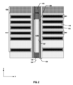


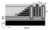


Classifications
-
- H—ELECTRICITY
- H10—SEMICONDUCTOR DEVICES; ELECTRIC SOLID-STATE DEVICES NOT OTHERWISE PROVIDED FOR
- H10B—ELECTRONIC MEMORY DEVICES
- H10B41/00—Electrically erasable-and-programmable ROM [EEPROM] devices comprising floating gates
- H10B41/20—Electrically erasable-and-programmable ROM [EEPROM] devices comprising floating gates characterised by three-dimensional [3D] arrangements, e.g. with cells on different height levels
- H10B41/23—Electrically erasable-and-programmable ROM [EEPROM] devices comprising floating gates characterised by three-dimensional [3D] arrangements, e.g. with cells on different height levels with source and drain on different levels, e.g. with sloping channels
- H10B41/27—Electrically erasable-and-programmable ROM [EEPROM] devices comprising floating gates characterised by three-dimensional [3D] arrangements, e.g. with cells on different height levels with source and drain on different levels, e.g. with sloping channels the channels comprising vertical portions, e.g. U-shaped channels
-
- H—ELECTRICITY
- H10—SEMICONDUCTOR DEVICES; ELECTRIC SOLID-STATE DEVICES NOT OTHERWISE PROVIDED FOR
- H10B—ELECTRONIC MEMORY DEVICES
- H10B41/00—Electrically erasable-and-programmable ROM [EEPROM] devices comprising floating gates
- H10B41/30—Electrically erasable-and-programmable ROM [EEPROM] devices comprising floating gates characterised by the memory core region
- H10B41/35—Electrically erasable-and-programmable ROM [EEPROM] devices comprising floating gates characterised by the memory core region with a cell select transistor, e.g. NAND
-
- H—ELECTRICITY
- H10—SEMICONDUCTOR DEVICES; ELECTRIC SOLID-STATE DEVICES NOT OTHERWISE PROVIDED FOR
- H10B—ELECTRONIC MEMORY DEVICES
- H10B41/00—Electrically erasable-and-programmable ROM [EEPROM] devices comprising floating gates
- H10B41/40—Electrically erasable-and-programmable ROM [EEPROM] devices comprising floating gates characterised by the peripheral circuit region
-
- H—ELECTRICITY
- H10—SEMICONDUCTOR DEVICES; ELECTRIC SOLID-STATE DEVICES NOT OTHERWISE PROVIDED FOR
- H10B—ELECTRONIC MEMORY DEVICES
- H10B43/00—EEPROM devices comprising charge-trapping gate insulators
- H10B43/20—EEPROM devices comprising charge-trapping gate insulators characterised by three-dimensional [3D] arrangements, e.g. with cells on different height levels
- H10B43/23—EEPROM devices comprising charge-trapping gate insulators characterised by three-dimensional [3D] arrangements, e.g. with cells on different height levels with source and drain on different levels, e.g. with sloping channels
- H10B43/27—EEPROM devices comprising charge-trapping gate insulators characterised by three-dimensional [3D] arrangements, e.g. with cells on different height levels with source and drain on different levels, e.g. with sloping channels the channels comprising vertical portions, e.g. U-shaped channels
-
- H—ELECTRICITY
- H10—SEMICONDUCTOR DEVICES; ELECTRIC SOLID-STATE DEVICES NOT OTHERWISE PROVIDED FOR
- H10B—ELECTRONIC MEMORY DEVICES
- H10B43/00—EEPROM devices comprising charge-trapping gate insulators
- H10B43/30—EEPROM devices comprising charge-trapping gate insulators characterised by the memory core region
- H10B43/35—EEPROM devices comprising charge-trapping gate insulators characterised by the memory core region with cell select transistors, e.g. NAND
-
- H—ELECTRICITY
- H10—SEMICONDUCTOR DEVICES; ELECTRIC SOLID-STATE DEVICES NOT OTHERWISE PROVIDED FOR
- H10B—ELECTRONIC MEMORY DEVICES
- H10B43/00—EEPROM devices comprising charge-trapping gate insulators
- H10B43/40—EEPROM devices comprising charge-trapping gate insulators characterised by the peripheral circuit region
-
- H—ELECTRICITY
- H10—SEMICONDUCTOR DEVICES; ELECTRIC SOLID-STATE DEVICES NOT OTHERWISE PROVIDED FOR
- H10B—ELECTRONIC MEMORY DEVICES
- H10B43/00—EEPROM devices comprising charge-trapping gate insulators
- H10B43/50—EEPROM devices comprising charge-trapping gate insulators characterised by the boundary region between the core and peripheral circuit regions
-
- H—ELECTRICITY
- H10—SEMICONDUCTOR DEVICES; ELECTRIC SOLID-STATE DEVICES NOT OTHERWISE PROVIDED FOR
- H10W—GENERIC PACKAGES, INTERCONNECTIONS, CONNECTORS OR OTHER CONSTRUCTIONAL DETAILS OF DEVICES COVERED BY CLASS H10
- H10W90/00—Package configurations
- H10W90/701—Package configurations characterised by the relative positions of pads or connectors relative to package parts
- H10W90/791—Package configurations characterised by the relative positions of pads or connectors relative to package parts of direct-bonded pads
- H10W90/792—Package configurations characterised by the relative positions of pads or connectors relative to package parts of direct-bonded pads between multiple chips
Landscapes
- Semiconductor Memories (AREA)
- Non-Volatile Memory (AREA)
- Metal-Oxide And Bipolar Metal-Oxide Semiconductor Integrated Circuits (AREA)
- Design And Manufacture Of Integrated Circuits (AREA)
Priority Applications (1)
| Application Number | Priority Date | Filing Date | Title |
|---|---|---|---|
| JP2025066245A JP2025114583A (ja) | 2021-03-22 | 2025-04-14 | 3次元のメモリデバイスおよびそれを形成するための方法 |
Applications Claiming Priority (1)
| Application Number | Priority Date | Filing Date | Title |
|---|---|---|---|
| PCT/CN2021/082028 WO2022198369A1 (en) | 2021-03-22 | 2021-03-22 | Three-dimensional memory devices and methods for forming the same |
Related Child Applications (1)
| Application Number | Title | Priority Date | Filing Date |
|---|---|---|---|
| JP2025066245A Division JP2025114583A (ja) | 2021-03-22 | 2025-04-14 | 3次元のメモリデバイスおよびそれを形成するための方法 |
Publications (2)
| Publication Number | Publication Date |
|---|---|
| JP2024510223A JP2024510223A (ja) | 2024-03-06 |
| JP7670848B2 true JP7670848B2 (ja) | 2025-04-30 |
Family
ID=79016674
Family Applications (2)
| Application Number | Title | Priority Date | Filing Date |
|---|---|---|---|
| JP2023555822A Active JP7670848B2 (ja) | 2021-03-22 | 2021-03-22 | 3次元のメモリデバイスおよびそれを形成するための方法 |
| JP2025066245A Pending JP2025114583A (ja) | 2021-03-22 | 2025-04-14 | 3次元のメモリデバイスおよびそれを形成するための方法 |
Family Applications After (1)
| Application Number | Title | Priority Date | Filing Date |
|---|---|---|---|
| JP2025066245A Pending JP2025114583A (ja) | 2021-03-22 | 2025-04-14 | 3次元のメモリデバイスおよびそれを形成するための方法 |
Country Status (7)
| Country | Link |
|---|---|
| US (2) | US12310011B2 (de) |
| EP (1) | EP4282004A4 (de) |
| JP (2) | JP7670848B2 (de) |
| KR (2) | KR102944271B1 (de) |
| CN (2) | CN113892179B (de) |
| TW (1) | TWI788837B (de) |
| WO (1) | WO2022198369A1 (de) |
Families Citing this family (14)
| Publication number | Priority date | Publication date | Assignee | Title |
|---|---|---|---|---|
| JP2022041054A (ja) | 2020-08-31 | 2022-03-11 | キオクシア株式会社 | 半導体記憶装置 |
| US11810838B2 (en) * | 2021-06-30 | 2023-11-07 | Micron Technology, Inc. | Microelectronic devices, and related electronic systems and methods of forming microelectronic devices |
| US11996377B2 (en) | 2021-06-30 | 2024-05-28 | Micron Technology, Inc. | Microelectronic devices and electronic systems |
| US11842990B2 (en) | 2021-06-30 | 2023-12-12 | Micron Technology, Inc. | Microelectronic devices and electronic systems |
| US11785764B2 (en) | 2021-06-30 | 2023-10-10 | Micron Technology, Inc. | Methods of forming microelectronic devices |
| US11776925B2 (en) | 2021-06-30 | 2023-10-03 | Micron Technology, Inc. | Methods of forming microelectronic devices, and related microelectronic devices and electronic systems |
| US11837594B2 (en) | 2021-06-30 | 2023-12-05 | Micron Technology, Inc. | Microelectronic devices and electronic systems |
| US11930634B2 (en) | 2021-06-30 | 2024-03-12 | Micron Technology, Inc. | Methods of forming microelectronic devices |
| US11751383B2 (en) | 2021-08-31 | 2023-09-05 | Micron Technology, Inc. | Methods of forming microelectronic devices, and related microelectronic devices and electronic systems |
| JP2023037973A (ja) * | 2021-09-06 | 2023-03-16 | キオクシア株式会社 | 半導体記憶装置 |
| US12200932B2 (en) * | 2021-11-22 | 2025-01-14 | Sandisk Technologies Llc | Three-dimensional memory device and method of making the same using differential thinning of vertical channels |
| TWI877740B (zh) | 2022-10-11 | 2025-03-21 | 日商鎧俠股份有限公司 | 半導體裝置及其製造方法 |
| JP2025506939A (ja) | 2022-12-30 | 2025-03-13 | 長江存儲科技有限責任公司 | 3次元不揮発性メモリフロアプランアーキテクチャ |
| WO2025005997A1 (en) * | 2023-06-28 | 2025-01-02 | SanDisk Technologies, Inc. | Three-dimensional memory device including backside semiconductor source structure and methods for forming the same |
Citations (7)
| Publication number | Priority date | Publication date | Assignee | Title |
|---|---|---|---|---|
| US20130032878A1 (en) | 2011-08-03 | 2013-02-07 | Kim Bi-O | Semiconductor device |
| US20150200259A1 (en) | 2014-01-16 | 2015-07-16 | Samsung Electronics Co., Ltd. | Semiconductor device and method of manufacturing the same |
| US20180138193A1 (en) | 2016-11-17 | 2018-05-17 | Sandisk Technologies Llc | Three-dimensional memory device having a multilevel drain select gate electrode and method of making thereof |
| CN110800106A (zh) | 2019-09-29 | 2020-02-14 | 长江存储科技有限责任公司 | 具有外延生长的半导体沟道的三维存储器件及其形成方法 |
| US20200258816A1 (en) | 2019-02-13 | 2020-08-13 | Sandisk Technologies Llc | Bonded three-dimensional memory devices and methods of making the same by replacing carrier substrate with source layer |
| CN111758164A (zh) | 2020-04-14 | 2020-10-09 | 长江存储科技有限责任公司 | 三维存储器件和用于形成其的方法 |
| CN111801800A (zh) | 2020-05-27 | 2020-10-20 | 长江存储科技有限责任公司 | 三维存储器件 |
Family Cites Families (77)
| Publication number | Priority date | Publication date | Assignee | Title |
|---|---|---|---|---|
| JP5395460B2 (ja) | 2009-02-25 | 2014-01-22 | 株式会社東芝 | 不揮発性半導体記憶装置、及びその製造方法 |
| KR101624980B1 (ko) * | 2009-06-19 | 2016-05-27 | 삼성전자주식회사 | 비휘발성 메모리 소자 |
| KR20130037063A (ko) | 2011-10-05 | 2013-04-15 | 에스케이하이닉스 주식회사 | 3차원 구조의 비휘발성 메모리 소자 및 그 제조 방법 |
| KR20130076461A (ko) | 2011-12-28 | 2013-07-08 | 에스케이하이닉스 주식회사 | 비휘발성 메모리 장치 및 그 제조 방법 |
| US9099202B2 (en) | 2012-11-06 | 2015-08-04 | Sandisk Technologies Inc. | 3D stacked non-volatile storage programming to conductive state |
| US8846508B1 (en) * | 2013-07-15 | 2014-09-30 | Varian Semiconductor Equipment Associates, Inc. | Method of implanting high aspect ratio features |
| JP2015079802A (ja) | 2013-10-15 | 2015-04-23 | 株式会社東芝 | 不揮発性半導体記憶装置 |
| US9449983B2 (en) | 2013-12-19 | 2016-09-20 | Sandisk Technologies Llc | Three dimensional NAND device with channel located on three sides of lower select gate and method of making thereof |
| TWI577062B (zh) | 2014-06-16 | 2017-04-01 | 旺宏電子股份有限公司 | 記憶體元件及其製作方法 |
| US9356040B2 (en) | 2014-06-27 | 2016-05-31 | Macronix International Co., Ltd. | Junction formation for vertical gate 3D NAND memory |
| EP3231012B1 (de) | 2014-12-09 | 2023-09-20 | SanDisk Technologies LLC | Dreidimensionale speicherstruktur mit rück-gate-elektrode |
| US9711524B2 (en) * | 2015-01-13 | 2017-07-18 | Sandisk Technologies Llc | Three-dimensional memory device containing plural select gate transistors having different characteristics and method of making thereof |
| US9406693B1 (en) | 2015-04-20 | 2016-08-02 | Sandisk Technologies Llc | Selective removal of charge-trapping layer for select gate transistors and dummy memory cells in 3D stacked memory |
| US9917100B2 (en) | 2015-11-20 | 2018-03-13 | Sandisk Technologies Llc | Three-dimensional NAND device containing support pedestal structures for a buried source line and method of making the same |
| US10727947B2 (en) | 2016-01-05 | 2020-07-28 | Morton Photonics | Reflection engineering / wavelength division multiplexing (WDM) geometric optical isolator |
| KR102549452B1 (ko) | 2016-03-31 | 2023-06-30 | 에스케이하이닉스 주식회사 | 반도체 장치 및 그 제조 방법 |
| US9741737B1 (en) | 2016-04-15 | 2017-08-22 | Micron Technology, Inc. | Integrated structures comprising vertical channel material and having conductively-doped semiconductor material directly against lower sidewalls of the channel material |
| US9917093B2 (en) | 2016-06-28 | 2018-03-13 | Sandisk Technologies Llc | Inter-plane offset in backside contact via structures for a three-dimensional memory device |
| US9824966B1 (en) | 2016-08-12 | 2017-11-21 | Sandisk Technologies Llc | Three-dimensional memory device containing a lateral source contact and method of making the same |
| US9805805B1 (en) * | 2016-08-23 | 2017-10-31 | Sandisk Technologies Llc | Three-dimensional memory device with charge carrier injection wells for vertical channels and method of making and using thereof |
| US9941293B1 (en) | 2016-10-12 | 2018-04-10 | Sandisk Technologies Llc | Select transistors with tight threshold voltage in 3D memory |
| US10128265B2 (en) | 2017-01-18 | 2018-11-13 | Micron Technology, Inc. | Memory cells, integrated structures and memory arrays |
| US10256245B2 (en) | 2017-03-10 | 2019-04-09 | Sandisk Technologies Llc | Three-dimensional memory device with short-free source select gate contact via structure and method of making the same |
| KR102343847B1 (ko) | 2017-04-25 | 2021-12-28 | 삼성전자주식회사 | 3차원 반도체 메모리 장치 |
| KR102368932B1 (ko) | 2017-06-01 | 2022-03-02 | 삼성전자주식회사 | 반도체 메모리 장치 |
| US10438964B2 (en) | 2017-06-26 | 2019-10-08 | Sandisk Technologies Llc | Three-dimensional memory device having direct source contact and metal oxide blocking dielectric and method of making thereof |
| US10290645B2 (en) | 2017-06-30 | 2019-05-14 | Sandisk Technologies Llc | Three-dimensional memory device containing hydrogen diffusion barrier layer for CMOS under array architecture and method of making thereof |
| US10510957B2 (en) | 2017-07-26 | 2019-12-17 | Micron Technology, Inc. | Self-aligned memory decks in cross-point memory arrays |
| US10199359B1 (en) | 2017-08-04 | 2019-02-05 | Sandisk Technologies Llc | Three-dimensional memory device employing direct source contact and hole current detection and method of making the same |
| WO2019037403A1 (en) | 2017-08-21 | 2019-02-28 | Yangtze Memory Technologies Co., Ltd. | THREE-DIMENSIONAL STABLE MEMORY DEVICES AND METHODS OF FORMING THE SAME |
| CN109473441B (zh) | 2017-08-31 | 2021-08-31 | 长江存储科技有限责任公司 | 一种3d nand存储器存储单元结构 |
| TWI647819B (zh) | 2017-09-01 | 2019-01-11 | 旺宏電子股份有限公司 | 立體記憶體元件及其製作方法 |
| CN107658317B (zh) | 2017-09-15 | 2019-01-01 | 长江存储科技有限责任公司 | 一种半导体装置及其制备方法 |
| EP3711092A4 (de) | 2017-11-15 | 2020-12-02 | SanDisk Technologies LLC | Dreidimensionale speichervorrichtung mit verdickten wortleitungen in der terrassenregion und verfahren zu deren herstellung |
| CN107887395B (zh) | 2017-11-30 | 2018-12-14 | 长江存储科技有限责任公司 | Nand存储器及其制备方法 |
| US10720445B1 (en) | 2018-02-08 | 2020-07-21 | Sandisk Technologies Llc | Three-dimensional memory device having nitrided direct source strap contacts and method of making thereof |
| US10580783B2 (en) | 2018-03-01 | 2020-03-03 | Sandisk Technologies Llc | Multi-tier three-dimensional memory device containing differential etch rate field oxides and method of making the same |
| JP2019165135A (ja) | 2018-03-20 | 2019-09-26 | 東芝メモリ株式会社 | 半導体記憶装置 |
| CN109219885A (zh) | 2018-07-20 | 2019-01-15 | 长江存储科技有限责任公司 | 三维存储器件 |
| AU2018433803B2 (en) | 2018-07-27 | 2021-12-02 | Yangtze Memory Technologies Co., Ltd. | Multiple-stack three-dimensional memory device and fabrication method thereof |
| KR102550605B1 (ko) * | 2018-08-28 | 2023-07-04 | 에스케이하이닉스 주식회사 | 반도체 장치 및 그 제조방법 |
| US10553599B1 (en) | 2018-09-26 | 2020-02-04 | Sandisk Technologies Llc | Three-dimensional memory device containing drain select isolation structures and on-pitch channels and methods of making the same without an etch stop layer |
| US11018151B2 (en) | 2018-09-26 | 2021-05-25 | Sandisk Technologies Llc | Three-dimensional flat NAND memory device including wavy word lines and method of making the same |
| KR102541001B1 (ko) | 2018-09-28 | 2023-06-07 | 삼성전자주식회사 | 수직형 메모리 장치 |
| KR102644525B1 (ko) * | 2018-11-07 | 2024-03-07 | 삼성전자주식회사 | 수직형 반도체 소자 |
| CN109473445B (zh) | 2018-11-09 | 2021-01-29 | 中国科学院微电子研究所 | 存储器件及其制造方法及包括该存储器件的电子设备 |
| US10629613B1 (en) | 2018-11-20 | 2020-04-21 | Sandisk Technologies Llc | Three-dimensional memory device having vertical semiconductor channels including source-side boron-doped pockets and methods of making the same |
| CN111354739A (zh) * | 2018-12-21 | 2020-06-30 | 芯恩(青岛)集成电路有限公司 | 一种三维有结半导体存储器件及其制造方法 |
| US11183511B2 (en) | 2019-01-25 | 2021-11-23 | Macronix International Co., Ltd. | Memory device and manufacturing method for the same |
| JP2020141008A (ja) | 2019-02-27 | 2020-09-03 | キオクシア株式会社 | 半導体記憶装置及びその製造方法 |
| CN109755254A (zh) | 2019-02-28 | 2019-05-14 | 长江存储科技有限责任公司 | 三维存储器及其制作方法 |
| JP2020145233A (ja) | 2019-03-04 | 2020-09-10 | キオクシア株式会社 | 半導体装置およびその製造方法 |
| TWI681550B (zh) | 2019-03-14 | 2020-01-01 | 旺宏電子股份有限公司 | 立體記憶體元件及其製作方法 |
| CN110114880B (zh) * | 2019-03-29 | 2020-10-30 | 长江存储科技有限责任公司 | 具有氮化硅栅极到栅极电介质层的存储堆叠体及其形成方法 |
| KR102704111B1 (ko) * | 2019-05-31 | 2024-09-06 | 삼성전자주식회사 | 3차원 반도체 장치 및 그 제조방법 |
| CN110112134B (zh) | 2019-06-17 | 2020-05-19 | 长江存储科技有限责任公司 | 3d nand存储器及其形成方法 |
| CN110349971A (zh) | 2019-06-28 | 2019-10-18 | 长江存储科技有限责任公司 | 用于三维存储器的叠层结构、三维存储器及其制备方法 |
| US11018154B2 (en) | 2019-08-19 | 2021-05-25 | Macronix International Co., Ltd. | Memory device and method for fabricating the same |
| KR102216132B1 (ko) | 2019-08-26 | 2021-02-16 | 에스케이하이닉스 주식회사 | 반도체 장치 및 반도체 장치의 제조 방법 |
| US10985252B2 (en) | 2019-08-26 | 2021-04-20 | Micron Technology, Inc. | Integrated assemblies, and methods of forming integrated assemblies |
| JP2021034696A (ja) | 2019-08-29 | 2021-03-01 | キオクシア株式会社 | 半導体記憶装置 |
| CN111354730B (zh) | 2020-03-12 | 2023-04-11 | 长江存储科技有限责任公司 | 三维存储器及其制备方法 |
| CN111370423B (zh) | 2020-03-16 | 2023-01-17 | 长江存储科技有限责任公司 | 三维存储器及其制作方法 |
| EP4136675B1 (de) * | 2020-04-14 | 2025-07-16 | Yangtze Memory Technologies Co., Ltd. | Verfahren zur herstellung einer dreidimensionalen speichervorrichtung mit rückseitigem source-kontakt |
| CN112424933B (zh) | 2020-05-27 | 2024-05-28 | 长江存储科技有限责任公司 | 用于形成三维存储器件的方法 |
| WO2021237489A1 (en) | 2020-05-27 | 2021-12-02 | Yangtze Memory Technologies Co., Ltd. | Methods for forming three-dimensional memory devices |
| JP7297923B2 (ja) | 2020-05-27 | 2023-06-26 | 長江存儲科技有限責任公司 | 3次元メモリデバイス及び方法 |
| JP7273183B2 (ja) * | 2020-05-27 | 2023-05-12 | 長江存儲科技有限責任公司 | 3次元メモリデバイスを形成するための方法 |
| JP7305774B2 (ja) | 2020-05-27 | 2023-07-10 | 長江存儲科技有限責任公司 | 3次元メモリデバイス |
| CN111755453B (zh) | 2020-05-29 | 2021-06-04 | 长江存储科技有限责任公司 | 3d存储器件及其制造方法 |
| CN111799265B (zh) | 2020-06-30 | 2021-06-04 | 湘潭大学 | 一种三维nand型铁电场效应晶体管存储器及其制备方法 |
| KR102762111B1 (ko) * | 2020-07-30 | 2025-02-03 | 양쯔 메모리 테크놀로지스 씨오., 엘티디. | 수소가 풍부한 반도체 채널을 구비한 3차원 메모리 장치 |
| US11552100B2 (en) | 2020-08-05 | 2023-01-10 | Sandisk Technologies Llc | Three-dimensional memory device including a composite semiconductor channel and a horizontal source contact layer and method of making the same |
| CN112331652A (zh) | 2020-10-23 | 2021-02-05 | 长江存储科技有限责任公司 | 位线驱动结构及三维存储器结构 |
| US11626415B2 (en) * | 2021-02-16 | 2023-04-11 | Sandisk Technologies Llc | Lateral transistors for selecting blocks in a three-dimensional memory array and methods for forming the same |
| KR102856680B1 (ko) * | 2021-03-22 | 2025-09-05 | 양쯔 메모리 테크놀로지스 씨오., 엘티디. | 3차원 메모리 디바이스 및 이를 형성하기 위한 방법 |
| EP4282003A4 (de) * | 2021-03-22 | 2024-08-28 | Yangtze Memory Technologies Co., Ltd. | Dreidimensionale speichervorrichtungen und verfahren zur formung davon |
-
2021
- 2021-03-22 KR KR1020237030434A patent/KR102944271B1/ko active Active
- 2021-03-22 CN CN202180000914.6A patent/CN113892179B/zh active Active
- 2021-03-22 JP JP2023555822A patent/JP7670848B2/ja active Active
- 2021-03-22 EP EP21932004.1A patent/EP4282004A4/de active Pending
- 2021-03-22 CN CN202610751087.9A patent/CN122555160A/zh active Pending
- 2021-03-22 KR KR1020267008266A patent/KR20260044257A/ko active Pending
- 2021-03-22 WO PCT/CN2021/082028 patent/WO2022198369A1/en not_active Ceased
- 2021-05-07 TW TW110116523A patent/TWI788837B/zh active
- 2021-06-18 US US17/352,242 patent/US12310011B2/en active Active
-
2024
- 2024-05-28 US US18/676,298 patent/US12701700B2/en active Active
-
2025
- 2025-04-14 JP JP2025066245A patent/JP2025114583A/ja active Pending
Patent Citations (7)
| Publication number | Priority date | Publication date | Assignee | Title |
|---|---|---|---|---|
| US20130032878A1 (en) | 2011-08-03 | 2013-02-07 | Kim Bi-O | Semiconductor device |
| US20150200259A1 (en) | 2014-01-16 | 2015-07-16 | Samsung Electronics Co., Ltd. | Semiconductor device and method of manufacturing the same |
| US20180138193A1 (en) | 2016-11-17 | 2018-05-17 | Sandisk Technologies Llc | Three-dimensional memory device having a multilevel drain select gate electrode and method of making thereof |
| US20200258816A1 (en) | 2019-02-13 | 2020-08-13 | Sandisk Technologies Llc | Bonded three-dimensional memory devices and methods of making the same by replacing carrier substrate with source layer |
| CN110800106A (zh) | 2019-09-29 | 2020-02-14 | 长江存储科技有限责任公司 | 具有外延生长的半导体沟道的三维存储器件及其形成方法 |
| CN111758164A (zh) | 2020-04-14 | 2020-10-09 | 长江存储科技有限责任公司 | 三维存储器件和用于形成其的方法 |
| CN111801800A (zh) | 2020-05-27 | 2020-10-20 | 长江存储科技有限责任公司 | 三维存储器件 |
Also Published As
| Publication number | Publication date |
|---|---|
| TWI788837B (zh) | 2023-01-01 |
| EP4282004A1 (de) | 2023-11-29 |
| KR20230138028A (ko) | 2023-10-05 |
| KR102944271B1 (ko) | 2026-03-25 |
| US12310011B2 (en) | 2025-05-20 |
| WO2022198369A1 (en) | 2022-09-29 |
| TW202238945A (zh) | 2022-10-01 |
| CN113892179B (zh) | 2026-06-16 |
| CN122555160A (zh) | 2026-08-11 |
| KR20260044257A (ko) | 2026-04-01 |
| JP2025114583A (ja) | 2025-08-05 |
| JP2024510223A (ja) | 2024-03-06 |
| US12701700B2 (en) | 2026-08-04 |
| US20240334690A1 (en) | 2024-10-03 |
| EP4282004A4 (de) | 2024-11-27 |
| US20220302150A1 (en) | 2022-09-22 |
| CN113892179A (zh) | 2022-01-04 |
Similar Documents
| Publication | Publication Date | Title |
|---|---|---|
| JP7633425B2 (ja) | 3次元のメモリデバイスおよびそれを形成するための方法 | |
| JP7652922B2 (ja) | 3次元のメモリデバイスおよびそれを形成するための方法 | |
| US12310011B2 (en) | Three-dimensional memory devices and methods for forming the same | |
| US12477749B2 (en) | Three-dimensional memory devices having semiconductor assemblies bonded by bonding layer and methods for forming the same | |
| US20230005944A1 (en) | Three-dimensional memory devices and methods for forming the same | |
| US11935862B2 (en) | Three-dimensional memory devices and methods for forming the same | |
| US20250056793A1 (en) | Managing three-dimensional semiconductive devices |
Legal Events
| Date | Code | Title | Description |
|---|---|---|---|
| A521 | Request for written amendment filed |
Free format text: JAPANESE INTERMEDIATE CODE: A523 Effective date: 20230912 |
|
| A621 | Written request for application examination |
Free format text: JAPANESE INTERMEDIATE CODE: A621 Effective date: 20230912 |
|
| A977 | Report on retrieval |
Free format text: JAPANESE INTERMEDIATE CODE: A971007 Effective date: 20240830 |
|
| A131 | Notification of reasons for refusal |
Free format text: JAPANESE INTERMEDIATE CODE: A131 Effective date: 20240909 |
|
| A521 | Request for written amendment filed |
Free format text: JAPANESE INTERMEDIATE CODE: A523 Effective date: 20241206 |
|
| TRDD | Decision of grant or rejection written | ||
| A01 | Written decision to grant a patent or to grant a registration (utility model) |
Free format text: JAPANESE INTERMEDIATE CODE: A01 Effective date: 20250318 |
|
| A61 | First payment of annual fees (during grant procedure) |
Free format text: JAPANESE INTERMEDIATE CODE: A61 Effective date: 20250417 |
|
| R150 | Certificate of patent or registration of utility model |
Ref document number: 7670848 Country of ref document: JP Free format text: JAPANESE INTERMEDIATE CODE: R150 |