JP7677004B2 - 照明光学系および露光装置 - Google Patents
照明光学系および露光装置 Download PDFInfo
- Publication number
- JP7677004B2 JP7677004B2 JP2021113402A JP2021113402A JP7677004B2 JP 7677004 B2 JP7677004 B2 JP 7677004B2 JP 2021113402 A JP2021113402 A JP 2021113402A JP 2021113402 A JP2021113402 A JP 2021113402A JP 7677004 B2 JP7677004 B2 JP 7677004B2
- Authority
- JP
- Japan
- Prior art keywords
- light
- lens
- optical system
- elements
- illumination optical
- Prior art date
- Legal status (The legal status is an assumption and is not a legal conclusion. Google has not performed a legal analysis and makes no representation as to the accuracy of the status listed.)
- Active
Links
Images




Classifications
-
- F—MECHANICAL ENGINEERING; LIGHTING; HEATING; WEAPONS; BLASTING
- F21—LIGHTING
- F21V—FUNCTIONAL FEATURES OR DETAILS OF LIGHTING DEVICES OR SYSTEMS THEREOF; STRUCTURAL COMBINATIONS OF LIGHTING DEVICES WITH OTHER ARTICLES, NOT OTHERWISE PROVIDED FOR
- F21V5/00—Refractors for light sources
- F21V5/02—Refractors for light sources of prismatic shape
-
- G—PHYSICS
- G02—OPTICS
- G02B—OPTICAL ELEMENTS, SYSTEMS OR APPARATUS
- G02B19/00—Condensers, e.g. light collectors or similar non-imaging optics
- G02B19/0004—Condensers, e.g. light collectors or similar non-imaging optics characterised by the optical means employed
- G02B19/0009—Condensers, e.g. light collectors or similar non-imaging optics characterised by the optical means employed having refractive surfaces only
- G02B19/0014—Condensers, e.g. light collectors or similar non-imaging optics characterised by the optical means employed having refractive surfaces only at least one surface having optical power
-
- G—PHYSICS
- G03—PHOTOGRAPHY; CINEMATOGRAPHY; ANALOGOUS TECHNIQUES USING WAVES OTHER THAN OPTICAL WAVES; ELECTROGRAPHY; HOLOGRAPHY
- G03F—PHOTOMECHANICAL PRODUCTION OF TEXTURED OR PATTERNED SURFACES, e.g. FOR PRINTING, FOR PROCESSING OF SEMICONDUCTOR DEVICES; MATERIALS THEREFOR; ORIGINALS THEREFOR; APPARATUS SPECIALLY ADAPTED THEREFOR
- G03F7/00—Photomechanical, e.g. photolithographic, production of textured or patterned surfaces, e.g. printing surfaces; Materials therefor, e.g. comprising photoresists; Apparatus specially adapted therefor
- G03F7/70—Microphotolithographic exposure; Apparatus therefor
- G03F7/70216—Mask projection systems
- G03F7/70308—Optical correction elements, filters or phase plates for manipulating imaging light, e.g. intensity, wavelength, polarisation, phase or image shift
-
- F—MECHANICAL ENGINEERING; LIGHTING; HEATING; WEAPONS; BLASTING
- F21—LIGHTING
- F21K—NON-ELECTRIC LIGHT SOURCES USING LUMINESCENCE; LIGHT SOURCES USING ELECTROCHEMILUMINESCENCE; LIGHT SOURCES USING CHARGES OF COMBUSTIBLE MATERIAL; LIGHT SOURCES USING SEMICONDUCTOR DEVICES AS LIGHT-GENERATING ELEMENTS; LIGHT SOURCES NOT OTHERWISE PROVIDED FOR
- F21K9/00—Light sources using semiconductor devices as light-generating elements, e.g. using light-emitting diodes [LED] or lasers
- F21K9/60—Optical arrangements integrated in the light source, e.g. for improving the colour rendering index or the light extraction
- F21K9/69—Details of refractors forming part of the light source
-
- F—MECHANICAL ENGINEERING; LIGHTING; HEATING; WEAPONS; BLASTING
- F21—LIGHTING
- F21V—FUNCTIONAL FEATURES OR DETAILS OF LIGHTING DEVICES OR SYSTEMS THEREOF; STRUCTURAL COMBINATIONS OF LIGHTING DEVICES WITH OTHER ARTICLES, NOT OTHERWISE PROVIDED FOR
- F21V5/00—Refractors for light sources
- F21V5/007—Array of lenses or refractors for a cluster of light sources, e.g. for arrangement of multiple light sources in one plane
-
- G—PHYSICS
- G02—OPTICS
- G02B—OPTICAL ELEMENTS, SYSTEMS OR APPARATUS
- G02B19/00—Condensers, e.g. light collectors or similar non-imaging optics
-
- G—PHYSICS
- G02—OPTICS
- G02B—OPTICAL ELEMENTS, SYSTEMS OR APPARATUS
- G02B19/00—Condensers, e.g. light collectors or similar non-imaging optics
- G02B19/0033—Condensers, e.g. light collectors or similar non-imaging optics characterised by the use
- G02B19/0047—Condensers, e.g. light collectors or similar non-imaging optics characterised by the use for use with a light source
- G02B19/0052—Condensers, e.g. light collectors or similar non-imaging optics characterised by the use for use with a light source the light source comprising a laser diode
-
- G—PHYSICS
- G02—OPTICS
- G02B—OPTICAL ELEMENTS, SYSTEMS OR APPARATUS
- G02B19/00—Condensers, e.g. light collectors or similar non-imaging optics
- G02B19/0033—Condensers, e.g. light collectors or similar non-imaging optics characterised by the use
- G02B19/0047—Condensers, e.g. light collectors or similar non-imaging optics characterised by the use for use with a light source
- G02B19/0052—Condensers, e.g. light collectors or similar non-imaging optics characterised by the use for use with a light source the light source comprising a laser diode
- G02B19/0057—Condensers, e.g. light collectors or similar non-imaging optics characterised by the use for use with a light source the light source comprising a laser diode in the form of a laser diode array, e.g. laser diode bar
-
- G—PHYSICS
- G02—OPTICS
- G02B—OPTICAL ELEMENTS, SYSTEMS OR APPARATUS
- G02B19/00—Condensers, e.g. light collectors or similar non-imaging optics
- G02B19/0033—Condensers, e.g. light collectors or similar non-imaging optics characterised by the use
- G02B19/0047—Condensers, e.g. light collectors or similar non-imaging optics characterised by the use for use with a light source
- G02B19/0061—Condensers, e.g. light collectors or similar non-imaging optics characterised by the use for use with a light source the light source comprising a LED
-
- G—PHYSICS
- G02—OPTICS
- G02B—OPTICAL ELEMENTS, SYSTEMS OR APPARATUS
- G02B19/00—Condensers, e.g. light collectors or similar non-imaging optics
- G02B19/0033—Condensers, e.g. light collectors or similar non-imaging optics characterised by the use
- G02B19/0047—Condensers, e.g. light collectors or similar non-imaging optics characterised by the use for use with a light source
- G02B19/0061—Condensers, e.g. light collectors or similar non-imaging optics characterised by the use for use with a light source the light source comprising a LED
- G02B19/0066—Condensers, e.g. light collectors or similar non-imaging optics characterised by the use for use with a light source the light source comprising a LED in the form of an LED array
-
- G—PHYSICS
- G02—OPTICS
- G02B—OPTICAL ELEMENTS, SYSTEMS OR APPARATUS
- G02B27/00—Optical systems or apparatus not provided for by any of the groups G02B1/00 - G02B26/00, G02B30/00
- G02B27/09—Beam shaping, e.g. changing the cross-sectional area, not otherwise provided for
- G02B27/0905—Dividing and/or superposing multiple light beams
-
- G—PHYSICS
- G02—OPTICS
- G02B—OPTICAL ELEMENTS, SYSTEMS OR APPARATUS
- G02B27/00—Optical systems or apparatus not provided for by any of the groups G02B1/00 - G02B26/00, G02B30/00
- G02B27/09—Beam shaping, e.g. changing the cross-sectional area, not otherwise provided for
- G02B27/0927—Systems for changing the beam intensity distribution, e.g. Gaussian to top-hat
-
- G—PHYSICS
- G02—OPTICS
- G02B—OPTICAL ELEMENTS, SYSTEMS OR APPARATUS
- G02B27/00—Optical systems or apparatus not provided for by any of the groups G02B1/00 - G02B26/00, G02B30/00
- G02B27/09—Beam shaping, e.g. changing the cross-sectional area, not otherwise provided for
- G02B27/0938—Using specific optical elements
- G02B27/095—Refractive optical elements
- G02B27/0955—Lenses
-
- G—PHYSICS
- G02—OPTICS
- G02B—OPTICAL ELEMENTS, SYSTEMS OR APPARATUS
- G02B27/00—Optical systems or apparatus not provided for by any of the groups G02B1/00 - G02B26/00, G02B30/00
- G02B27/09—Beam shaping, e.g. changing the cross-sectional area, not otherwise provided for
- G02B27/0938—Using specific optical elements
- G02B27/095—Refractive optical elements
- G02B27/0955—Lenses
- G02B27/0961—Lens arrays
-
- G—PHYSICS
- G02—OPTICS
- G02B—OPTICAL ELEMENTS, SYSTEMS OR APPARATUS
- G02B3/00—Simple or compound lenses
- G02B3/0006—Arrays
-
- G—PHYSICS
- G02—OPTICS
- G02B—OPTICAL ELEMENTS, SYSTEMS OR APPARATUS
- G02B3/00—Simple or compound lenses
- G02B3/0006—Arrays
- G02B3/0037—Arrays characterized by the distribution or form of lenses
- G02B3/0056—Arrays characterized by the distribution or form of lenses arranged along two different directions in a plane, e.g. honeycomb arrangement of lenses
-
- G—PHYSICS
- G02—OPTICS
- G02B—OPTICAL ELEMENTS, SYSTEMS OR APPARATUS
- G02B3/00—Simple or compound lenses
- G02B3/0006—Arrays
- G02B3/0037—Arrays characterized by the distribution or form of lenses
- G02B3/0062—Stacked lens arrays, i.e. refractive surfaces arranged in at least two planes, without structurally separate optical elements in-between
-
- G—PHYSICS
- G03—PHOTOGRAPHY; CINEMATOGRAPHY; ANALOGOUS TECHNIQUES USING WAVES OTHER THAN OPTICAL WAVES; ELECTROGRAPHY; HOLOGRAPHY
- G03F—PHOTOMECHANICAL PRODUCTION OF TEXTURED OR PATTERNED SURFACES, e.g. FOR PRINTING, FOR PROCESSING OF SEMICONDUCTOR DEVICES; MATERIALS THEREFOR; ORIGINALS THEREFOR; APPARATUS SPECIALLY ADAPTED THEREFOR
- G03F7/00—Photomechanical, e.g. photolithographic, production of textured or patterned surfaces, e.g. printing surfaces; Materials therefor, e.g. comprising photoresists; Apparatus specially adapted therefor
- G03F7/20—Exposure; Apparatus therefor
-
- G—PHYSICS
- G03—PHOTOGRAPHY; CINEMATOGRAPHY; ANALOGOUS TECHNIQUES USING WAVES OTHER THAN OPTICAL WAVES; ELECTROGRAPHY; HOLOGRAPHY
- G03F—PHOTOMECHANICAL PRODUCTION OF TEXTURED OR PATTERNED SURFACES, e.g. FOR PRINTING, FOR PROCESSING OF SEMICONDUCTOR DEVICES; MATERIALS THEREFOR; ORIGINALS THEREFOR; APPARATUS SPECIALLY ADAPTED THEREFOR
- G03F7/00—Photomechanical, e.g. photolithographic, production of textured or patterned surfaces, e.g. printing surfaces; Materials therefor, e.g. comprising photoresists; Apparatus specially adapted therefor
- G03F7/70—Microphotolithographic exposure; Apparatus therefor
- G03F7/70008—Production of exposure light, i.e. light sources
- G03F7/7005—Production of exposure light, i.e. light sources by multiple sources, e.g. light-emitting diodes [LED] or light source arrays
-
- G—PHYSICS
- G03—PHOTOGRAPHY; CINEMATOGRAPHY; ANALOGOUS TECHNIQUES USING WAVES OTHER THAN OPTICAL WAVES; ELECTROGRAPHY; HOLOGRAPHY
- G03F—PHOTOMECHANICAL PRODUCTION OF TEXTURED OR PATTERNED SURFACES, e.g. FOR PRINTING, FOR PROCESSING OF SEMICONDUCTOR DEVICES; MATERIALS THEREFOR; ORIGINALS THEREFOR; APPARATUS SPECIALLY ADAPTED THEREFOR
- G03F7/00—Photomechanical, e.g. photolithographic, production of textured or patterned surfaces, e.g. printing surfaces; Materials therefor, e.g. comprising photoresists; Apparatus specially adapted therefor
- G03F7/70—Microphotolithographic exposure; Apparatus therefor
- G03F7/70058—Mask illumination systems
- G03F7/70075—Homogenization of illumination intensity in the mask plane by using an integrator, e.g. fly's eye lens, facet mirror or glass rod, by using a diffusing optical element or by beam deflection
-
- G—PHYSICS
- G03—PHOTOGRAPHY; CINEMATOGRAPHY; ANALOGOUS TECHNIQUES USING WAVES OTHER THAN OPTICAL WAVES; ELECTROGRAPHY; HOLOGRAPHY
- G03F—PHOTOMECHANICAL PRODUCTION OF TEXTURED OR PATTERNED SURFACES, e.g. FOR PRINTING, FOR PROCESSING OF SEMICONDUCTOR DEVICES; MATERIALS THEREFOR; ORIGINALS THEREFOR; APPARATUS SPECIALLY ADAPTED THEREFOR
- G03F7/00—Photomechanical, e.g. photolithographic, production of textured or patterned surfaces, e.g. printing surfaces; Materials therefor, e.g. comprising photoresists; Apparatus specially adapted therefor
- G03F7/70—Microphotolithographic exposure; Apparatus therefor
- G03F7/70216—Mask projection systems
- G03F7/70316—Details of optical elements, e.g. of Bragg reflectors, extreme ultraviolet [EUV] multilayer or bilayer mirrors or diffractive optical elements
-
- G—PHYSICS
- G03—PHOTOGRAPHY; CINEMATOGRAPHY; ANALOGOUS TECHNIQUES USING WAVES OTHER THAN OPTICAL WAVES; ELECTROGRAPHY; HOLOGRAPHY
- G03F—PHOTOMECHANICAL PRODUCTION OF TEXTURED OR PATTERNED SURFACES, e.g. FOR PRINTING, FOR PROCESSING OF SEMICONDUCTOR DEVICES; MATERIALS THEREFOR; ORIGINALS THEREFOR; APPARATUS SPECIALLY ADAPTED THEREFOR
- G03F7/00—Photomechanical, e.g. photolithographic, production of textured or patterned surfaces, e.g. printing surfaces; Materials therefor, e.g. comprising photoresists; Apparatus specially adapted therefor
- G03F7/70—Microphotolithographic exposure; Apparatus therefor
- G03F7/70483—Information management; Active and passive control; Testing; Wafer monitoring, e.g. pattern monitoring
- G03F7/7055—Exposure light control in all parts of the microlithographic apparatus, e.g. pulse length control or light interruption
- G03F7/70583—Speckle reduction, e.g. coherence control or amplitude/wavefront splitting
-
- F—MECHANICAL ENGINEERING; LIGHTING; HEATING; WEAPONS; BLASTING
- F21—LIGHTING
- F21Y—INDEXING SCHEME ASSOCIATED WITH SUBCLASSES F21K, F21L, F21S and F21V, RELATING TO THE FORM OR THE KIND OF THE LIGHT SOURCES OR OF THE COLOUR OF THE LIGHT EMITTED
- F21Y2115/00—Light-generating elements of semiconductor light sources
Landscapes
- Physics & Mathematics (AREA)
- General Physics & Mathematics (AREA)
- Optics & Photonics (AREA)
- Engineering & Computer Science (AREA)
- General Engineering & Computer Science (AREA)
- Microelectronics & Electronic Packaging (AREA)
- Exposure And Positioning Against Photoresist Photosensitive Materials (AREA)
- Microscoopes, Condenser (AREA)
- Exposure Of Semiconductors, Excluding Electron Or Ion Beam Exposure (AREA)
Description
そこで、本発明は、複数の発光素子からの光を高い効率で利用することを目的とする。
集光レンズ群、レンズアレイ、およびリレーレンズによりリレー光学系の機能が分担され、リレー光学系が容易に実現される。
上記露光装置において、上記照明光学系によって照射された前記パターンの像を上記露光対象物に投影する投影光学系を備えてもよい。
図1は、本発明の照明光学系の一実施形態を示す図である。
図2は、本発明の露光装置の一実施形態を示す図である。
露光装置100には、照明光学系1と、マスクステージ110と、投影光学系120と、ワークステージ130が備えられている。
マスクステージ110はマスクMを保持し、そのマスクMには照明光学系1によって光が照射される。
ワークステージ130には、例えばガラス基板や半導体基板などといった露光対象となるワークWが保持される。
投影光学系120は、マスクMを透過した光をワークW上に投影してワークWをパターン露光する。
露光装置100は、投影光学系120を有さずに、ワークWがマスクMに近接あるいは接触して保持される方式のものであってもよい。
図1に戻って、リレー光学系20の詳細について説明する。
リレー光学系20は、一例として、集光レンズ群21と、レンズアレイ22と、リレーレンズ23とを有する。
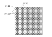
図3は、発光素子11と集光レンズ211とレンズ要素221との位置関係を示す図である。
複数の発光素子11はXY方向に配列されており、各発光素子11は四角い発光面を有している。
集光レンズ群21の集光レンズ211は、図1に示すいわゆる単玉レンズであってもよいが、例えば2枚のレンズによる組み合わせレンズであってもよい。
図4は、組み合わせレンズの集光レンズ211を示す図である。
図4には、側面図(A)と正面図(B)が示されている。
図4に示す集光レンズ211からなる集光レンズ群21が図3に示すレンズアレイ22と組み合わされることにより、図4に示す集光レンズ211からなる集光レンズ群21が図3に示すレンズアレイ22と組み合わされない場合(後述する比較例)と比較して光の利用効率が10%程度向上することが期待される。
再び図1に戻って説明を続ける。
図5は、発光素子11の配光特性を示す図である。
ここで、図1に示す実施形態における照度分布を比較例と比較して説明する。
比較例における照度分布は、被照射面において光の利用効率が最も良くなるよう設計された場合の照度分布である。
オプティカルインテグレータ30の入射面31全体での合計光量は、光源10における発光量を基準とした相対値で756.2となっている。
次に、本実施形態の照明光学系1に対する変形例について説明する。
図10および図11は、発光素子11、集光レンズ211、およびレンズ要素221の配置に関する変形例を示す図であり、マスクM(面)での照射形状が円形である場合の例である。
図10に示す丸い配置であっても、各集光レンズ211および各レンズ要素221が四角い外形を有することで光の利用効率が向上する。
各集光レンズ211および各レンズ要素221が丸い外形を有する変形例では、図3および図10に示す配置と較べると光の利用効率が低いが、発光素子11を点線で示した丸い範囲内に多く配置できる。また開口絞り40面でフラットな照度分布になるため図6、図7の比較例で開口絞り40の面で周辺までフラットな照度分布になるようにオプティカルインテグレータ30の入射面で照射範囲を広く設計した場合と比較すると光の利用効率が高くなる。
図12は、レンズアレイ22の構造が異なる変形例を示す図である。
図13は、リレー光学系20とオプティカルインテグレータ30との距離が異なる変形例を示す図である。
21…集光レンズ群、211…集光レンズ、212…前レンズ、213…後レンズ
22…レンズアレイ、221…レンズ要素、23…リレーレンズ、
30…オプティカルインテグレータ、31…入射面、32…波面分割要素、33…出射面
40…開口絞り、50…コンデンサレンズ、100…露光装置、
110…マスクステージ、120…投影光学系、130…ワークステージ
Claims (7)
- 各々が発光面から光を発する複数の発光素子が、当該発光面の広がる方向に互いに並んでいる光源と、
前記発光素子が発した光の配光分布を照度分布に変換すると共に、前記複数の発光素子に対応した複数の当該照度分布を重畳面上で互いに重ね合わせるリレー光学系と、
前記リレー光学系による照射光を波面分割して複数の光束として伝達する複数の波面分割要素が互いに並列的に配置されたオプティカルインテグレータと、
前記複数の光束を被照射面で重畳させるコンデンサ光学系と、
を備え、
前記リレー光学系が、
前記複数の発光素子に対応した複数の第1レンズ要素を有し、各第1レンズ要素が各発光素子からの光を集光する集光レンズ群と、
前記複数の第1レンズ要素に対応した複数の第2レンズ要素を有し、各発光素子からの光の配光分布に相当する照度分布の照射光が各第1レンズ要素により各第2レンズ要素の入射面に照射されるレンズアレイと、
前記レンズアレイの各第2レンズ要素の出射面と光学的に協働して、各第2レンズ要素の入射面に照射された各照射光を前記重畳面上に導いて互いに重ね合わせるリレーレンズと、
を備えたことを特徴とする照明光学系。 - 前記リレーレンズから前記オプティカルインテグレータの入射面までの距離は、当該リレーレンズから前記重畳面までの距離よりも短いことを特徴とする請求項1に記載の照明光学系。
- 前記レンズアレイは、前記複数の第2レンズ要素のそれぞれが、光軸に沿った方向に見て四角形の外形を有し、当該複数の第2レンズ要素が束ねられたことを特徴とする請求項1または2に記載の照明光学系。
- 前記集光レンズ群は、前記複数の第1レンズ要素のそれぞれの出射側が、光軸に沿った方向に見て四角形の外形を有し、当該複数の第1レンズ要素が束ねられたことを特徴とする請求項1または2に記載の照明光学系。
- 前記集光レンズ群は、前記複数の第1レンズ要素のそれぞれが、前記発光素子側に位置する前要素と前記レンズアレイ側に位置する後要素とを有し、当該前要素は光軸に沿った方向に見て丸い外形を有し、当該後要素は光軸に沿った方向に見て四角形の外形を有することを特徴とする請求項4に記載の照明光学系。
- 請求項1に記載の照明光学系で前記被照射面に配置されたパターンを照射して、当該パターンを露光対象物に露光することを特徴とする露光装置。
- 前記照明光学系によって照射された前記パターンの像を前記露光対象物に投影する投影光学系を備えたことを特徴とする請求項6に記載の露光装置。
Priority Applications (7)
| Application Number | Priority Date | Filing Date | Title |
|---|---|---|---|
| JP2021113402A JP7677004B2 (ja) | 2021-07-08 | 2021-07-08 | 照明光学系および露光装置 |
| KR1020237043662A KR102951745B1 (ko) | 2021-07-08 | 2022-03-24 | 조명 광학계 및 노광 장치 |
| US18/575,358 US12481220B2 (en) | 2021-07-08 | 2022-03-24 | Lighting optical system and exposure apparatus |
| PCT/JP2022/013874 WO2023281850A1 (ja) | 2021-07-08 | 2022-03-24 | 照明光学系および露光装置 |
| CN202280042886.9A CN117501183A (zh) | 2021-07-08 | 2022-03-24 | 照明光学系统及曝光装置 |
| EP22837272.8A EP4361701A4 (en) | 2021-07-08 | 2022-03-24 | OPTICAL ILLUMINATION SYSTEM AND EXPOSURE DEVICE |
| TW111114811A TWI905419B (zh) | 2021-07-08 | 2022-04-19 | 照明光學系統及曝光裝置 |
Applications Claiming Priority (1)
| Application Number | Priority Date | Filing Date | Title |
|---|---|---|---|
| JP2021113402A JP7677004B2 (ja) | 2021-07-08 | 2021-07-08 | 照明光学系および露光装置 |
Publications (2)
| Publication Number | Publication Date |
|---|---|
| JP2023009810A JP2023009810A (ja) | 2023-01-20 |
| JP7677004B2 true JP7677004B2 (ja) | 2025-05-15 |
Family
ID=84801657
Family Applications (1)
| Application Number | Title | Priority Date | Filing Date |
|---|---|---|---|
| JP2021113402A Active JP7677004B2 (ja) | 2021-07-08 | 2021-07-08 | 照明光学系および露光装置 |
Country Status (7)
| Country | Link |
|---|---|
| US (1) | US12481220B2 (ja) |
| EP (1) | EP4361701A4 (ja) |
| JP (1) | JP7677004B2 (ja) |
| KR (1) | KR102951745B1 (ja) |
| CN (1) | CN117501183A (ja) |
| TW (1) | TWI905419B (ja) |
| WO (1) | WO2023281850A1 (ja) |
Families Citing this family (1)
| Publication number | Priority date | Publication date | Assignee | Title |
|---|---|---|---|---|
| JP2025138162A (ja) | 2024-03-11 | 2025-09-25 | ウシオ電機株式会社 | 光源装置 |
Citations (7)
| Publication number | Priority date | Publication date | Assignee | Title |
|---|---|---|---|---|
| JP2001147305A (ja) | 1999-11-19 | 2001-05-29 | Seiko Epson Corp | マイクロレンズ用凹部付き基板の製造方法、マイクロレンズ基板、液晶パネル用対向基板、液晶パネルおよび投射型表示装置 |
| JP2003107400A (ja) | 2001-07-26 | 2003-04-09 | Ricoh Co Ltd | 画像表示装置 |
| JP2007025613A (ja) | 2004-09-03 | 2007-02-01 | Sanee Giken Kk | 露光用光源 |
| JP2012203417A (ja) | 2011-03-25 | 2012-10-22 | Min Aik Technology Co Ltd | 光混合装置、光混合方法及び該光混合装置を応用した小型投影システム |
| JP2016188878A (ja) | 2015-03-28 | 2016-11-04 | 株式会社ニコン | 照明光学系、露光装置、およびデバイス製造方法 |
| JP2020122921A (ja) | 2019-01-31 | 2020-08-13 | キヤノン株式会社 | 光源装置、照明装置、露光装置及び物品の製造方法 |
| JP2021189397A (ja) | 2020-06-04 | 2021-12-13 | キヤノン株式会社 | 露光装置、露光方法、及び物品の製造方法 |
Family Cites Families (12)
| Publication number | Priority date | Publication date | Assignee | Title |
|---|---|---|---|---|
| US5815248A (en) * | 1993-04-22 | 1998-09-29 | Nikon Corporation | Illumination optical apparatus and method having a wavefront splitter and an optical integrator |
| US5822125A (en) * | 1996-12-20 | 1998-10-13 | Eastman Kodak Company | Lenslet array system |
| JP3101613B2 (ja) * | 1998-01-30 | 2000-10-23 | キヤノン株式会社 | 照明光学装置及び投影露光装置 |
| JP3599629B2 (ja) * | 2000-03-06 | 2004-12-08 | キヤノン株式会社 | 照明光学系及び前記照明光学系を用いた露光装置 |
| WO2011012148A1 (en) * | 2009-07-31 | 2011-02-03 | Carl Zeiss Smt Gmbh | Optical beam deflecting element and method of adjustment |
| JP2011216863A (ja) * | 2010-03-17 | 2011-10-27 | Hitachi Via Mechanics Ltd | ビームサイズ可変照明光学装置及びビームサイズ変更方法 |
| JP2014003086A (ja) * | 2012-06-15 | 2014-01-09 | Ushio Inc | 光照射装置、露光装置 |
| CN102854632A (zh) * | 2012-08-16 | 2013-01-02 | 芜湖雅图数字视频技术有限公司 | 激光光源准直装置、准直装置阵列及照明系统和投影设备 |
| KR101633176B1 (ko) | 2014-05-14 | 2016-07-01 | 주은유브이텍 주식회사 | 자외선 엘이디 모듈 및 이를 포함하는 자외선 노광장치 |
| CN107885038A (zh) * | 2016-09-30 | 2018-04-06 | 上海微电子装备(集团)股份有限公司 | 照明均匀性校正装置、校正方法以及一种曝光投影系统 |
| KR102036749B1 (ko) | 2017-12-14 | 2019-10-28 | 에스엘 주식회사 | 차량용 램프 |
| JP2024172758A (ja) * | 2023-06-01 | 2024-12-12 | ウシオ電機株式会社 | 照明光学系、露光装置、照射方法、及び部品の製造方法 |
-
2021
- 2021-07-08 JP JP2021113402A patent/JP7677004B2/ja active Active
-
2022
- 2022-03-24 WO PCT/JP2022/013874 patent/WO2023281850A1/ja not_active Ceased
- 2022-03-24 US US18/575,358 patent/US12481220B2/en active Active
- 2022-03-24 CN CN202280042886.9A patent/CN117501183A/zh active Pending
- 2022-03-24 EP EP22837272.8A patent/EP4361701A4/en active Pending
- 2022-03-24 KR KR1020237043662A patent/KR102951745B1/ko active Active
- 2022-04-19 TW TW111114811A patent/TWI905419B/zh active
Patent Citations (7)
| Publication number | Priority date | Publication date | Assignee | Title |
|---|---|---|---|---|
| JP2001147305A (ja) | 1999-11-19 | 2001-05-29 | Seiko Epson Corp | マイクロレンズ用凹部付き基板の製造方法、マイクロレンズ基板、液晶パネル用対向基板、液晶パネルおよび投射型表示装置 |
| JP2003107400A (ja) | 2001-07-26 | 2003-04-09 | Ricoh Co Ltd | 画像表示装置 |
| JP2007025613A (ja) | 2004-09-03 | 2007-02-01 | Sanee Giken Kk | 露光用光源 |
| JP2012203417A (ja) | 2011-03-25 | 2012-10-22 | Min Aik Technology Co Ltd | 光混合装置、光混合方法及び該光混合装置を応用した小型投影システム |
| JP2016188878A (ja) | 2015-03-28 | 2016-11-04 | 株式会社ニコン | 照明光学系、露光装置、およびデバイス製造方法 |
| JP2020122921A (ja) | 2019-01-31 | 2020-08-13 | キヤノン株式会社 | 光源装置、照明装置、露光装置及び物品の製造方法 |
| JP2021189397A (ja) | 2020-06-04 | 2021-12-13 | キヤノン株式会社 | 露光装置、露光方法、及び物品の製造方法 |
Also Published As
| Publication number | Publication date |
|---|---|
| JP2023009810A (ja) | 2023-01-20 |
| KR20240010018A (ko) | 2024-01-23 |
| KR102951745B1 (ko) | 2026-04-14 |
| WO2023281850A1 (ja) | 2023-01-12 |
| EP4361701A4 (en) | 2024-11-06 |
| TW202303219A (zh) | 2023-01-16 |
| US12481220B2 (en) | 2025-11-25 |
| US20240319610A1 (en) | 2024-09-26 |
| TWI905419B (zh) | 2025-11-21 |
| EP4361701A1 (en) | 2024-05-01 |
| CN117501183A (zh) | 2024-02-02 |
Similar Documents
| Publication | Publication Date | Title |
|---|---|---|
| CN111033357A (zh) | 平视显示器 | |
| USRE34634E (en) | Light illumination device | |
| WO2017043185A1 (ja) | 光源装置 | |
| JP7677004B2 (ja) | 照明光学系および露光装置 | |
| JP2021189397A (ja) | 露光装置、露光方法、及び物品の製造方法 | |
| KR101423817B1 (ko) | 조명 광학 시스템, 노광 장치 및 디바이스 제조 방법 | |
| WO2018225774A1 (ja) | 光源装置 | |
| US20220163897A1 (en) | Optical illumination system for guiding euv radiation | |
| US7755741B2 (en) | Substrate exposure apparatus and illumination apparatus | |
| CN107728433B (zh) | 曝光照明装置 | |
| JP2006133635A (ja) | 照明光学装置及び光学装置 | |
| WO2016152359A1 (ja) | 光源装置、露光装置 | |
| JP5843905B2 (ja) | 照明光学系、露光装置及びデバイス製造方法 | |
| WO2007029561A1 (ja) | 露光装置 | |
| KR0165701B1 (ko) | 조명장치 및 동장치를 사용하는 노광장치 | |
| JP3406946B2 (ja) | 照明光学系およびこれを用いた光学装置ならびにその光学装置を用いたデバイス製造方法 | |
| JP5446856B2 (ja) | レンズアレイ及び光学系 | |
| JP4004601B2 (ja) | 露光装置の照明光学系 | |
| JP7068659B2 (ja) | 露光用光源装置 | |
| JP2005340319A (ja) | 光源装置、照明装置、露光装置、露光方法および調整方法 | |
| JPS60166951A (ja) | 照明光学装置 | |
| JP2000164487A (ja) | 照明光学装置及び露光装置 | |
| JPH0568846B2 (ja) | ||
| HK1121536B (en) | Substrate exposure apparatus and illumination apparatus | |
| JPS63192234A (ja) | 照明装置 |
Legal Events
| Date | Code | Title | Description |
|---|---|---|---|
| A621 | Written request for application examination |
Free format text: JAPANESE INTERMEDIATE CODE: A621 Effective date: 20240319 |
|
| A131 | Notification of reasons for refusal |
Free format text: JAPANESE INTERMEDIATE CODE: A131 Effective date: 20241203 |
|
| A521 | Request for written amendment filed |
Free format text: JAPANESE INTERMEDIATE CODE: A523 Effective date: 20250203 |
|
| TRDD | Decision of grant or rejection written | ||
| A01 | Written decision to grant a patent or to grant a registration (utility model) |
Free format text: JAPANESE INTERMEDIATE CODE: A01 Effective date: 20250401 |
|
| A61 | First payment of annual fees (during grant procedure) |
Free format text: JAPANESE INTERMEDIATE CODE: A61 Effective date: 20250414 |
|
| R150 | Certificate of patent or registration of utility model |
Ref document number: 7677004 Country of ref document: JP Free format text: JAPANESE INTERMEDIATE CODE: R150 |
|
| S531 | Written request for registration of change of domicile |
Free format text: JAPANESE INTERMEDIATE CODE: R313531 |