JP7678246B2 - Semiconductor substrate manufacturing method and semiconductor substrate manufacturing apparatus - Google Patents
Semiconductor substrate manufacturing method and semiconductor substrate manufacturing apparatus Download PDFInfo
- Publication number
- JP7678246B2 JP7678246B2 JP2021548979A JP2021548979A JP7678246B2 JP 7678246 B2 JP7678246 B2 JP 7678246B2 JP 2021548979 A JP2021548979 A JP 2021548979A JP 2021548979 A JP2021548979 A JP 2021548979A JP 7678246 B2 JP7678246 B2 JP 7678246B2
- Authority
- JP
- Japan
- Prior art keywords
- substrate
- sic
- original substrate
- raw material
- container
- Prior art date
- Legal status (The legal status is an assumption and is not a legal conclusion. Google has not performed a legal analysis and makes no representation as to the accuracy of the status listed.)
- Active
Links
Images



Classifications
-
- C—CHEMISTRY; METALLURGY
- C30—CRYSTAL GROWTH
- C30B—SINGLE-CRYSTAL GROWTH; UNIDIRECTIONAL SOLIDIFICATION OF EUTECTIC MATERIAL OR UNIDIRECTIONAL DEMIXING OF EUTECTOID MATERIAL; REFINING BY ZONE-MELTING OF MATERIAL; PRODUCTION OF A HOMOGENEOUS POLYCRYSTALLINE MATERIAL WITH DEFINED STRUCTURE; SINGLE CRYSTALS OR HOMOGENEOUS POLYCRYSTALLINE MATERIAL WITH DEFINED STRUCTURE; AFTER-TREATMENT OF SINGLE CRYSTALS OR A HOMOGENEOUS POLYCRYSTALLINE MATERIAL WITH DEFINED STRUCTURE; APPARATUS THEREFOR
- C30B23/00—Single-crystal growth by condensing evaporated or sublimed materials
- C30B23/02—Epitaxial-layer growth
- C30B23/06—Heating of the deposition chamber, the substrate or the materials to be evaporated
- C30B23/063—Heating of the substrate
-
- C—CHEMISTRY; METALLURGY
- C30—CRYSTAL GROWTH
- C30B—SINGLE-CRYSTAL GROWTH; UNIDIRECTIONAL SOLIDIFICATION OF EUTECTIC MATERIAL OR UNIDIRECTIONAL DEMIXING OF EUTECTOID MATERIAL; REFINING BY ZONE-MELTING OF MATERIAL; PRODUCTION OF A HOMOGENEOUS POLYCRYSTALLINE MATERIAL WITH DEFINED STRUCTURE; SINGLE CRYSTALS OR HOMOGENEOUS POLYCRYSTALLINE MATERIAL WITH DEFINED STRUCTURE; AFTER-TREATMENT OF SINGLE CRYSTALS OR A HOMOGENEOUS POLYCRYSTALLINE MATERIAL WITH DEFINED STRUCTURE; APPARATUS THEREFOR
- C30B23/00—Single-crystal growth by condensing evaporated or sublimed materials
- C30B23/02—Epitaxial-layer growth
- C30B23/06—Heating of the deposition chamber, the substrate or the materials to be evaporated
-
- C—CHEMISTRY; METALLURGY
- C30—CRYSTAL GROWTH
- C30B—SINGLE-CRYSTAL GROWTH; UNIDIRECTIONAL SOLIDIFICATION OF EUTECTIC MATERIAL OR UNIDIRECTIONAL DEMIXING OF EUTECTOID MATERIAL; REFINING BY ZONE-MELTING OF MATERIAL; PRODUCTION OF A HOMOGENEOUS POLYCRYSTALLINE MATERIAL WITH DEFINED STRUCTURE; SINGLE CRYSTALS OR HOMOGENEOUS POLYCRYSTALLINE MATERIAL WITH DEFINED STRUCTURE; AFTER-TREATMENT OF SINGLE CRYSTALS OR A HOMOGENEOUS POLYCRYSTALLINE MATERIAL WITH DEFINED STRUCTURE; APPARATUS THEREFOR
- C30B23/00—Single-crystal growth by condensing evaporated or sublimed materials
- C30B23/02—Epitaxial-layer growth
- C30B23/06—Heating of the deposition chamber, the substrate or the materials to be evaporated
- C30B23/066—Heating of the material to be evaporated
-
- C—CHEMISTRY; METALLURGY
- C30—CRYSTAL GROWTH
- C30B—SINGLE-CRYSTAL GROWTH; UNIDIRECTIONAL SOLIDIFICATION OF EUTECTIC MATERIAL OR UNIDIRECTIONAL DEMIXING OF EUTECTOID MATERIAL; REFINING BY ZONE-MELTING OF MATERIAL; PRODUCTION OF A HOMOGENEOUS POLYCRYSTALLINE MATERIAL WITH DEFINED STRUCTURE; SINGLE CRYSTALS OR HOMOGENEOUS POLYCRYSTALLINE MATERIAL WITH DEFINED STRUCTURE; AFTER-TREATMENT OF SINGLE CRYSTALS OR A HOMOGENEOUS POLYCRYSTALLINE MATERIAL WITH DEFINED STRUCTURE; APPARATUS THEREFOR
- C30B29/00—Single crystals or homogeneous polycrystalline material with defined structure characterised by the material or by their shape
- C30B29/10—Inorganic compounds or compositions
- C30B29/36—Carbides
-
- C—CHEMISTRY; METALLURGY
- C30—CRYSTAL GROWTH
- C30B—SINGLE-CRYSTAL GROWTH; UNIDIRECTIONAL SOLIDIFICATION OF EUTECTIC MATERIAL OR UNIDIRECTIONAL DEMIXING OF EUTECTOID MATERIAL; REFINING BY ZONE-MELTING OF MATERIAL; PRODUCTION OF A HOMOGENEOUS POLYCRYSTALLINE MATERIAL WITH DEFINED STRUCTURE; SINGLE CRYSTALS OR HOMOGENEOUS POLYCRYSTALLINE MATERIAL WITH DEFINED STRUCTURE; AFTER-TREATMENT OF SINGLE CRYSTALS OR A HOMOGENEOUS POLYCRYSTALLINE MATERIAL WITH DEFINED STRUCTURE; APPARATUS THEREFOR
- C30B33/00—After-treatment of single crystals or homogeneous polycrystalline material with defined structure
- C30B33/06—Joining of crystals
Landscapes
- Chemical & Material Sciences (AREA)
- Engineering & Computer Science (AREA)
- Crystallography & Structural Chemistry (AREA)
- Materials Engineering (AREA)
- Metallurgy (AREA)
- Organic Chemistry (AREA)
- Inorganic Chemistry (AREA)
- Crystals, And After-Treatments Of Crystals (AREA)
Description
本発明は、半導体基板の製造方法及び半導体基板の製造装置に関する。 The present invention relates to a method for manufacturing a semiconductor substrate and an apparatus for manufacturing a semiconductor substrate.
Si(シリコン)やGaAs(ガリウムヒ素)に代わる次世代の半導体材料として、SiC(炭化珪素)やGaN(窒化ガリウム)、Ga2O3(酸化ガリウム)等の材料が注目されている。 2. Description of the Related Art As next-generation semiconductor materials to replace Si (silicon) and GaAs (gallium arsenide), materials such as SiC (silicon carbide), GaN (gallium nitride), and Ga 2 O 3 (gallium oxide) have been attracting attention.
例えば、SiCは、Siに比べて絶縁破壊電界が1桁大きく、バンドギャップが3倍大きく、熱伝導率が3倍程度高い。そのため、SiCは、パワーデバイス、高周波デバイス、高温動作デバイス等への応用が期待されている。For example, compared to Si, SiC has an electric breakdown field one order of magnitude larger, a band gap three times larger, and thermal conductivity three times higher. For this reason, SiC is expected to be used in power devices, high-frequency devices, high-temperature operating devices, and more.
通常、SiC半導体デバイスの作製に用いられるSiC基板は、単結晶SiCのインゴットをスライスすることにより製造される。このインゴットの成長方法としては、昇華再結晶法(改良レーリー法)が主に採用されている(特許文献1等参照)。Typically, SiC substrates used in the fabrication of SiC semiconductor devices are manufactured by slicing an ingot of single crystal SiC. The main method for growing this ingot is the sublimation recrystallization method (modified Lely process) (see
ところで、改良レーリー法は、SiC原材料の昇華ガスを単結晶基板(種結晶)の表面に再結晶化させることにより、インゴットの成長が進行する。そのため、再結晶化した(成長した)後の表面が新たな成長表面となり、これが繰り返されることでインゴットの長尺化を実現している。In the modified Lely process, the growth of the ingot progresses by recrystallizing the sublimated gas of the SiC raw material on the surface of a single crystal substrate (seed crystal). Therefore, the surface after recrystallization (growth) becomes the new growth surface, and this process is repeated to achieve the long length of the ingot.
しかしながら、この昇華再結晶法においては、成長表面の移動に伴い、成長条件が時々刻々と変化することにより、インゴットの部位によって単結晶SiCの品質にばらつきが生じてしまうという問題があった。すなわち、インゴット全体に高品質な単結晶SiCを成長させることが困難であった。However, this sublimation recrystallization method had the problem that the quality of the single crystal SiC varied depending on the part of the ingot because the growth conditions changed from moment to moment as the growth surface moved. In other words, it was difficult to grow high-quality single crystal SiC over the entire ingot.
具体的には、インゴットの成長表面がインゴット成長に伴い移動するため、成長表面とSiC原材料との距離や、成長表面と加熱ヒータとの相対位置が変化してしまう。これにより、インゴット成長の初期段階と後期段階とでは、成長表面付近の成長条件が異なることとなる。Specifically, the growth surface of the ingot moves as the ingot grows, changing the distance between the growth surface and the SiC raw material and the relative position between the growth surface and the heater. This results in different growth conditions near the growth surface in the early and later stages of ingot growth.
その結果、インゴットのある部位では、所望の成長条件により高品質な単結晶SiCが得られるが、当該インゴットの別の部位では、好ましい成長条件から逸脱してしまい、転位の発生、別多形の混入、亜粒界の発生等が生じ、高品質な単結晶SiCを得ることができないという問題が生じていた。As a result, in one part of the ingot, high-quality single crystal SiC can be obtained under the desired growth conditions, but in another part of the ingot, the preferred growth conditions deviate, resulting in the occurrence of dislocations, the inclusion of other polymorphs, the occurrence of subgrain boundaries, etc., resulting in the failure to obtain high-quality single crystal SiC.
上述した問題に鑑み、本発明は、高品質な半導体基板を成長可能な新規の技術を提供することを解決すべき課題とする。In view of the above-mentioned problems, the present invention aims to solve the problem of providing a new technology capable of growing high-quality semiconductor substrates.
上記課題を解決するためには、本発明は、原基板及び原料体を交互に設置する設置工程と、前記原基板及び原料体を加熱し前記原基板上に成長層を形成する加熱工程と、を含む半導体基板の製造方法である。このような構成とすることで、本発明は、複数の原基板のそれぞれにおいて、所望の成長条件を同時に実現することができるため、高品質な半導体基板を成長可能な新規の技術を提供することができる。In order to solve the above problems, the present invention provides a method for manufacturing a semiconductor substrate, including an installation step of alternately installing original substrates and raw materials, and a heating step of heating the original substrates and raw materials to form a growth layer on the original substrates. With this configuration, the present invention can simultaneously achieve desired growth conditions for each of a plurality of original substrates, thereby providing a new technology capable of growing high-quality semiconductor substrates.
本発明の好ましい形態では、前記設置工程は、前記原基板及び原料体を準閉鎖空間に設置する。このような構成とすることで、本発明は、原基板及び原料体間の原料輸送を所望の蒸気圧環境下で実現することができる。In a preferred embodiment of the present invention, the installation step installs the original substrate and the raw material body in a quasi-closed space. With this configuration, the present invention can realize raw material transport between the original substrate and the raw material body under a desired vapor pressure environment.
本発明の好ましい形態では、前記加熱工程は、前記原基板及び原料体間に温度差が形成されるよう加熱する。このような構成とすることで、本発明は、原基板及び原料体間の温度勾配を駆動力とするような原料輸送を原基板及び原料体間で実現することができる。In a preferred embodiment of the present invention, the heating step heats the original substrate and the raw material body so that a temperature difference is formed between the original substrate and the raw material body. With this configuration, the present invention can realize raw material transport between the original substrate and the raw material body using the temperature gradient between the original substrate and the raw material body as a driving force.
本発明の好ましい形態では、前記成長層を有する前記原基板の一部を分離する分離工程をさらに含む。このような構成とすることで、本発明は、高品質な半導体基板を、成長層を含む基板から分離することができる。In a preferred embodiment of the present invention, the method further includes a separation step of separating a portion of the original substrate having the growth layer. With this configuration, the present invention can separate a high-quality semiconductor substrate from a substrate including a growth layer.
本発明の好ましい形態では、前記分離工程は、前記成長層を有する前記原基板にダメージ層を導入する導入工程と、前記成長層を有する前記原基板の一部を剥離する剥離工程と、を含む。このような構成とすることで、本発明は、原基板の表面から所望の深さにダメージ層を導入し、高品質な半導体基板を、成長層を有する原基板から分離することができる。In a preferred embodiment of the present invention, the separation step includes an introduction step of introducing a damage layer into the original substrate having the growth layer, and a peeling step of peeling off a part of the original substrate having the growth layer. With this configuration, the present invention can introduce a damage layer to a desired depth from the surface of the original substrate, and separate a high-quality semiconductor substrate from the original substrate having the growth layer.
本発明の好ましい形態では、前記設置工程は、前記原基板及び原料体を密着するよう設置する。本発明は、成長層を形成する原基板の数量を増大させることができ、高品質な半導体基板を成長可能な、経済性に優れた、新規の技術を提供することができる。In a preferred embodiment of the present invention, the placement step places the original substrate and the raw material body in close contact with each other. The present invention can provide a novel, economical technology that can increase the number of original substrates on which a growth layer is formed and can grow high-quality semiconductor substrates.
本発明の好ましい形態では、前記設置工程は、前記原基板及び原料体を含む単位処理体間に、前記原基板及び原料体間の原料輸送を防止する原料輸送防止体を設置する。このような構成とすることで、本発明は、原基板の主面又は裏面において成長層を形成するような結晶成長を実現することができる。In a preferred embodiment of the present invention, the setting step includes setting a source transport prevention body between the unit processing bodies including the source substrate and the source body, the source transport prevention body preventing source transport between the source substrate and the source body. With this configuration, the present invention can realize crystal growth that forms a growth layer on the main surface or back surface of the source substrate.
本発明の好ましい形態では、前記原基板及び前記原料体は、SiC材料を含む。このような構成とすることで、本発明は、高品質なSiC半導体基板を成長可能な新規の技術を提供することができる。In a preferred embodiment of the present invention, the base substrate and the source body contain SiC material. With this configuration, the present invention can provide a new technology capable of growing high-quality SiC semiconductor substrates.
上記課題を解決するために、本発明は、原基板及び原料体を交互に設置可能な本体容器と、前記原基板及び原料体を加熱可能であり前記原基板上に成長層を形成可能な加熱炉と、を有する基板の製造装置である。このような構成とすることで、本発明は、複数の原基板のそれぞれにおいて、所望の成長条件を同時に実現することができるため、高品質な半導体基板を成長可能な新規の技術を提供することができる。In order to solve the above problems, the present invention provides a substrate manufacturing device having a main body container in which original substrates and raw materials can be placed alternately, and a heating furnace capable of heating the original substrates and raw materials and forming a growth layer on the original substrates. With this configuration, the present invention can simultaneously achieve the desired growth conditions for each of a plurality of original substrates, thereby providing a new technology capable of growing high-quality semiconductor substrates.
本発明の好ましい形態では、前記本体容器は、準閉鎖空間を内部に有する。このような構成とすることで、本発明は、原基板及び原料体間の原料輸送を所望の蒸気圧環境下で実現することができる。In a preferred embodiment of the present invention, the main container has a semi-closed space inside. With this configuration, the present invention can realize the transport of raw material between the original substrate and the raw material body under a desired vapor pressure environment.
本発明の好ましい形態では、前記本体容器は、前記原基板、前記原料体、原料輸送防止体、前記原基板及び原料体をこの順で積み重ね、前記原基板、原料体、原料輸送防止体、原基板及び原料体を設置可能である。このような構成とすることで、本発明は、原基板の主面又は裏面においてのみ成長層を形成するような結晶成長を実現することができる。In a preferred embodiment of the present invention, the main container can be configured to stack the original substrate, the raw material body, the raw material transport prevention body, the original substrate, and the raw material body in this order, and to accommodate the original substrate, raw material body, raw material transport prevention body, original substrate, and raw material body. With this configuration, the present invention can achieve crystal growth that forms a growth layer only on the main surface or back surface of the original substrate.
本発明の好ましい形態では、前記加熱炉は、前記原基板及び原料体間で温度勾配を形成可能である。このような構成とすることで、本発明は、原基板及び原料体間の温度勾配を駆動力とするような原料輸送を原基板及び原料体間で実現することができる。In a preferred embodiment of the present invention, the heating furnace is capable of forming a temperature gradient between the original substrate and the raw material body. With this configuration, the present invention can realize raw material transport between the original substrate and the raw material body using the temperature gradient between the original substrate and the raw material body as a driving force.
本発明の好ましい形態では、前記成長層を有する前記原基板の一部を分離可能な分離手段をさらに有する。このような構成とすることで、本発明は、高品質な半導体基板を、成長層を含む基板から分離することができる。In a preferred embodiment of the present invention, the device further includes a separation means capable of separating a portion of the original substrate having the growth layer. With this configuration, the present invention can separate a high-quality semiconductor substrate from a substrate including a growth layer.
本発明の好ましい形態では、前記分離手段は、前記成長層を有する前記原基板にレーザ光を照射し前記成長層を有する前記原基板にダメージ層を導入可能な導入手段と、前記成長層を有する前記原基板の一部を剥離可能な剥離手段と、を有する。このような構成とすることで、本発明は、原基板の表面から所望の深さにダメージ層を導入し、高品質な半導体基板を製造することができる。In a preferred embodiment of the present invention, the separation means includes an introduction means capable of irradiating the original substrate having the growth layer with a laser beam to introduce a damage layer into the original substrate having the growth layer, and a peeling means capable of peeling off a part of the original substrate having the growth layer. With this configuration, the present invention can introduce a damage layer to a desired depth from the surface of the original substrate and produce a high-quality semiconductor substrate.
本発明の好ましい形態では、前記原基板及び前記原料体は、SiC材料を含む。このような構成とすることで、本発明は、高品質なSiC半導体基板を成長可能な新規の技術を提供することができる。In a preferred embodiment of the present invention, the base substrate and the source body contain SiC material. With this configuration, the present invention can provide a new technology capable of growing high-quality SiC semiconductor substrates.
開示した技術によれば、高品質な半導体基板を成長可能な新規の技術を提供することができる。The disclosed technology provides a new technique for growing high-quality semiconductor substrates.
他の課題、特徴及び利点は、図面及び特許請求の範囲と共に取り上げられる際に、以下に記載される発明を実施するための形態を読むことにより明らかになるであろう。 Other objects, features and advantages will become apparent from a reading of the detailed description of the invention set forth below when taken in conjunction with the drawings and claims.
以下、本発明の一実施形態について、図面を交えて詳細に説明する。本発明の技術的範囲は、添付図面に示した実施形態に限定されるものではなく、特許請求の範囲に記載された範囲内において適宜、変更が可能である。An embodiment of the present invention will be described in detail below with reference to the drawings. The technical scope of the present invention is not limited to the embodiment shown in the attached drawings, and may be modified as appropriate within the scope of the claims.
《半導体基板の製造方法》
以下、本発明の一実施形態の基板の製造方法(以下、単に製造方法という。)について詳細に説明する。
本明細書は、SiC材料を用いてSiC結晶成長を行う場合を例示するが、GaN(窒化ガリウム)やGa2O3(酸化ガリウム)材料等の半導体材料においても同様の作用効果を奏し得る。よって、原基板11及び原料体12は、SiC、GaN及びGa2O3等の半導体材料である。
<<Method for manufacturing semiconductor substrate>>
A method for manufacturing a substrate according to one embodiment of the present invention (hereinafter simply referred to as the manufacturing method) will be described in detail below.
Although the present specification illustrates an example in which SiC crystal growth is performed using a SiC material, the same effects can be achieved with semiconductor materials such as GaN (gallium nitride) and Ga 2 O 3 (gallium oxide). Therefore, the
本発明は、原基板11及び原料体12を交互に設置する設置工程S1と、原基板11及び原料体12を加熱し原基板11上に成長層111を形成する加熱工程S2と、加熱工程S2により加熱された原基板11の一部を分離する分離工程S3と、を含む製造方法として把握することができる。The present invention can be understood as a manufacturing method including an installation process S1 in which
〈設置工程S1〉
本発明の一実施形態に係る設置工程S1は、原基板11及び原料体12を、交互に設置する。このとき、原基板11及び原料体12は、略並行となるよう設置される。このとき、設置工程S1により設置される原基板11及び原料体12のそれぞれの数量に制限はない。
<Installation process S1>
In the setting step S1 according to one embodiment of the present invention, the
設置工程S1は、原基板11及び原料体12を準閉鎖空間に設置する。
なお、本明細書中の説明における「準閉鎖空間」とは、空間内部の真空引きは可能であるが、空間内部で発生した蒸気の少なくとも一部を閉じ込め可能な空間のことを指す。
In the placement step S1, an
In the description of this specification, the term "semi-closed space" refers to a space in which it is possible to evacuate the inside of the space, but which is capable of containing at least a portion of the steam generated inside the space.
設置工程S1は、原基板11及び原料体12を密着するよう設置する。
本明細書中の説明における「密着」とは、所定の離間距離をなしながら異なる部材等が近接することを指す。
In the setting step S1, the
In the description of this specification, the term "close contact" refers to different members being close to each other while maintaining a predetermined distance therebetween.
設置工程S1は、原基板11及び原料体12を含む単位処理体1X間に、後述する原基板11及び原料体12間の原料輸送を防止する原料輸送防止体28を設置する。本明細書中の説明における「単位処理体1X」は、例として、1の原基板11及び原料体12のそれぞれからなる、と把握することができ、また例として、複数の原基板11及び原料体12のそれぞれからなる、とも把握することができる。なお、本発明の一実施形態に係る設置工程S1は、1以上の単位処理体1Xを設置する、と把握することができる。In the installation step S1, a raw material
〈原基板11及び原料体12〉
原基板11は、昇華法等で作製したインゴットから円盤状にスライスしたSiCウェハや、SiC単結晶を薄板状に加工したSiC基板を例示することができる。なお、SiC単結晶の結晶多形としては、何れのポリタイプのものも採用することができる。
<
Examples of the
原料体12は、好ましくは原基板11と同じ材料を有し、原基板11を構成する原子種を少なくとも含む。原料体12は、原基板11と同様、昇華法等で作製したインゴットから円盤状にスライスしたSiCウェハ等を採用することができ、単結晶基板であっても、多結晶基板であってもよい。また、原料体12は、SiC多結晶を含む焼結体等の加工品であってよい。The
本発明の一実施形態に係るSiC単結晶基板表面は、(0001)面や(000-1)面から数度(例として、0.4~8.0°)のオフ角を設けた表面を例示することができる(なお、本明細書では、ミラー指数の表記において、“-”はその直後の指数につくバーを意味する)。The surface of a SiC single crystal substrate in one embodiment of the present invention can be exemplified by a surface having an off-angle of several degrees (e.g., 0.4 to 8.0°) from the (0001) or (000-1) plane (note that in this specification, in the notation of Miller indices, "-" refers to the bar attached to the index immediately following it).
平坦化されたSiC単結晶基板表面では、ステップ-テラス構造が確認され得る。当該ステップ-テラス構造は、1分子層以上の段差部位であるステップと、{0001}面が露出した平坦部位であるテラスと、が交互に並んだ階段構造となっている。平坦化されたSiC単結晶基板表面上のステップは、1分子層(0.25nm)が最小高さ(最小単位)であり、この1分子層が複数重なることで、様々なステップ高さを形成している。A step-terrace structure can be seen on the planarized SiC single crystal substrate surface. This step-terrace structure is a staircase structure in which steps, which are step portions of one molecular layer or more, and terraces, which are flat portions where the {0001} plane is exposed, are arranged alternately. The steps on the planarized SiC single crystal substrate surface have a minimum height (minimum unit) of one molecular layer (0.25 nm), and various step heights are formed by overlapping multiple one molecular layers.
本明細書中の説明では、ステップが束化(バンチング)して巨大化し各ポリタイプの1ユニットセルを超えた高さを有するものは、マクロステップバンチング(Macro Step Bunching:MSB)と呼称される。
すなわち、MSBとは、4H-SiCの場合には4分子層を超えて(5分子層以上)バンチングしたステップであり、6H-SiCの場合には6分子層を超えて(7分子層以上)バンチングしたステップである。
なお、MSBは、成長層形成時の表面における欠陥発生や、SiC半導体デバイスにおける酸化膜信頼性の阻害等の要因の1つであるため、基板表面上で形成されていないことが望ましい。
In the present specification, the step bunching, which is so large that it has a height exceeding one unit cell of each polytype, is referred to as macro step bunching (MSB).
That is, an MSB is a bunching step exceeding four molecular layers (five molecular layers or more) in the case of 4H-SiC, and is a bunching step exceeding six molecular layers (seven molecular layers or more) in the case of 6H-SiC.
In addition, since MSBs are one of the factors that cause defects on the surface during growth layer formation and impair the reliability of oxide films in SiC semiconductor devices, it is desirable that they are not formed on the substrate surface.
原基板11及び原料体12は、数センチ角のチップサイズから、6インチ以上のウェハサイズを例示することができ、そのサイズに制限はない。The
原基板11は、主面113(図示せず。)及び裏面114を有する。また、原料体12は、主面123及び裏面124(図示せず。)を有する。The
本明細書中の説明における「表面」は、主面及び裏面の双方のことを指す。また、本明細書中の説明における「片面」は、主面及び裏面の何れか一方のことをいい、他の片面は片面に相対する同一の基板の面のことを指す。
また、本明細書中の説明において、成長層111は、原料輸送により原基板11上に形成された成長層を指す。
また、本明細書中の説明において、成長層121は、原料輸送により原料体12上に形成された成長層を指す。
In the description of this specification, the term "front surface" refers to both the main surface and the back surface. In addition, in the description of this specification, the term "one side" refers to either the main surface or the back surface, and the other side refers to the surface of the same substrate opposite to the one side.
In the description of this specification, the
In the description of this specification, the
原基板11上に形成される成長層の表面は、好ましくは、基底面転位(Basal Plane Dislocation:BPD)密度が限りなく低減されている。また、成長層111等の形成において、BPDは、好ましくは、貫通刃状転位(Threading Edge Dislocation:TED)を含む他の欠陥・転位に変換される。The surface of the growth layer formed on the
〈加熱工程S2〉
加熱工程S2は、原基板11及び原料体12間に温度差が形成されるよう、原基板11及び原料体12を加熱し、原基板11を結晶成長させ、原基板11表面に成長層111を形成する。
<Heating process S2>
In the heating step S2, the
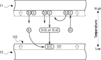
図1に示すように、加熱工程S2では、原基板11が低温側に設置されることで、原基板11(裏面114)における成長層111の形成と、原料体12(主面123)のエッチングと、が同時に行われる。As shown in Figure 1, in the heating process S2, the
加熱工程S2は、原基板11及び原料体12を準閉鎖空間内で加熱する。
The heating process S2 involves heating the
図2に示すように、原基板11及び原料体12において、以下の1)~5)の反応に基づく原料輸送が持続的に行われ、例として原料体12上に成長層121が形成される、と把握することができる。これは、原基板11上に成長層111を形成する場合でも同様である。
なお、本発明の一実施形態に係る原基板11及び原料体12は密着されるが、その場合でも、原基板11及び原料体12間の微小な空隙が原料輸送空間となる、と把握することができる。
2, it can be understood that raw material transport based on the following reactions 1) to 5) is continuously performed in the
In addition, although the
1) SiC(s)→Si(v)+C(s)
2) 2C(s)+Si(v)→SiC2(v)
3) C(s)+2Si(v)→Si2C(v)
4) Si(v)+SiC2(v)→2SiC(s)
5) Si2C(v)→Si(v)+SiC(s)
1) SiC(s) → Si(v)+C(s)
2) 2C(s)+Si(v)→ SiC2 (v)
3) C(s)+2Si(v)→Si 2 C(v)
4) Si(v)+SiC 2 (v)→2SiC(s)
5) Si 2 C (v) → Si (v) + SiC (s)
1)の説明:原基板11の裏面114が熱分解されることで、裏面114からSi原子(Si(v))が脱離する。
2)及び3)の説明:Si原子(Si(v))が脱離することで裏面114に残存したC原子(C(s))は、原料輸送空間内のSi蒸気(Si(v))と反応しSi2C又はSiC2等となって原料輸送空間内に昇華する。
4)及び5)の説明:昇華したSi2C又はSiC2等が、温度勾配によって原料体12の主面123のテラスに到達・拡散し、ステップに到達することで主面123の多形を引き継いで成長層121が成長・形成される(ステップフロー成長)。
Explanation of 1): When the
Explanation of 2) and 3): When Si atoms (Si(v)) are desorbed, the C atoms (C(s)) remaining on the
Explanation of 4) and 5): Sublimated Si2C or SiC2 , etc., reach and diffuse to the terraces of the
加熱工程S2は、原基板11または原料体12表面からSi原子を熱昇華させるSi原子昇華工程S21と、原基板11または原料体12表面に残存したC原子を原料輸送空間内のSi原子と結合させることで昇華させるC原子昇華工程S22と、を含む。
また、加熱工程S2は、原基板11または原料体12表面を、Si原子昇華工程S21及びC原子昇華工程S22に基づきエッチングするエッチング工程S23を含む。加熱工程S2は、例として、原料体12表面がエッチングされる一方、原基板11表面において、上述のステップフロー成長に基づき成長層111を形成する成長工程S24を含む。加熱工程S2に含まれる各工程は逐次、行われる。なお、成長工程S24は、輸送されたSi2C又はSiC2等が過飽和となり凝結することで成長層111を形成するため、PVT(物理気相輸送)に基づく工程である、と把握することができる。
また、加熱工程S2は、SiC単結晶基板表面上のMSBを分解するバンチング分解工程を含む、と把握することができる。
The heating step S2 includes a Si atom sublimation step S21 in which Si atoms are thermally sublimated from the surface of the
The heating step S2 also includes an etching step S23 in which the surface of the
Moreover, the heating step S2 can be understood to include a bunching decomposition step of decomposing the MSBs on the surface of the SiC single crystal substrate.
加熱工程S2における原料輸送の駆動力は、形成された温度勾配に起因する原基板11及び原料体12間の蒸気圧差である、と把握することができる。よって、原基板11及び原料体12のそれぞれの表面における温度差のみならず、原基板11及び原料体12間の結晶構造に起因する蒸気圧差や化学ポテンシャル差も原料輸送の駆動力となり得る、と把握することができる。It can be understood that the driving force for the transport of the raw material in the heating step S2 is the vapor pressure difference between the
なお、加熱工程S2は、原基板11、原料体12、原料輸送防止体28、原基板11及び原料体12がこの順で積み重ねられていた場合、原基板11の主面又は裏面においてのみ成長層111を形成する、と把握することができる。
It can be understood that the heating process S2 forms a
加熱工程S2において準閉鎖空間を形成する装置の一部としてのSiC材料は適宜、原料体12となり得る。
The SiC material as part of the apparatus forming the quasi-closed space in the heating process S2 can be the
加熱工程S2における原料輸送は、ドーパントガス供給手段により準閉鎖空間内にドーパントガスが供給されることで、成長層111のドーピング濃度を調整することができる。ドーパントガス供給手段により準閉鎖空間内にドーパントガスが供給されない場合、成長層111は準閉鎖空間内のドーピング濃度を引き継ぐ、と把握することができる。In the heating step S2, the raw material is transported by supplying a dopant gas into the semi-closed space by a dopant gas supply means, thereby adjusting the doping concentration of the
加熱工程S2における原料輸送は、好ましくは、Si元素を含む気相種及びC元素を含む気相種を有する環境下で行われ、より好ましくは、SiC-Si平衡蒸気圧環境下で行われ、より好ましくは、SiC-C平衡蒸気圧環境下で行われる。The raw material transport in heating step S2 is preferably carried out in an environment having a gas phase species containing Si element and a gas phase species containing C element, more preferably in a SiC-Si equilibrium vapor pressure environment, more preferably in a SiC-C equilibrium vapor pressure environment.
本明細書中の説明における「SiC-Si蒸気圧環境」とは、SiC(固体)とSi(液相)とが気相を介して相平衡状態となっているときの蒸気圧の環境のことを指す。
また、本明細書中の説明における「SiC-C平衡蒸気圧環境」とは、SiC(固相)とC(固相)とが気相を介して相平衡状態となっているときの蒸気圧の環境のことを指す。
In the description of this specification, the term "SiC-Si vapor pressure environment" refers to a vapor pressure environment in which SiC (solid) and Si (liquid phase) are in phase equilibrium via the gas phase.
In addition, the term "SiC-C equilibrium vapor pressure environment" in the description of this specification refers to a vapor pressure environment when SiC (solid phase) and C (solid phase) are in phase equilibrium via the gas phase.
SiC-Si平衡蒸気圧環境は、原子数比Si/Cが1を超える準閉鎖空間が加熱されることで形成される。
SiC-C平衡蒸気圧環境は、原子数比Si/Cが1以下である準閉鎖空間が加熱されることで形成される。
The SiC-Si equilibrium vapor pressure environment is formed by heating a semi-closed space in which the atomic ratio Si/C exceeds 1.
The SiC--C equilibrium vapor pressure environment is formed by heating a semi-closed space in which the atomic ratio Si/C is 1 or less.
加熱工程S2における加熱温度は、好ましくは、1400~2300℃の範囲で設定され、より好ましくは、1600~2000℃の範囲で設定される。The heating temperature in heating step S2 is preferably set in the range of 1400 to 2300°C, more preferably in the range of 1600 to 2000°C.
加熱工程S2における加熱時間は、所望のエッチング量となるよう任意の時間に設定することができる。
例えば、エッチング速度が1.0μm/minの際に、エッチング量を1.0μmとしたい場合には、加熱時間は1min(1分間)となる。
The heating time in the heating step S2 can be set to any time so as to obtain a desired etching amount.
For example, when the etching rate is 1.0 μm/min, in order to set the etching amount to 1.0 μm, the heating time is 1 min (1 minute).
加熱工程S2における温度勾配は、例として、0.1~5.0℃/mmの範囲で設定され、原料輸送空間において一様であることが望ましい。The temperature gradient in the heating process S2 is set, for example, in the range of 0.1 to 5.0°C/mm, and it is desirable that it be uniform in the raw material transport space.
加熱工程S2におけるエッチング量及び成長量は、例として、0.1~20μmの範囲であるが、必要に応じて適宜、変更される。また、エッチング量及び成長量は同等である、と把握することができる。The etching amount and growth amount in the heating step S2 are, for example, in the range of 0.1 to 20 μm, but can be changed as necessary. It can also be understood that the etching amount and growth amount are equivalent.
加熱工程S2におけるエッチング速度及び成長層111の成長速度は、上記温度領域によって制御することができ、例として、0.001~2.0μm/minの範囲で設定できる。The etching rate in the heating process S2 and the growth rate of the
加熱工程S2においてエッチングされるSiC単結晶基板上の表面層は、例として、機械的な加工(例えば、スライスや研削・研磨)やレーザ加工等を経て導入された、傷や潜傷、歪み等のダメージ層300等である、と把握することができる。The surface layer on the SiC single crystal substrate that is etched in the heating process S2 can be understood to be, for example, a
〈分離工程S3〉
分離工程S3における基板13を分離する手法としては、複数本のワイヤを往復運動させることで切断するマルチワイヤソー切断や、プラズマ放電を断続的に発生させて切断する放電加工法、結晶中にレーザ光を照射・集光させて切断の基点となる層を形成するレーザ光を用いて切断する手法等を例示できる。分離工程S3は、レーザ光を用いて切断する手法を採用する場合、基板13の分離における材料のロスを少なくすることができる。
<Separation step S3>
Examples of the method for separating the
分離工程S3は、成長層111を有する原基板11の一部を分離し、成長層111を有する基板13を得る。
また、分離工程S3は、原基板11にダメージ層300を導入する導入工程S31と、ダメージ層300を起点として基板13を剥離する剥離工程S32と、を少なくとも含む。
In the separation step S3, a part of the
The separation step S3 includes at least an introduction step S31 of introducing a damaged
図3に示すように、導入工程S31は、原基板11に対して透過性を有する波長のレーザ光の集光点を、上面から分離すべき基板13の厚みに相当する深さとして、原基板11の内部に位置付け、原基板11にレーザ光を照射してダメージ層300を形成する。As shown in Figure 3, the introduction process S31 positions the focal point of laser light having a wavelength that is transparent to the
図3に示すように、剥離工程S32は、ダメージ層300に沿って原基板11から成長層111を有する基板13を剥離する。剥離工程S32は、原基板11の表面と裏面を台座等に吸着させて分離する手法を例示できる。また、剥離工程S32は、ダメージ層300に沿って細いワイヤを往復運動させる、又は、超音波振動を発生させる等することで原基板11に慣用の機械振動を付与し、ダメージ層300を起点に原基板11から基板13を剥離する。3, in the peeling process S32, the
導入工程S31及び剥離工程S32は、例えば、特開2013-49161号公報、特開2018-207034号公報、特表2017-500725号公報、特開2017-526161号公報等に記載の方法等の公知技術の少なくとも一部を適宜、採用することができる。
また、導入工程S31及び剥離工程S32は、例えば、特表2017-526161号公報、特表2017-500725号公報、特開2018-152582号公報、特表2019-500220号公報、及び、特表2019-511122号公報等の特許文献に記載の方法等の公知技術の少なくとも一部を適宜、採用することができる。
The introduction step S31 and the peeling step S32 can appropriately employ at least a part of known techniques such as those described in, for example, JP 2013-49161 A, JP 2018-207034 A, JP 2017-500725 A, and JP 2017-526161 A.
In addition, the introduction step S31 and the peeling step S32 may appropriately employ at least a part of known techniques such as those described in patent documents such as JP-T-2017-526161, JP-T-2017-500725, JP-A-2018-152582, JP-T-2019-500220, and JP-T-2019-511122.
上記のように、原基板11が設置工程S1、加熱工程S2及び分離工程S3を経ることで、成長層111を有する基板13は製造される。当該工程群が繰り返し行われることで、成長層111を有する基板13は、繰り返し製造され得る。また、製造された成長層111を有する基板13を、原基板11として、再度、当該工程群が行われ得る。As described above, the
設置工程S1、加熱工程S2及び分離工程S3を経て得られた原基板11及び基板13のそれぞれは、残存するダメージ層300を有する。そのため、本発明の一実施形態では、分離工程S3後の原基板11及び基板13に対してエッチング工程S23を含む加熱工程S2を施すことで、原基板11及び基板13において残存するダメージ層300を除去するような構成としてもよい。Each of the
本発明の一実施形態は、設置工程S1、加熱工程S2、設置工程S1a、加熱工程S2a及び分離工程S3をこの順で行ってよい。このとき、設置工程S1aは、原基板11及び原料体12の厚さ方向に沿って、設置工程S1により設置された原基板11及び原料体12の設置順序を逆転させるよう、原基板11及び原料体12を設置する。また、このとき、加熱工程S2aは、加熱工程S2と同様に、原基板11及び原料体12を加熱する。In one embodiment of the present invention, the installation step S1, the heating step S2, the installation step S1a, the heating step S2a, and the separation step S3 may be performed in this order. At this time, the installation step S1a installs the
また、本発明の一実施形態は、設置工程S1、加熱工程S2、加熱工程S2a及び分離工程S3をこの順で行ってよい。このとき、加熱工程S2bは、原基板11及び原料体12の厚さ方向に沿って形成された温度勾配を逆転させるよう、原基板11及び原料体12を加熱する。また、このとき、加熱工程S2bは、加熱工程S2と同様の温度条件、雰囲気下、原料輸送機構に基づき、原基板11及び原料体12を加熱する。In one embodiment of the present invention, the setting step S1, the heating step S2, the heating step S2a, and the separation step S3 may be performed in this order. At this time, the heating step S2b heats the
《半導体基板の製造装置》
以下、本明細書は、本発明の一実施形態である半導体基板の製造装置(以下、単に製造装置という。)について、詳細に説明する。なお、先の製造方法に示した構成と基本的に同一の構成要素については、同一の符号を付してその説明を簡略化する。
Semiconductor substrate manufacturing equipment
Hereinafter, this specification will explain in detail a semiconductor substrate manufacturing apparatus (hereinafter, simply referred to as a manufacturing apparatus) according to one embodiment of the present invention. Note that components that are basically the same as those in the configuration shown in the previous manufacturing method will be assigned the same reference numerals and their explanations will be simplified.
図4に示すように、製造装置は、本体容器20、加熱炉30、高融点容器40、及び、分離手段50を有する。As shown in Figure 4, the manufacturing apparatus has a
原基板11及び原料体12は、原基板11及び原料体12が所定の離間距離1112をなすよう交互に設置される、と把握することができる。It can be understood that the
離間距離1112は、好ましくは10mm以下、より好ましくは7.0mm以下、より好ましくは5.0mm以下、より好ましくは4.0mm以下、より好ましくは3.0mm以下、より好ましくは2.0mm以下、より好ましくは1.7mm以下、より好ましくは1.5mm以下、より好ましくは1.2mm以下、より好ましくは1.0mm以下、より好ましくは700μm以下、より好ましくは500μm以下、より好ましくは200μm以下、より好ましくは100μm以下、より好ましくは70μm以下、より好ましくは50μm以下、より好ましくは20μm以下、より好ましくは10μm以下、より好ましくは、7.0μm以下、より好ましくは5.0μm以下、より好ましくは2.0μm以下、より好ましくは1.0μm以下、より好ましくは0.7μm以下、より好ましくは0.5μm以下、より好ましくは0.2μm以下である。The separation distance 1112 is preferably 10 mm or less, more preferably 7.0 mm or less, more preferably 5.0 mm or less, more preferably 4.0 mm or less, more preferably 3.0 mm or less, more preferably 2.0 mm or less, more preferably 1.7 mm or less, more preferably 1.5 mm or less, more preferably 1.2 mm or less, more preferably 1.0 mm or less, more preferably 700 μm or less, more preferably 500 μm or less, more preferably 200 μm or less, more preferably 100 μm or less, more preferably 70 μm or less, more preferably 50 μm or less, more preferably 20 μm or less, more preferably 10 μm or less, more preferably 7.0 μm or less, more preferably 5.0 μm or less, more preferably 2.0 μm or less, more preferably 1.0 μm or less, more preferably 0.7 μm or less, more preferably 0.5 μm or less, more preferably 0.2 μm or less.
また、離間距離1112は、好ましくは0.1μm以上、より好ましくは0.2μm以上、より好ましくは0.5μm以上、より好ましくは0.7μm以上、より好ましくは1.0μm以上、より好ましくは2.0μm以上、より好ましくは5.0μm以上、より好ましくは7.0μm以上、より好ましくは10μm以上、より好ましくは20μm以上、より好ましくは50μm以上、より好ましくは70μm以上、より好ましくは100μm以上、より好ましくは200μm以上、より好ましくは500μm以上、より好ましくは700μm以上、より好ましくは1.0mm以上、より好ましくは1.2mm以上、より好ましくは1.5mm以上、より好ましくは1.7mm以上、より好ましくは2.0mm以上、より好ましくは3.0mm以上、より好ましくは4.0mm以上、より好ましくは5.0mm以上、より好ましくは7.0mm以上である。 In addition, the separation distance 1112 is preferably 0.1 μm or more, more preferably 0.2 μm or more, more preferably 0.5 μm or more, more preferably 0.7 μm or more, more preferably 1.0 μm or more, more preferably 2.0 μm or more, more preferably 5.0 μm or more, more preferably 7.0 μm or more, more preferably 10 μm or more, more preferably 20 μm or more, more preferably 50 μm or more, more preferably 70 μm or more, more preferably 100 μm or more, more preferably 200 μm or more, more preferably 500 μm or more, more preferably 700 μm or more, more preferably 1.0 mm or more, more preferably 1.2 mm or more, more preferably 1.5 mm or more, more preferably 1.7 mm or more, more preferably 2.0 mm or more, more preferably 3.0 mm or more, more preferably 4.0 mm or more, more preferably 5.0 mm or more, and more preferably 7.0 mm or more.
本体容器20は、離間距離1112を調整するスペーサー等の慣用の距離調整手段27を備えてよい。距離調整手段27は、原基板11及び原料体12と同様の原子種で構成される。The
〈本体容器20〉
図5に示すように、本体容器20は、原基板11及び原料体12を交互に設置可能な容器である。このとき、原基板11及び原料体12は密着するよう設置される。このとき、本体容器20は、準閉鎖空間を内部に有する。また、本体容器20は、加熱された際に原基板11を構成する原子種を含む気相種の蒸気圧を内部に発生させる。このとき、本体容器20により設置される原基板11及び原料体12のそれぞれの数量に制限はない。なお、原基板11及び原料体12は、原基板11、原料体12及び原基板11の順で交互に設置されてよく、原料体12、原基板11及び原料体12の順で交互に設置されてよい。
<
As shown in FIG. 5, the
図6に示すように、本体容器20は、原基板11及び原料体12を交互に設置可能な容器である。このとき、原基板11及び原料体12は距離調整手段27により離間距離1112、離間するよう交互に設置される。なお、原基板11及び原料体12は、原基板11、原料体12及び原基板11の順で交互に設置されてよく、原料体12、原基板11及び原料体12の順で交互に設置されてよい。
また、本体容器20は、準閉鎖空間を内部に有する。このとき、本体容器20は、加熱された際に原基板11を構成する原子種を含む気相種の蒸気圧を内部に発生させる。このとき、本体容器20により設置される原基板11及び原料体12のそれぞれの数量に制限はない。
6,
Furthermore,
図7に示すように、本体容器20は、原基板11及び原料体12を含む単位処理体1X間に、異なる単位処理体1X間の、原基板11及び原料体12間の原料輸送を防止する原料輸送防止体28を設置可能な容器である。このとき、本体容器20により設置される単位処理体1X及び原料輸送防止体28のそれぞれの数量に制限はない。なお、原基板11及び原料体12は、原基板11、原料体12及び原基板11の順で交互に設置されてよく、原料体12、原基板11及び原料体12の順で交互に設置されてよい。
原料輸送防止体28は、好ましくは、上述の原基板11及び原料体12間の原料輸送における輸送先又は輸送元とならないような、W,Re,Os,Ta,Mo等の高融点金属や、Ta9C8,HfC,TaC,NbC,ZrC,Ta2C,TiC,WC,MoC等の炭化物や、HfB2,TaB2,ZrB2,NB2,TiB2等のホウ化物等である。
7, the
The raw material
図8に示すように、複数の本体容器20のそれぞれは、1の原基板11を収容する。このとき、複数の本体容器20のそれぞれは、互いに嵌合可能である。このとき、本体容器20は、準閉鎖空間を内部に有する。このとき、本体容器20は、加熱された際に原基板11を構成する原子種を含む気相種の蒸気圧を内部に発生させる。このとき、1の原基板11を収容する本体容器20の数量に制限はない。なお、複数の本体容器20のそれぞれは、原基板11及び原料体12を収容する構成としてもよい。As shown in FIG. 8, each of the multiple
本体容器20は、例として、SiC多結晶を含むSiC材料で構成されている。よって、本体容器20の少なくとも一部は、原料体12として、原料輸送における輸送先又は輸送元となり得る。The
本発明の一実施形態では、図5~図8のそれぞれにおける構成の少なくとも一部を適宜組み合わせることで、少なくとも原基板11及び原料体12を交互に設置可能な本体容器を実現してよい。In one embodiment of the present invention, a main container in which at least the
加熱された本体容器20内の環境は、例として、Si元素を含む気相種及びC元素を含む気相種の混合系の蒸気圧環境となることが望ましい。このSi元素を含む気相種としては、Si、Si2、Si3、Si2C、SiC2、SiC等を例示することができる。また、C元素を含む気相種としては、Si2C、SiC2、SiC、C等を例示することができる。
The environment inside the heated
本体容器20のドーパント及びドーピング濃度は、形成したい成長層111又は121のドーパント及びドーピング濃度に合わせて選択することができる。ドーパントとしては、N元素を例示することができる。The dopant and doping concentration of the
また、本体容器20の加熱処理時に、内部空間にSi元素を含む気相種及びC元素を含む気相種の蒸気圧を発生させる構成であれば、その構造を採用することができる。例として、内面の一部にSiC多結晶が露出した構成や、本体容器20内に別途、SiC多結晶を設置する構成等を示すことができる。In addition, any structure can be adopted so long as it generates vapor pressure of gaseous species containing Si and gaseous species containing C in the internal space during the heat treatment of the
本体容器20は、例として、互いに嵌合可能な上容器23及び下容器24を備える嵌合容器である。上容器23と下容器24の嵌合部には、微小な間隙25が形成されており、この間隙25から本体容器20内の排気(真空引き)が可能なよう構成されている。The
〈Si蒸気供給源26〉
本体容器20は、Si蒸気供給源26(図4において図示せず、図5においては図示。
)を有する。Si蒸気供給源26は、本体容器20内の準閉鎖空間の原子数比Si/Cを、1を超えるよう調整する目的で用いられる。Si蒸気供給源としては、固体のSi(Si片やSi粉末等のSiペレット)やSi化合物を例示することができる。
<Si
The
The Si
例えば、本発明の一実施形態のように、本体容器20の全体がSiC多結晶で構成されている場合には、Si蒸気供給源26を設置することで、本体容器20内の原子数比Si/Cが1を超える。具体的には、化学量論比1:1を満たすSiC多結晶の本体容器20内に、化学量論比1:1を満たす原基板11及び原料体12と、Si蒸気供給源26と、を設置した場合には、本体容器20内の原子数比Si/Cは1を超えることとなる。For example, in the case where the entire
本発明の一実施形態に係るSiC-Si平衡蒸気圧環境は、原子数比Si/Cが1を超える準閉鎖空間が加熱されることで形成される。また、本発明の一実施形態に係るSiC-C平衡蒸気圧環境は、原子数比Si/Cが1以下である準閉鎖空間が加熱されることで形成される。本発明の一実施形態に係る本体容器20は、それぞれ、SiC-Si平衡蒸気圧環境又はSiC-C平衡蒸気圧環境となるよう適宜、所定の部材を収容する構成としてよい。The SiC-Si equilibrium vapor pressure environment according to one embodiment of the present invention is formed by heating a quasi-closed space in which the atomic ratio Si/C exceeds 1. The SiC-C equilibrium vapor pressure environment according to one embodiment of the present invention is formed by heating a quasi-closed space in which the atomic ratio Si/C is 1 or less. The
〈加熱炉30〉
加熱炉30は、本体容器20の上容器23から下容器24に向かって温度が下がる/上がるよう温度勾配を形成するよう加熱する構成となっている。これにより、原基板11の厚み方向に温度勾配が形成される。
<
The
加熱炉30は、図4に示すように、被処理物(原基板11や本体容器20、高融点容器40等)を1000℃以上2300℃以下の温度に加熱することが可能な本加熱室31と、被処理物を500℃以上の温度に予備加熱可能な予備室32と、本体容器20を収容可能な高融点容器40と、この高融点容器40を予備室32から本加熱室31へ移動可能な移動手段33(移動台)と、を備えている。As shown in FIG. 4, the
本加熱室31は、平面断面視で正六角形に形成されており、その内側に高融点容器40が設置される。本加熱室31内は、加熱ヒータ34(メッシュヒータ)が備えられている。また、本加熱室31の側壁や天井には多層熱反射金属板が固定されている(図示せず。)。多層熱反射金属板は、加熱ヒータ34の熱を本加熱室31の略中央部に向け反射させるように構成されている。The
加熱ヒータ34は、本加熱室31内において、被処理物が収容される高融点容器40を取り囲むように設置される。このとき、加熱ヒータ34の外側に多層熱反射金属板が設置されることで、1000℃以上2300℃以下の温度範囲における昇温が可能となる。The
加熱ヒータ34は、例として、抵抗加熱式のヒータや高周波誘導加熱式のヒータを採用することができる。
The
加熱ヒータ34は、高融点容器40内に温度勾配を形成可能な構成を採用してもよい。
加熱ヒータ34は、例として、上側(若しくは下側)に多くのヒータが設置されるよう構成してもよい。また、加熱ヒータ34は、上側(若しくは下側)に向かうにつれて幅が大きくなるように構成してもよい。あるいは、加熱ヒータ34は、上側(若しくは下側)に向かうにつれて供給される電力を大きくすることが可能なよう構成してもよい。また、加熱ヒータ34は、温度勾配の形成方向を反転可能であってよい。
The
For example, the
本加熱室31には、本加熱室31内の排気を行う真空形成用バルブ35と、本加熱室31内に不活性ガスを導入する不活性ガス注入用バルブ36と、本加熱室31内の真空度を測定する真空計37と、が接続されている。
Connected to the
真空形成用バルブ35は、本加熱室31内を排気して真空引きする真空引ポンプと接続されている(図示せず。)。この真空形成用バルブ35及び真空引きポンプにより、本加熱室31内の真空度は、好ましくは、10Pa以下、より好ましくは、1.0Pa以下、最も好ましくは、10-3Pa以下に調整することができる。この真空引きポンプとしては、ターボ分子ポンプを例示することができる。
The
不活性ガス注入用バルブ36は、不活性ガス供給源と接続されている(図示せず。)。この不活性ガス注入用バルブ36及び不活性ガス供給源により、本加熱室31内に不活性ガスを10-5~104Paの範囲で導入することができる。この不活性ガスとしては、Ar等を選択することができる。
The inert
不活性ガス注入用バルブ36は、本体容器20内にドーパントガスを供給可能なドーパントガス供給手段である。すなわち、不活性ガスにドーパントガス(例として、N2等)を選択することにより、成長層111のドーピング濃度を高めることができる。
The inert
予備室32は、本加熱室31と接続されており、移動手段33により高融点容器40を移動可能に構成されている。なお、本実施形態の予備室32は、本加熱室31の加熱ヒータ34の余熱により昇温可能なよう構成されている。例として、本加熱室31を2000℃まで昇温した場合には、予備室32は1000℃程度まで昇温され、被処理物の脱ガス処理を行うことができる。The
移動手段33は、高融点容器40を載置して、本加熱室31及び予備室32間を移動可能に構成されている。The moving means 33 is configured to be able to carry the high
移動手段33による本加熱室31と予備室32間の搬送は、最短1分程で完了するため、1.0~1000℃/minでの昇温・降温を実現することができる。これにより、急速昇温及び急速降温が行えるため、昇温中及び降温中の低温成長履歴を持たない表面形状を観察することが可能である。また、図4において、予備室32は本加熱室31の下方に設置されているが、予備室32はこれに限られず何れの方向に設置されてもよい。
Transport between the
本実施形態に係る移動手段33は、高融点容器40を載置する移動台である。この移動台と高融点容器40の接触部と、が熱の伝播経路となる。これにより、移動台と高融点容器40の接触部側が低温側となるよう高融点容器40内に温度勾配を形成することができる。The moving means 33 in this embodiment is a moving table on which the high
本実施形態の加熱炉30では、高融点容器40の底部が移動台と接触しているため、高融点容器40の上容器41から下容器42に向かって温度が下がるように温度勾配が設けられる。In the
温度勾配の方向は、移動台と高融点容器40の接触部の位置を変更することで、任意の方向に設定することができる。例として、移動台に吊り下げ式等を採用して、接触部を高融点容器40の天井に設ける場合には、熱が上方向に逃げる。そのため、温度勾配は、高融点容器40の上容器41から下容器42に向かって温度が上がるように温度勾配が設けられることとなる。なお、この温度勾配は、原基板11及び原料体12の厚さ方向に沿って形成されていることが望ましい。また、上記のように、温度勾配は、加熱ヒータ34の構成により形成されてもよい。The direction of the temperature gradient can be set to any direction by changing the position of the contact point between the moving table and the high
〈高融点容器40〉
本実施形態に係る加熱炉30内のSi元素を含む気相種の蒸気圧環境は、高融点容器40及びSi蒸気供給材料44を用いて形成している。例として、本体容器20の周囲にSi元素を含む気相種の蒸気圧の環境を形成可能な方法であれば、本発明の半導体基板の製造装置に採用することができる。
<High
The vapor pressure environment of the gaseous species containing Si element in the
高融点容器40は、好ましくは、本体容器20を構成する材料の融点と同等若しくはそれ以上の融点を有する、高融点材料を含んで構成されている。The high
高融点容器40は、例として、汎用耐熱部材であるC、高融点金属であるW,Re,Os,Ta,Mo、炭化物であるTa9C8,HfC,TaC,NbC,ZrC,Ta2C,TiC,WC,MoC、窒化物であるHfN,TaN,BN,Ta2N,ZrN,TiN、ホウ化物であるHfB2,TaB2,ZrB2,NB2,TiB2、SiC多結晶等を例示することができる。
Examples of high-
図5に示すように、高融点容器40は、本体容器20と同様に、互いに嵌合可能な上容器41と、下容器42と、を備える嵌合容器であり、本体容器20を収容可能に構成されている。上容器41と下容器42の嵌合部には、微小な間隙43が形成されており、この間隙43から高融点容器40内の排気(真空引き)が可能なよう構成されている。5, the high
高融点容器40は、高融点容器40内にSi元素を含む気相種の蒸気圧を供給可能なSi蒸気供給材料44を有している。The high
〈Si蒸気供給材料44〉
Si蒸気供給材料44は、加熱処理時にSi蒸気を高融点容器40内に発生させる構成であればよく、例として、固体のSi(Si片やSi粉末等のSiペレット)やSi化合物を例示することができる。
<Si
The Si
Si蒸気供給材料44は、例として、高融点容器40の内壁を被覆する薄膜である。The Si
高融点容器40がTaC等の金属化合物である場合、Si蒸気供給材料44は、例として、高融点容器40を構成する金属原子及びSi原子のシリサイド材料である。When the high
〈分離手段〉
分離手段50は、成長層111を有する原基板11の一部を分離し、成長層111を有する基板13を得る。
また、分離手段50は、原基板11にダメージ層300を導入する導入手段51と、ダメージ層300を起点として基板13を剥離する剥離手段52と、を少なくとも含む。
<Separation means>
The separating means 50 separates a part of the
The separating means 50 includes at least an introducing means 51 for introducing a damaged
図3に示すように、導入手段51は、成長層111及び原基板11に対して透過性を有する波長のレーザ光の集光点を、上面から分離すべき基板13の厚みに相当する深さとして、原基板11の内部に位置付け、原基板11にレーザ光を照射してダメージ層300を形成する。As shown in Figure 3, the introduction means 51 positions the focal point of laser light having a wavelength that is transparent to the
導入手段51は、例えば、吸着チャック等の慣用の手法に基づき原基板11及び原料体12を保持可能な保持手段(図示せず。)と、パルス発振するレーザ光を照射可能な光源である発振手段511と、当該レーザ光を集光可能なレンズ等の慣用の集光手段512と、を備え、発振手段511及び集光手段512の少なくとも一部を走査可能である。
また、導入手段51は、導入手段51を構成する各装置の少なくとも一部は、任意の軸方向においてアラインメント可能な慣用の調整手段を有する。なお、当該レーザ光の波長、時間幅、出力及びスポット径等に制限はない。
The introduction means 51 includes, for example, a holding means (not shown) capable of holding the
At least a part of each device constituting the introduction means 51 has a conventional adjustment means capable of alignment in any axial direction. There is no limitation on the wavelength, time width, output, spot diameter, etc. of the laser light.
図3に示すように、剥離手段52は、ダメージ層300に沿って原基板11から成長層111を有する基板13を剥離する。
また、剥離手段52は、原基板11の表面と裏面を台座等に吸着させて分離する手法を例示できる。
また、剥離手段52は、ダメージ層300に沿って細いワイヤを往復運動させる、又は、超音波振動を発生させる等することで原基板11に慣用の機械振動を付与し、ダメージ層300を起点に原基板11から基板13を剥離する。
As shown in FIG. 3, the peeling means 52 peels off the
The peeling means 52 may be, for example, a method of adsorbing the front and back surfaces of the
In addition, the peeling means 52 applies conventional mechanical vibrations to the
剥離手段52は、原基板11を収容可能な剥離用高融点容器と、吸着チャック等の慣用の手法に基づき原基板11を保持可能な保持手段と、を有する。
また、剥離手段52は、超音波振動を含む慣用の機械振動を発生可能であり当該機械振動を原基板11に与える振動手段と、純水等の液体を供給可能であり慣用の手法に基づく液体供給手段と、を有する。
The peeling means 52 has a high melting point container for peeling capable of accommodating the
The peeling means 52 also has vibration means capable of generating conventional mechanical vibrations including ultrasonic vibrations and applying the mechanical vibrations to the
導入手段51及び剥離手段52は、公知の技術を実現するための装置等を適宜、採用することができる。
導入手段51及び剥離手段52のそれぞれは、例えば、特開2013-49161号公報、特開2018-207034号公報、特表2017-500725号公報、特開2017-526161号公報等に記載の装置等の少なくとも一部を適宜、採用することができる。
また、導入手段51及び剥離手段52のそれぞれは、例えば、特表2017-526161号公報、特表2017-500725号公報、特開2018-152582号公報、特表2019-500220号公報、及び、特表2019-511122号公報等の特許文献に記載の装置等の少なくとも一部を適宜、採用することができる。
The introduction means 51 and the peeling means 52 can be appropriately made of devices and the like for realizing known techniques.
Each of the introduction means 51 and the peeling means 52 can appropriately adopt at least a part of the devices described in, for example, JP 2013-49161 A, JP 2018-207034 A, JP 2017-500725 A, JP 2017-526161 A, etc.
In addition, each of the introduction means 51 and the peeling means 52 can appropriately adopt at least a portion of the devices described in patent documents such as, for example, JP-T-2017-526161, JP-T-2017-500725, JP-A-2018-152582, JP-T-2019-500220, and JP-T-2019-511122.
上記のように、原基板11が本体容器20、加熱炉30及び分離手段50による処理を経ることで、成長層111を有する基板13は製造される。当該処理が繰り返し行われることで、成長層111を有する基板13が繰り返し製造されてよい。また、当該処理は、成長層111を有する基板13を新たな原基板11として、行われてもよい。As described above, the
本明細書は、参考例1~3を交えて、本発明に係る作用効果を説明する。
《参考例1》
以下の条件で、SiC単結晶基板E10は本体容器20に収容され、本体容器20は高融点容器40に収容されている。
This specification will explain the effects of the present invention with reference to Reference Examples 1 to 3.
《Reference example 1》
Under the following conditions, the SiC single crystal substrate E10 is housed in the
〈SiC単結晶基板E10〉
多型:4H-SiC
基板サイズ:横幅(10mm)、縦幅(10mm)、厚み(0.3mm)
オフ方向及びオフ角:<11-20>方向4°オフ
成長面:(0001)面
MSBの有無:無し
ダメージ層:無し
<SiC single crystal substrate E10>
Polymorphism: 4H-SiC
Board size: width (10 mm), length (10 mm), thickness (0.3 mm)
Off-direction and off-angle: 4° off in the <11-20> direction Growth surface: (0001) surface Presence or absence of MSB: None Damaged layer: None
〈本体容器〉
材料:SiC多結晶
容器サイズ:直径(60mm)、高さ(4.0mm)
SiC単結晶基板E10とSiC材料との距離:2.0mm
容器内の原子数比Si/C:1以下
<Main container>
Material: SiC polycrystalline Container size: diameter (60 mm), height (4.0 mm)
Distance between SiC single crystal substrate E10 and SiC material: 2.0 mm
Atomic ratio Si/C in the container: 1 or less
〈高融点容器〉
材料:TaC
容器サイズ:直径(160mm)、高さ(60mm)
Si蒸気供給材料44(Si化合物):TaSi2
<High melting point container>
Material: TaC
Container size: diameter (160 mm), height (60 mm)
Si vapor supply material 44 (Si compound): TaSi 2
上記条件で設置したSiC単結晶基板E10は、以下の条件で加熱処理されている。
加熱温度:1700℃
加熱時間:300min
温度勾配:1.0℃/mm
成長速度:5.0nm/min
本加熱室31の真空度:10-5Pa
The SiC single crystal substrate E10 placed under the above conditions was heat-treated under the following conditions.
Heating temperature: 1700℃
Heating time: 300min
Temperature gradient: 1.0°C/mm
Growth rate: 5.0nm/min
Degree of vacuum in the main heating chamber 31: 10 −5 Pa
図9は、成長層E11において、BPDから他の欠陥・転位(TED等)に変換した変換率を求める手法の説明図である。 Figure 9 is an explanatory diagram of a method for determining the conversion rate of BPDs to other defects/dislocations (TEDs, etc.) in the growth layer E11.
図9(a)は、加熱工程により成長層E11を成長させた様子を示している。この加熱工程では、SiC単結晶基板E10に存在していたBPDが、ある確率でTEDに変換される。そのため、成長層E11の表面には、100%変換されない限り、TEDとBPDが混在していることとなる。 Figure 9 (a) shows the state in which the growth layer E11 is grown by a heating process. In this heating process, the BPDs present in the SiC single crystal substrate E10 are converted to TEDs with a certain probability. Therefore, unless 100% conversion is achieved, TEDs and BPDs will be present on the surface of the growth layer E11.
図9(b)は、KOH溶解エッチング法を用いて成長層E11中の欠陥を確認した様子を示している。このKOH溶解エッチング法は、約500℃に加熱した溶解塩(KOH等)にSiC単結晶基板E10を浸し、転位や欠陥部分にエッチピットを形成し、そのエッチピットの大きさ・形状により転位の種類を判別する手法である。この手法により、成長層E11表面に存在しているBPD数は評価される。 Figure 9 (b) shows the state where defects in the growth layer E11 were confirmed using the KOH dissolution etching method. This KOH dissolution etching method is a technique in which the SiC single crystal substrate E10 is immersed in molten salt (such as KOH) heated to approximately 500°C, etch pits are formed in the dislocations and defects, and the type of dislocation is identified based on the size and shape of the etch pits. This method allows the number of BPDs present on the surface of the growth layer E11 to be evaluated.
図9(c)は、KOH溶解エッチング後に成長層E11を除去する様子を示している。
本手法では、エッチピット深さまで機械研磨やCMP等により平坦化した後、熱エッチングにより成長層E11を除去することで、SiC単結晶基板E10の表面は表出している。
FIG. 9C shows the state in which the growth layer E11 is removed after KOH dissolution etching.
In this method, the surface of the SiC single crystal substrate E10 is exposed by planarizing the surface to the depth of the etch pits by mechanical polishing, CMP, or the like, and then removing the growth layer E11 by thermal etching.
図9(d)は、成長層E11を除去したSiC単結晶基板E10に対し、KOH溶解エッチング法を用いてSiC単結晶基板E10中の欠陥を確認した様子を示している。この手法により、SiC単結晶基板E10表面に存在しているBPD数は評価される。 Figure 9(d) shows the state in which defects in the SiC single crystal substrate E10 from which the growth layer E11 has been removed are confirmed using a KOH dissolution etching method. By this method, the number of BPDs present on the surface of the SiC single crystal substrate E10 is evaluated.
図9に示した一連の順序により、成長層E11表面に存在するBPDの数(図9(b)参照)と、SiC単結晶基板E10表面に存在するBPDの数(図9(d))と、を比較することで、加熱工程S2中にBPDから他の欠陥・転位に変換したBPD変換率を得ることができる。 By comparing the number of BPDs present on the surface of the growth layer E11 (see Figure 9(b)) with the number of BPDs present on the surface of the SiC single crystal substrate E10 (see Figure 9(d)) using the sequence shown in Figure 9, the BPD conversion rate of BPDs converted to other defects/dislocations during the heating process S2 can be obtained.
参考例1の成長層E11表面に存在するBPDの数は約0/cm-2であり、SiC単結晶基板E10表面に存在するBPDの数は1000個cm-2であった。すなわち、表面にMSBが存在しないSiC単結晶基板E10を原子数比Si/Cが1以下である準閉鎖空間に設置し加熱することによりBPDが低減・除去される、と把握することができる。 The number of BPDs present on the surface of growth layer E11 in Reference Example 1 was approximately 0/cm -2 , and the number of BPDs present on the surface of SiC single crystal substrate E10 was 1000/cm -2 . In other words, it can be understood that BPDs are reduced or removed by placing SiC single crystal substrate E10, the surface of which is free of MSBs, in a semi-closed space in which the atomic ratio Si/C is 1 or less and heating it.
参考例1では、本体容器20内の原子数比Si/Cが1以下となるよう本体容器20内にSiC-C平衡蒸気圧環境が形成されている。上記の方法におけるエッチング工程S23を含む加熱工程S2と、本発明の一実施形態に係るエッチング工程を含む加熱工程S2と、は同一の反応素過程に基づくため、本発明の一実施形態に係るエッチング工程においてもBPDが低減・除去され得る、と把握することができる。In Reference Example 1, a SiC-C equilibrium vapor pressure environment is formed within the
《参考例2》
以下の条件で、SiC単結晶基板E10を本体容器20に収容し、さらに本体容器20を高融点容器40に収容した。
《Reference example 2》
Under the following conditions, the SiC single crystal substrate E10 was housed in the
〈SiC単結晶基板E10〉
多型:4H-SiC
基板サイズ:横幅(10mm)、縦幅(10mm)、厚み(0.3mm)
オフ方向及びオフ角:<11-20>方向4°オフ
成長面:(0001)面
MSBの有無:有り
<SiC single crystal substrate E10>
Polymorphism: 4H-SiC
Board size: width (10 mm), length (10 mm), thickness (0.3 mm)
Off-direction and off-angle: 4° off in the <11-20> direction Growth surface: (0001) surface Presence or absence of MSB: Present
〈本体容器〉
材料:SiC多結晶
容器サイズ:直径(60mm)、高さ(4.0mm)
SiC単結晶基板E10とSiC材料との距離:2.0mm
Si蒸気供給源26:Si片
容器内の原子数比Si/C:1を超える
<Main container>
Material: SiC polycrystalline Container size: diameter (60 mm), height (4.0 mm)
Distance between SiC single crystal substrate E10 and SiC material: 2.0 mm
Si vapor source 26: Si piece Atomic ratio Si/C in the container: exceeds 1
本体容器20内に、SiC単結晶基板と共にSi片を収容することで、容器内の原子数比Si/Cが1を超える。By housing the Si pieces together with the SiC single crystal substrate in the
〈高融点容器〉
材料:TaC
容器サイズ:直径160mm×高さ60mm
Si蒸気供給材料44(Si化合物):TaSi2
<High melting point container>
Material: TaC
Container size: diameter 160mm x height 60mm
Si vapor supply material 44 (Si compound): TaSi 2
上記条件で設置したSiC単結晶基板E10は、以下の条件で加熱処理されている。
加熱温度:1800℃
加熱時間:60min
温度勾配:1.0℃/mm
成長速度:68nm/min
本加熱室31真空度:10-5Pa
The SiC single crystal substrate E10 placed under the above conditions was heat-treated under the following conditions.
Heating temperature: 1800℃
Heating time: 60min
Temperature gradient: 1.0°C/mm
Growth rate: 68nm/min
図10は、成長層E11の成長前のSiC単結晶基板E10表面のSEM像である。図10(a)は倍率×1000で観察したSEM像であり、図10(b)は倍率×100000で観察したSEM像である。この成長層E11の成長前のSiC単結晶基板E10表面には、MSBが形成されており、高さ3.0nm以上のステップが、平均42nmのテラス幅で配列していることが把握することができる。なお、ステップ高さは、AFMにより測定した。 Figure 10 is an SEM image of the surface of SiC single crystal substrate E10 before the growth of growth layer E11. Figure 10(a) is an SEM image observed at a magnification of x1000, and Figure 10(b) is an SEM image observed at a magnification of x100,000. It can be seen that an MSB is formed on the surface of SiC single crystal substrate E10 before the growth of growth layer E11, and steps with a height of 3.0 nm or more are arranged with an average terrace width of 42 nm. The step height was measured by AFM.
図11は、成長層E11の成長後のSiC単結晶基板E10表面のSEM像である。図11(a)は倍率×1000で観察したSEM像であり、図11(b)は倍率×100000で観察したSEM像である。
参考例2の成長層E11表面には、MSBは形成されておらず、1.0nm(フルユニットセル)のステップが、14nmのテラス幅で規則正しく配列していることが把握することができる。なお、ステップ高さは、AFMにより測定した。
11A and 11B are SEM images of the surface of the SiC single crystal substrate E10 after the growth of the growth layer E11. Fig. 11A is an SEM image observed at a magnification of ×1000, and Fig. 11B is an SEM image observed at a magnification of ×100,000.
It can be seen that no MSB is formed on the surface of the growth layer E11 of Reference Example 2, and steps of 1.0 nm (full unit cell) are regularly arranged with a terrace width of 14 nm. The step height was measured by AFM.
そのため、表面にMSBが存在するSiC単結晶基板E10を原子数比Si/Cが1を超える準閉鎖空間に設置し加熱することによりMSBが分解された成長層E11が形成される、と把握することができる。Therefore, it can be understood that by placing a SiC single crystal substrate E10 having MSB on its surface in a quasi-closed space with an atomic ratio Si/C exceeding 1 and heating it, a growth layer E11 in which the MSB is decomposed is formed.
参考例2では、本体容器20内の原子数比Si/Cが1を超えるようSi蒸気供給源26が設置されているため、本体容器20内に、SiC-Si平衡蒸気圧環境が形成されている。
上記の方法におけるエッチング工程S23を含む加熱工程S2と、本発明の一実施形態に係るエッチング工程を含む加熱工程と、は同一の反応素過程に基づくため、本発明の一実施形態に係るエッチング工程においてもSiC単結晶基板表面上のMSBは分解され得る、と把握することができる。
In Reference Example 2, since the Si
Since the heating step S2 including the etching step S23 in the above-described method and the heating step including the etching step according to one embodiment of the present invention are based on the same elementary reaction process, it can be understood that the MSB on the surface of the SiC single crystal substrate can also be decomposed in the etching step according to one embodiment of the present invention.
《参考例3》
図12は、本発明に係るSiC単結晶基板の製造方法にて成長させた加熱温度と成長速度の関係を示すグラフである。このグラフの横軸は温度の逆数であり、このグラフの縦軸は成長速度を対数表示している。SiC単結晶基板E10を原子数比Si/Cが1を超える空間(本体容器20内)に設置して、SiC単結晶基板E10に成長層E11を成長させた結果を〇印で示す。また、SiC単結晶基板E10を原子数比Si/Cが1以下である空間(本体容器20内)に設置して、SiC単結晶基板E10に成長層E11を成長させた結果を×印で示している。
《Reference example 3》
12 is a graph showing the relationship between the heating temperature and the growth rate grown by the method for producing a SiC single crystal substrate according to the present invention. The horizontal axis of this graph is the reciprocal of the temperature, and the vertical axis of this graph is the logarithmic growth rate. The result of placing the SiC single crystal substrate E10 in a space (inside the main body container 20) where the atomic ratio Si/C exceeds 1 and growing the growth layer E11 on the SiC single crystal substrate E10 is shown by a circle. Also, the result of placing the SiC single crystal substrate E10 in a space (inside the main body container 20) where the atomic ratio Si/C is 1 or less and growing the growth layer E11 on the SiC single crystal substrate E10 is shown by a cross.
また、図12のグラフは、SiC-Si平衡蒸気圧環境におけるSiC基板成長の熱力学計算の結果を破線(アレニウスプロット)で示し、SiC-C平衡蒸気圧環境におけるSiC基板成長の熱力学計算の結果を二点鎖線(アレニウスプロット)で示している。 In addition, the graph in Figure 12 shows the results of thermodynamic calculations of SiC substrate growth in a SiC-Si equilibrium vapor pressure environment using a dashed line (Arrhenius plot), and the results of thermodynamic calculations of SiC substrate growth in a SiC-C equilibrium vapor pressure environment using a two-dot chain line (Arrhenius plot).
本手法においては、SiC原料とSiC基板間の蒸気圧環境が、SiC-C平衡蒸気圧環境又はSiC-C平衡蒸気圧環境となる条件下で、化学ポテンシャル差や温度勾配を成長駆動力として、SiC単結晶基板E10を成長させている。この化学ポテンシャル差は、SiC多結晶とSiC単結晶の表面で発生する気相種の分圧差を例示することができる。In this method, under conditions where the vapor pressure environment between the SiC raw material and the SiC substrate is a SiC-C equilibrium vapor pressure environment or a SiC-C equilibrium vapor pressure environment, the SiC single crystal substrate E10 is grown using a chemical potential difference or a temperature gradient as the growth driving force. An example of this chemical potential difference is the partial pressure difference between the gas phase species generated on the surfaces of the SiC polycrystal and the SiC single crystal.
ここで、SiC原料(輸送元)とSiC基板(輸送先)から発生する蒸気の分圧差を成長量とした場合、SiC成長速度は以下の数1で求められる。Here, if the growth amount is the partial pressure difference between the vapor generated from the SiC raw material (source) and the SiC substrate (destination), the SiC growth rate can be calculated using the

ここで、TはSiC原料側の温度、miは気相種(SixCy)の分子量、kはボルツマン定数である。また、P輸送元i-P輸送先iは、原料ガスが過飽和な状態となって、SiCとして析出した成長量であり、原料ガスとしてはSiC,Si2C,SiC2が想定される。 Here, T is the temperature of the SiC source, m i is the molecular weight of the gas phase species (Si x C y ), and k is the Boltzmann constant. Also, P transport source i - P transport destination i is the growth amount of SiC precipitated when the source gas becomes supersaturated, and the source gas is assumed to be SiC, Si 2 C, or SiC 2 .
よって、破線は、SiC(固体)とSi(液相)とが気相を介して相平衡状態となっているときの蒸気圧環境において、SiC多結晶を原料としてSiC単結晶を成長させた際の熱力学計算の結果である。当該結果は、具体的には、数1を用いて以下の条件(i)~(iv)で熱力学計算されて得られたものである。
(i)体積一定のSiC-Si平衡蒸気圧環境であること
(ii)成長駆動力は、本体容器20内の温度勾配と、SiC多結晶とSiC単結晶の蒸気圧差(化学ポテンシャル差)であること
(iii)原料ガスは、SiC,Si2C,SiC2である
(iv)原料がSiC単結晶基板E10のステップに吸着する吸着係数は0.001である
Therefore, the dashed line is the result of a thermodynamic calculation when a SiC single crystal is grown using a SiC polycrystal as a raw material in a vapor pressure environment when SiC (solid) and Si (liquid phase) are in phase equilibrium via the gas phase. Specifically, the result was obtained by performing a thermodynamic
(i) A constant volume SiC-Si equilibrium vapor pressure environment is required. (ii) The growth driving force is the temperature gradient in the
また、二点鎖線は、SiC(固相)とC(固相)とが気相を介して相平衡状態となっているときの蒸気圧環境において、SiC多結晶を原料としてSiC単結晶を成長させた際の熱力学計算の結果である。当該結果は、具体的には、数1を用いて以下の条件(i)~(iv)で熱力学計算されて得られたものである。
(i)体積一定のSiC-C平衡蒸気圧環境である
(ii)成長駆動力は、本体容器20内の温度勾配と、SiC多結晶とSiC単結晶の蒸気圧差(化学ポテンシャル差)である
(iii)原料ガスはSiC,Si2C,SiC2である
(iv)原料がSiC単結晶基板E10のステップに吸着する吸着係数は0.001である
なお、熱力学計算に用いた各化学種のデータはJANAF熱化学表の値を採用した。
The two-dot chain line represents the results of thermodynamic calculations when a SiC single crystal is grown using a SiC polycrystal as a raw material in a vapor pressure environment in which SiC (solid phase) and C (solid phase) are in phase equilibrium via the gas phase. Specifically, the results were obtained by thermodynamic
(i) It is a SiC-C equilibrium vapor pressure environment with a constant volume. (ii) The growth driving force is the temperature gradient inside the
この図12のグラフによれば、SiC単結晶基板E10を原子数比Si/Cが1を超える空間(本体容器20内)に設置して、SiC単結晶基板E10に成長層E11を成長させた結果(〇印)は、SiC-Si平衡蒸気圧環境におけるSiC成長の熱力学計算の結果と傾向が一致している、と把握することができる。また、SiC単結晶基板E10を原子数比Si/Cが1以下である空間(本体容器20内)に設置して、SiC単結晶基板E10に成長層E11を成長させた結果(×印)は、SiC-C平衡蒸気圧環境におけるSiC成長の熱力学計算の結果と傾向が一致している、と把握することができる。12, it can be understood that the results (marked with a circle) of growing a growth layer E11 on a SiC single crystal substrate E10 by placing the SiC single crystal substrate E10 in a space (inside the main container 20) where the atomic ratio Si/C exceeds 1, are consistent with the results of a thermodynamic calculation of SiC growth in a SiC-Si equilibrium vapor pressure environment. It can also be understood that the results (marked with a cross) of growing a growth layer E11 on a SiC single crystal substrate E10 by placing the SiC single crystal substrate E10 in a space (inside the main container 20) where the atomic ratio Si/C is 1 or less, are consistent with the results of a thermodynamic calculation of SiC growth in a SiC-C equilibrium vapor pressure environment.
SiC-Si平衡蒸気圧環境下においては、1960℃の加熱温度で1.0μm/min以上の成長速度を達成する、と把握することができる。また、2000℃以上の加熱温度で2.0μm/min以上の成長速度を達成する、と把握することができる。一方、SiC-C平衡蒸気圧環境下においては、2000℃の加熱温度で1.0μm/min以上の成長速度を達成する、と把握することができる。また、2030℃以上の加熱温度で2.0μm/min以上の成長速度を達成する、と把握することができる。It can be understood that in a SiC-Si equilibrium vapor pressure environment, a growth rate of 1.0 μm/min or more is achieved at a heating temperature of 1960°C. It can also be understood that a growth rate of 2.0 μm/min or more is achieved at a heating temperature of 2000°C or higher. On the other hand, in a SiC-C equilibrium vapor pressure environment, it can be understood that a growth rate of 1.0 μm/min or more is achieved at a heating temperature of 2000°C. It can also be understood that a growth rate of 2.0 μm/min or more is achieved at a heating temperature of 2030°C or higher.
本発明によれば、複数の原基板のそれぞれにおいて、所望の成長条件を同時に実現するような、高品質な半導体基板を成長可能な新規の技術を提供することができる。 The present invention provides a new technology that can grow high-quality semiconductor substrates by simultaneously achieving the desired growth conditions on each of multiple original substrates.
1X :単位処理体
11 :原基板
12 :原料体
13 :基板
20 :本体容器
27 :距離調整手段
28 :原料輸送防止体
30 :加熱炉
40 :高融点容器
50 :分離手段
51 :導入手段
52 :剥離手段
111 :成長層
300 :ダメージ層
511 :発振手段
512 :集光手段
1112 :離間距離
S1 :設置工程
S2 :加熱工程
S21 :Si原子昇華工程
S22 :C原子昇華工程
S23 :エッチング工程
S24 :成長工程
S3 :分離工程
S31 :導入工程
S32 :剥離工程
1X: unit processing body 11: original substrate 12: raw material body 13: substrate 20: main container 27: distance adjustment means 28: raw material transport prevention body 30: heating furnace 40: high melting point container 50: separation means 51: introduction means 52: peeling means 111: growth layer 300: damaged layer 511: oscillation means 512: focusing means 1112: separation distance S1: installation step S2: heating step S21: Si atom sublimation step S22: C atom sublimation step S23: etching step S24: growth step S3: separation step S31: introduction step S32: peeling step
Claims (3)
前記原基板及び原料体は、SiC単結晶である、半導体基板の製造方法。 The method includes a step of stacking and placing an original substrate and a source body in a quasi-closed space so that the original substrate and the source body are alternately in contact with each other, and a step of heating the original substrate and the source body so that a temperature gradient is formed along a thickness direction of the original substrate and the source body to form a growth layer on the original substrate ,
The method for producing a semiconductor substrate , wherein the original substrate and the source body are SiC single crystals .
3. The method according to claim 2 , wherein the separating step includes an introducing step of introducing a damage layer into the original substrate having the growth layer, and a peeling step of peeling off a part of the original substrate having the growth layer.
Applications Claiming Priority (3)
| Application Number | Priority Date | Filing Date | Title |
|---|---|---|---|
| JP2019178045 | 2019-09-27 | ||
| JP2019178045 | 2019-09-27 | ||
| PCT/JP2020/036000 WO2021060365A1 (en) | 2019-09-27 | 2020-09-24 | Method for producing semiconductor substrates and device for producing semiconductor substrates |
Publications (2)
| Publication Number | Publication Date |
|---|---|
| JPWO2021060365A1 JPWO2021060365A1 (en) | 2021-04-01 |
| JP7678246B2 true JP7678246B2 (en) | 2025-05-16 |
Family
ID=75167025
Family Applications (1)
| Application Number | Title | Priority Date | Filing Date |
|---|---|---|---|
| JP2021548979A Active JP7678246B2 (en) | 2019-09-27 | 2020-09-24 | Semiconductor substrate manufacturing method and semiconductor substrate manufacturing apparatus |
Country Status (6)
| Country | Link |
|---|---|
| US (1) | US20220316089A1 (en) |
| EP (1) | EP4036285A4 (en) |
| JP (1) | JP7678246B2 (en) |
| CN (1) | CN114423888A (en) |
| TW (1) | TW202129093A (en) |
| WO (1) | WO2021060365A1 (en) |
Families Citing this family (2)
| Publication number | Priority date | Publication date | Assignee | Title |
|---|---|---|---|---|
| WO2021025084A1 (en) | 2019-08-06 | 2021-02-11 | 学校法人関西学院 | SiC SEED CRYSTAL AND METHOD FOR PRODUCING SAME, SiC INGOT PRODUCED BY GROWING SAID SiC SEED CRYSTAL AND METHOD FOR PRODUCING SAME, AND SiC WAFER PRODUCED FROM SAID SiC INGOT AND SiC WAFER WITH EPITAXIAL FILM AND METHODS RESPECTIVELY FOR PRODUCING SAID SiC WAFER AND SAID SiC WAFER WITH EPITAXIAL FILM |
| WO2026071136A1 (en) * | 2024-09-27 | 2026-04-02 | 学校法人関西学院 | METHOD FOR PRODUCING SiC SUBSTRATE AND SiC SUBSTRATE HAVING GROWTH LAYER |
Citations (7)
| Publication number | Priority date | Publication date | Assignee | Title |
|---|---|---|---|---|
| JP2004292305A (en) | 2003-03-10 | 2004-10-21 | New Industry Research Organization | Liquid phase epitaxial growth method of single crystal silicon carbide and heat treatment apparatus used for the method |
| JP2005097040A (en) | 2003-09-25 | 2005-04-14 | New Industry Research Organization | Surface improvement method of single crystal silicon carbide substrate and improved single crystal silicon carbide substrate, and growing method of single crystal silicon carbide |
| JP2008016691A (en) | 2006-07-07 | 2008-01-24 | Kwansei Gakuin | Surface modification method for single crystal silicon carbide substrate, method for forming single crystal silicon carbide thin film, ion implantation annealing method, single crystal silicon carbide substrate, single crystal silicon carbide semiconductor substrate |
| JP2017500725A (en) | 2013-10-08 | 2017-01-05 | シルテクトラ ゲゼルシャフト ミット ベシュレンクター ハフトゥング | Composite wafer manufacturing method using laser processing and temperature induced stress |
| WO2017188381A1 (en) | 2016-04-28 | 2017-11-02 | 学校法人関西学院 | Vapour-phase epitaxial growth method, and method for producing substrate equipped with epitaxial layer |
| JP2018158858A (en) | 2017-03-22 | 2018-10-11 | 日本電信電話株式会社 | Crystal growth method and apparatus |
| WO2019004469A1 (en) | 2017-06-29 | 2019-01-03 | 株式会社テンシックス | Method for producing semiconductor element substrate |
Family Cites Families (14)
| Publication number | Priority date | Publication date | Assignee | Title |
|---|---|---|---|---|
| JPH0637354B2 (en) | 1990-04-16 | 1994-05-18 | 新日本製鐵株式会社 | Method and apparatus for growing silicon carbide single crystal |
| ATE217368T1 (en) * | 1997-01-22 | 2002-05-15 | Yury Alexandrovich Vodakov | GROWING SILICON CARBIDE SINGLE CRYSTALS |
| JP2006339396A (en) * | 2005-06-02 | 2006-12-14 | Kwansei Gakuin | Ion implantation annealing method, semiconductor device manufacturing method, and semiconductor device |
| JP2009061462A (en) * | 2007-09-05 | 2009-03-26 | Sumitomo Electric Ind Ltd | Substrate manufacturing method and substrate |
| JP4521588B2 (en) * | 2007-12-25 | 2010-08-11 | 株式会社エコトロン | Method for producing single crystal SiC film |
| JP2011243619A (en) * | 2010-05-14 | 2011-12-01 | Sumitomo Electric Ind Ltd | Manufacturing method of silicon carbide substrate, manufacturing method of semiconductor device, and silicon carbide substrate and semiconductor device |
| JP5917862B2 (en) | 2011-08-30 | 2016-05-18 | 浜松ホトニクス株式会社 | Processing object cutting method |
| EP3666445B1 (en) | 2014-11-27 | 2022-10-19 | Siltectra GmbH | Solid body division by conversion of substances |
| US10304739B2 (en) * | 2015-01-16 | 2019-05-28 | Sumitomo Electric Industries, Ltd. | Method for manufacturing semiconductor substrate, semiconductor substrate, method for manufacturing combined semiconductor substrate, combined semiconductor substrate, and semiconductor-joined substrate |
| DE102016000051A1 (en) | 2016-01-05 | 2017-07-06 | Siltectra Gmbh | Method and apparatus for planar generation of modifications in solids |
| KR20200102550A (en) | 2016-03-22 | 2020-08-31 | 실텍트라 게엠베하 | Combined laser treatment of a solid body to be split |
| JP6904793B2 (en) * | 2017-06-08 | 2021-07-21 | 株式会社ディスコ | Wafer generator |
| JP6720436B1 (en) * | 2019-05-20 | 2020-07-08 | 株式会社Cusic | Method for producing silicon carbide |
| WO2021025084A1 (en) * | 2019-08-06 | 2021-02-11 | 学校法人関西学院 | SiC SEED CRYSTAL AND METHOD FOR PRODUCING SAME, SiC INGOT PRODUCED BY GROWING SAID SiC SEED CRYSTAL AND METHOD FOR PRODUCING SAME, AND SiC WAFER PRODUCED FROM SAID SiC INGOT AND SiC WAFER WITH EPITAXIAL FILM AND METHODS RESPECTIVELY FOR PRODUCING SAID SiC WAFER AND SAID SiC WAFER WITH EPITAXIAL FILM |
-
2020
- 2020-09-24 JP JP2021548979A patent/JP7678246B2/en active Active
- 2020-09-24 CN CN202080065953.XA patent/CN114423888A/en active Pending
- 2020-09-24 WO PCT/JP2020/036000 patent/WO2021060365A1/en not_active Ceased
- 2020-09-24 EP EP20870319.9A patent/EP4036285A4/en active Pending
- 2020-09-24 US US17/763,684 patent/US20220316089A1/en active Pending
- 2020-09-28 TW TW109133562A patent/TW202129093A/en unknown
Patent Citations (7)
| Publication number | Priority date | Publication date | Assignee | Title |
|---|---|---|---|---|
| JP2004292305A (en) | 2003-03-10 | 2004-10-21 | New Industry Research Organization | Liquid phase epitaxial growth method of single crystal silicon carbide and heat treatment apparatus used for the method |
| JP2005097040A (en) | 2003-09-25 | 2005-04-14 | New Industry Research Organization | Surface improvement method of single crystal silicon carbide substrate and improved single crystal silicon carbide substrate, and growing method of single crystal silicon carbide |
| JP2008016691A (en) | 2006-07-07 | 2008-01-24 | Kwansei Gakuin | Surface modification method for single crystal silicon carbide substrate, method for forming single crystal silicon carbide thin film, ion implantation annealing method, single crystal silicon carbide substrate, single crystal silicon carbide semiconductor substrate |
| JP2017500725A (en) | 2013-10-08 | 2017-01-05 | シルテクトラ ゲゼルシャフト ミット ベシュレンクター ハフトゥング | Composite wafer manufacturing method using laser processing and temperature induced stress |
| WO2017188381A1 (en) | 2016-04-28 | 2017-11-02 | 学校法人関西学院 | Vapour-phase epitaxial growth method, and method for producing substrate equipped with epitaxial layer |
| JP2018158858A (en) | 2017-03-22 | 2018-10-11 | 日本電信電話株式会社 | Crystal growth method and apparatus |
| WO2019004469A1 (en) | 2017-06-29 | 2019-01-03 | 株式会社テンシックス | Method for producing semiconductor element substrate |
Also Published As
| Publication number | Publication date |
|---|---|
| TW202129093A (en) | 2021-08-01 |
| EP4036285A4 (en) | 2023-10-25 |
| WO2021060365A1 (en) | 2021-04-01 |
| JPWO2021060365A1 (en) | 2021-04-01 |
| EP4036285A1 (en) | 2022-08-03 |
| US20220316089A1 (en) | 2022-10-06 |
| CN114423888A (en) | 2022-04-29 |
Similar Documents
| Publication | Publication Date | Title |
|---|---|---|
| JP2026048816A (en) | Large-diameter silicon carbide wafers | |
| JP7723235B2 (en) | Method for manufacturing SiC substrate | |
| JP7578870B2 (en) | SiC substrate, SiC epitaxial substrate, SiC ingot, and manufacturing method thereof | |
| JP7651786B2 (en) | Semiconductor substrate manufacturing method, manufacturing apparatus thereof, and epitaxial growth method | |
| JP7751782B2 (en) | SiC seed crystal and its manufacturing method, SiC ingot grown from said SiC seed crystal and its manufacturing method, SiC wafer manufactured from said SiC ingot, SiC wafer with epitaxial film and their manufacturing methods | |
| JP7534579B2 (en) | Method and apparatus for manufacturing SiC epitaxial substrate | |
| JP7733281B2 (en) | SiC single crystal manufacturing method, SiC single crystal manufacturing apparatus, and SiC single crystal wafer | |
| JP7464807B2 (en) | Method and apparatus for manufacturing SiC substrate, and method for reducing macro-step bunching of SiC substrate | |
| US20220316089A1 (en) | Method for producing semiconductor substrates and device for producing semiconductor substrates | |
| JP7557701B2 (en) | SiC substrate manufacturing method, manufacturing apparatus, and epitaxial growth method | |
| JP7705016B2 (en) | Method for manufacturing SiC substrate | |
| WO2025057772A1 (en) | METHOD FOR PROCESSING SiC SUBSTRATE, METHOD FOR REMOVING PROCESSING-AFFECTED LAYER OF SiC SUBSTRATE, AND METHOD FOR REDUCING SURFACE ROUGHNESS OF SiC SUBSTRATE | |
| WO2025057770A1 (en) | METHOD FOR TREATING SiC SUBSTRATE, METHOD FOR REMOVING PROCESSING-AFFECTED LAYER OF SiC SUBSTRATE, AND METHOD FOR REDUCING SURFACE ROUGHNESS OF SiC SUBSTRATE |
Legal Events
| Date | Code | Title | Description |
|---|---|---|---|
| A621 | Written request for application examination |
Free format text: JAPANESE INTERMEDIATE CODE: A621 Effective date: 20230912 |
|
| A131 | Notification of reasons for refusal |
Free format text: JAPANESE INTERMEDIATE CODE: A131 Effective date: 20241105 |
|
| A521 | Request for written amendment filed |
Free format text: JAPANESE INTERMEDIATE CODE: A523 Effective date: 20241213 |
|
| TRDD | Decision of grant or rejection written | ||
| A01 | Written decision to grant a patent or to grant a registration (utility model) |
Free format text: JAPANESE INTERMEDIATE CODE: A01 Effective date: 20250318 |
|
| A61 | First payment of annual fees (during grant procedure) |
Free format text: JAPANESE INTERMEDIATE CODE: A61 Effective date: 20250321 |
|
| R150 | Certificate of patent or registration of utility model |
Ref document number: 7678246 Country of ref document: JP Free format text: JAPANESE INTERMEDIATE CODE: R150 |