JP7696830B2 - Light receiving element and light receiving device - Google Patents
Light receiving element and light receiving device Download PDFInfo
- Publication number
- JP7696830B2 JP7696830B2 JP2021567270A JP2021567270A JP7696830B2 JP 7696830 B2 JP7696830 B2 JP 7696830B2 JP 2021567270 A JP2021567270 A JP 2021567270A JP 2021567270 A JP2021567270 A JP 2021567270A JP 7696830 B2 JP7696830 B2 JP 7696830B2
- Authority
- JP
- Japan
- Prior art keywords
- semiconductor substrate
- light receiving
- receiving element
- unit
- transistor
- Prior art date
- Legal status (The legal status is an assumption and is not a legal conclusion. Google has not performed a legal analysis and makes no representation as to the accuracy of the status listed.)
- Active
Links
Images


Classifications
-
- H—ELECTRICITY
- H10—SEMICONDUCTOR DEVICES; ELECTRIC SOLID-STATE DEVICES NOT OTHERWISE PROVIDED FOR
- H10F—INORGANIC SEMICONDUCTOR DEVICES SENSITIVE TO INFRARED RADIATION, LIGHT, ELECTROMAGNETIC RADIATION OF SHORTER WAVELENGTH OR CORPUSCULAR RADIATION
- H10F39/00—Integrated devices, or assemblies of multiple devices, comprising at least one element covered by group H10F30/00, e.g. radiation detectors comprising photodiode arrays
- H10F39/80—Constructional details of image sensors
- H10F39/803—Pixels having integrated switching, control, storage or amplification elements
- H10F39/8037—Pixels having integrated switching, control, storage or amplification elements the integrated elements comprising a transistor
- H10F39/80373—Pixels having integrated switching, control, storage or amplification elements the integrated elements comprising a transistor characterised by the gate of the transistor
-
- H—ELECTRICITY
- H10—SEMICONDUCTOR DEVICES; ELECTRIC SOLID-STATE DEVICES NOT OTHERWISE PROVIDED FOR
- H10F—INORGANIC SEMICONDUCTOR DEVICES SENSITIVE TO INFRARED RADIATION, LIGHT, ELECTROMAGNETIC RADIATION OF SHORTER WAVELENGTH OR CORPUSCULAR RADIATION
- H10F39/00—Integrated devices, or assemblies of multiple devices, comprising at least one element covered by group H10F30/00, e.g. radiation detectors comprising photodiode arrays
- H10F39/80—Constructional details of image sensors
- H10F39/803—Pixels having integrated switching, control, storage or amplification elements
-
- G—PHYSICS
- G01—MEASURING; TESTING
- G01S—RADIO DIRECTION-FINDING; RADIO NAVIGATION; DETERMINING DISTANCE OR VELOCITY BY USE OF RADIO WAVES; LOCATING OR PRESENCE-DETECTING BY USE OF THE REFLECTION OR RERADIATION OF RADIO WAVES; ANALOGOUS ARRANGEMENTS USING OTHER WAVES
- G01S17/00—Systems using the reflection or reradiation of electromagnetic waves other than radio waves, e.g. lidar systems
- G01S17/02—Systems using the reflection of electromagnetic waves other than radio waves
- G01S17/06—Systems determining position data of a target
- G01S17/08—Systems determining position data of a target for measuring distance only
- G01S17/32—Systems determining position data of a target for measuring distance only using transmission of continuous waves, whether amplitude-, frequency-, or phase-modulated, or unmodulated
- G01S17/36—Systems determining position data of a target for measuring distance only using transmission of continuous waves, whether amplitude-, frequency-, or phase-modulated, or unmodulated with phase comparison between the received signal and the contemporaneously transmitted signal
-
- G—PHYSICS
- G01—MEASURING; TESTING
- G01S—RADIO DIRECTION-FINDING; RADIO NAVIGATION; DETERMINING DISTANCE OR VELOCITY BY USE OF RADIO WAVES; LOCATING OR PRESENCE-DETECTING BY USE OF THE REFLECTION OR RERADIATION OF RADIO WAVES; ANALOGOUS ARRANGEMENTS USING OTHER WAVES
- G01S17/00—Systems using the reflection or reradiation of electromagnetic waves other than radio waves, e.g. lidar systems
- G01S17/86—Combinations of lidar systems with systems other than lidar, radar or sonar, e.g. with direction finders
-
- G—PHYSICS
- G01—MEASURING; TESTING
- G01S—RADIO DIRECTION-FINDING; RADIO NAVIGATION; DETERMINING DISTANCE OR VELOCITY BY USE OF RADIO WAVES; LOCATING OR PRESENCE-DETECTING BY USE OF THE REFLECTION OR RERADIATION OF RADIO WAVES; ANALOGOUS ARRANGEMENTS USING OTHER WAVES
- G01S17/00—Systems using the reflection or reradiation of electromagnetic waves other than radio waves, e.g. lidar systems
- G01S17/88—Lidar systems specially adapted for specific applications
- G01S17/89—Lidar systems specially adapted for specific applications for mapping or imaging
- G01S17/894—Three-dimensional [3D] imaging with simultaneous measurement of time-of-flight at a two-dimensional [2D] array of receiver pixels, e.g. time-of-flight cameras or flash lidar
-
- G—PHYSICS
- G01—MEASURING; TESTING
- G01S—RADIO DIRECTION-FINDING; RADIO NAVIGATION; DETERMINING DISTANCE OR VELOCITY BY USE OF RADIO WAVES; LOCATING OR PRESENCE-DETECTING BY USE OF THE REFLECTION OR RERADIATION OF RADIO WAVES; ANALOGOUS ARRANGEMENTS USING OTHER WAVES
- G01S17/00—Systems using the reflection or reradiation of electromagnetic waves other than radio waves, e.g. lidar systems
- G01S17/88—Lidar systems specially adapted for specific applications
- G01S17/93—Lidar systems specially adapted for specific applications for anti-collision purposes
- G01S17/931—Lidar systems specially adapted for specific applications for anti-collision purposes of land vehicles
-
- G—PHYSICS
- G01—MEASURING; TESTING
- G01S—RADIO DIRECTION-FINDING; RADIO NAVIGATION; DETERMINING DISTANCE OR VELOCITY BY USE OF RADIO WAVES; LOCATING OR PRESENCE-DETECTING BY USE OF THE REFLECTION OR RERADIATION OF RADIO WAVES; ANALOGOUS ARRANGEMENTS USING OTHER WAVES
- G01S7/00—Details of systems according to groups G01S13/00, G01S15/00, G01S17/00
- G01S7/48—Details of systems according to groups G01S13/00, G01S15/00, G01S17/00 of systems according to group G01S17/00
- G01S7/481—Constructional features, e.g. arrangements of optical elements
- G01S7/4814—Constructional features, e.g. arrangements of optical elements of transmitters alone
-
- G—PHYSICS
- G01—MEASURING; TESTING
- G01S—RADIO DIRECTION-FINDING; RADIO NAVIGATION; DETERMINING DISTANCE OR VELOCITY BY USE OF RADIO WAVES; LOCATING OR PRESENCE-DETECTING BY USE OF THE REFLECTION OR RERADIATION OF RADIO WAVES; ANALOGOUS ARRANGEMENTS USING OTHER WAVES
- G01S7/00—Details of systems according to groups G01S13/00, G01S15/00, G01S17/00
- G01S7/48—Details of systems according to groups G01S13/00, G01S15/00, G01S17/00 of systems according to group G01S17/00
- G01S7/483—Details of pulse systems
- G01S7/486—Receivers
- G01S7/4861—Circuits for detection, sampling, integration or read-out
- G01S7/4863—Detector arrays, e.g. charge-transfer gates
-
- H—ELECTRICITY
- H10—SEMICONDUCTOR DEVICES; ELECTRIC SOLID-STATE DEVICES NOT OTHERWISE PROVIDED FOR
- H10F—INORGANIC SEMICONDUCTOR DEVICES SENSITIVE TO INFRARED RADIATION, LIGHT, ELECTROMAGNETIC RADIATION OF SHORTER WAVELENGTH OR CORPUSCULAR RADIATION
- H10F39/00—Integrated devices, or assemblies of multiple devices, comprising at least one element covered by group H10F30/00, e.g. radiation detectors comprising photodiode arrays
- H10F39/011—Manufacture or treatment of image sensors covered by group H10F39/12
- H10F39/014—Manufacture or treatment of image sensors covered by group H10F39/12 of CMOS image sensors
-
- H—ELECTRICITY
- H10—SEMICONDUCTOR DEVICES; ELECTRIC SOLID-STATE DEVICES NOT OTHERWISE PROVIDED FOR
- H10F—INORGANIC SEMICONDUCTOR DEVICES SENSITIVE TO INFRARED RADIATION, LIGHT, ELECTROMAGNETIC RADIATION OF SHORTER WAVELENGTH OR CORPUSCULAR RADIATION
- H10F39/00—Integrated devices, or assemblies of multiple devices, comprising at least one element covered by group H10F30/00, e.g. radiation detectors comprising photodiode arrays
- H10F39/10—Integrated devices
- H10F39/12—Image sensors
- H10F39/18—Complementary metal-oxide-semiconductor [CMOS] image sensors; Photodiode array image sensors
-
- H—ELECTRICITY
- H10—SEMICONDUCTOR DEVICES; ELECTRIC SOLID-STATE DEVICES NOT OTHERWISE PROVIDED FOR
- H10F—INORGANIC SEMICONDUCTOR DEVICES SENSITIVE TO INFRARED RADIATION, LIGHT, ELECTROMAGNETIC RADIATION OF SHORTER WAVELENGTH OR CORPUSCULAR RADIATION
- H10F39/00—Integrated devices, or assemblies of multiple devices, comprising at least one element covered by group H10F30/00, e.g. radiation detectors comprising photodiode arrays
- H10F39/80—Constructional details of image sensors
- H10F39/802—Geometry or disposition of elements in pixels, e.g. address-lines or gate electrodes
-
- H—ELECTRICITY
- H10—SEMICONDUCTOR DEVICES; ELECTRIC SOLID-STATE DEVICES NOT OTHERWISE PROVIDED FOR
- H10F—INORGANIC SEMICONDUCTOR DEVICES SENSITIVE TO INFRARED RADIATION, LIGHT, ELECTROMAGNETIC RADIATION OF SHORTER WAVELENGTH OR CORPUSCULAR RADIATION
- H10F39/00—Integrated devices, or assemblies of multiple devices, comprising at least one element covered by group H10F30/00, e.g. radiation detectors comprising photodiode arrays
- H10F39/80—Constructional details of image sensors
- H10F39/805—Coatings
- H10F39/8057—Optical shielding
-
- H—ELECTRICITY
- H10—SEMICONDUCTOR DEVICES; ELECTRIC SOLID-STATE DEVICES NOT OTHERWISE PROVIDED FOR
- H10F—INORGANIC SEMICONDUCTOR DEVICES SENSITIVE TO INFRARED RADIATION, LIGHT, ELECTROMAGNETIC RADIATION OF SHORTER WAVELENGTH OR CORPUSCULAR RADIATION
- H10F39/00—Integrated devices, or assemblies of multiple devices, comprising at least one element covered by group H10F30/00, e.g. radiation detectors comprising photodiode arrays
- H10F39/80—Constructional details of image sensors
- H10F39/806—Optical elements or arrangements associated with the image sensors
- H10F39/8063—Microlenses
-
- H—ELECTRICITY
- H10—SEMICONDUCTOR DEVICES; ELECTRIC SOLID-STATE DEVICES NOT OTHERWISE PROVIDED FOR
- H10F—INORGANIC SEMICONDUCTOR DEVICES SENSITIVE TO INFRARED RADIATION, LIGHT, ELECTROMAGNETIC RADIATION OF SHORTER WAVELENGTH OR CORPUSCULAR RADIATION
- H10F39/00—Integrated devices, or assemblies of multiple devices, comprising at least one element covered by group H10F30/00, e.g. radiation detectors comprising photodiode arrays
- H10F39/80—Constructional details of image sensors
- H10F39/807—Pixel isolation structures
-
- H—ELECTRICITY
- H10—SEMICONDUCTOR DEVICES; ELECTRIC SOLID-STATE DEVICES NOT OTHERWISE PROVIDED FOR
- H10F—INORGANIC SEMICONDUCTOR DEVICES SENSITIVE TO INFRARED RADIATION, LIGHT, ELECTROMAGNETIC RADIATION OF SHORTER WAVELENGTH OR CORPUSCULAR RADIATION
- H10F39/00—Integrated devices, or assemblies of multiple devices, comprising at least one element covered by group H10F30/00, e.g. radiation detectors comprising photodiode arrays
- H10F39/10—Integrated devices
- H10F39/12—Image sensors
- H10F39/199—Back-illuminated image sensors
Landscapes
- Engineering & Computer Science (AREA)
- Physics & Mathematics (AREA)
- Radar, Positioning & Navigation (AREA)
- Remote Sensing (AREA)
- Computer Networks & Wireless Communication (AREA)
- General Physics & Mathematics (AREA)
- Electromagnetism (AREA)
- Solid State Image Pick-Up Elements (AREA)
- Transforming Light Signals Into Electric Signals (AREA)
Description
本開示は、受光素子及び受光装置に関する。 The present disclosure relates to a light receiving element and a light receiving device.
対象物までの距離を測定する方法として、TOF(Time of Flight)センサ(受光装置)が知られている。TOFセンサは、例えば、間接式TOFセンサの場合、対象物に所定の周期を持つ照射光を照射し、照射光と反射光との位相差を検出することで、対象物までの距離を測定することができる。そして、当該TOFセンサにおいては、短い間隔で、受光を複数繰り返すことにより、信号量を増加させてS/N(Signal/Noise)比を高め、精度の高い測距を可能にしている。A TOF (Time of Flight) sensor (light receiving device) is known as a method for measuring the distance to an object. For example, in the case of an indirect TOF sensor, the TOF sensor can measure the distance to an object by irradiating the object with light having a predetermined period and detecting the phase difference between the irradiated light and the reflected light. In the TOF sensor, the light is received multiple times at short intervals, increasing the signal amount and improving the S/N (Signal/Noise) ratio, enabling highly accurate distance measurement.
上述したように、TOFセンサ(受光装置)は、S/N比を高めるために、短い間隔で、受光を複数繰り返す。従って、TOFセンサに内蔵されたフォトダイオードでの受光により発生した電荷は、高速で転送されることが求められる。As mentioned above, the TOF sensor (light receiving device) receives light multiple times at short intervals to increase the S/N ratio. Therefore, the charge generated by the light reception by the photodiode built into the TOF sensor must be transferred at high speed.
そこで、このような状況に鑑みて、本開示では、高速で電荷を転送することができる、受光素子及び受光装置を提案する。In view of this situation, the present disclosure proposes a light receiving element and a light receiving device capable of transferring electric charges at high speed.
本開示によれば、半導体基板と、前記半導体基板内に設けられ、光を電荷に変換する光電変換部と、前記半導体基板内に設けられ、前記光電変換部から前記電荷が転送される第1の電荷蓄積部と、前記半導体基板の表面上に設けられ、前記光電変換部から前記第1の電荷蓄積部へ前記電荷を振り分ける第1の振り分けゲートと、前記半導体基板内に設けられ、前記光電変換部から前記電荷が転送される第2の電荷蓄積部と、前記半導体基板の表面上に設けられ、前記光電変換部から前記第2の電荷蓄積部へ前記電荷を振り分ける第2の振り分けゲートとを備え、前記第1及び第2の振り分けゲートは、前記半導体基板に埋め込まれた一対の埋込ゲート部をそれぞれ有する、受光素子が提供される。According to the present disclosure, there is provided a light receiving element comprising a semiconductor substrate, a photoelectric conversion unit provided within the semiconductor substrate for converting light into electric charge, a first charge accumulation unit provided within the semiconductor substrate to which the electric charge is transferred from the photoelectric conversion unit, a first distribution gate provided on a surface of the semiconductor substrate for distributing the electric charge from the photoelectric conversion unit to the first charge accumulation unit, a second charge accumulation unit provided within the semiconductor substrate to which the electric charge is transferred from the photoelectric conversion unit, and a second distribution gate provided on the surface of the semiconductor substrate for distributing the electric charge from the photoelectric conversion unit to the second charge accumulation unit, wherein the first and second distribution gates each have a pair of embedded gate portions embedded in the semiconductor substrate.
また、本開示によれば、1つ又は複数の受光素子を備える受光装置であって、前記受光素子は、半導体基板と、前記半導体基板内に設けられ、光を電荷に変換する光電変換部と、前記半導体基板内に設けられ、前記光電変換部から前記電荷が転送される第1の電荷蓄積部と、前記半導体基板の表面上に設けられ、前記光電変換部から前記第1の電荷蓄積部へ前記電荷を振り分ける第1の振り分けゲートと、前記半導体基板内に設けられ、前記光電変換部から前記電荷が転送される第2の電荷蓄積部と、前記半導体基板の表面上に設けられ、前記光電変換部から前記第2の電荷蓄積部へ前記電荷を振り分ける第2の振り分けゲートとを有し、前記第1及び第2の振り分けゲートは、前記半導体基板に埋め込まれた一対の埋込ゲート部をそれぞれ有する、受光装置が提供される。According to the present disclosure, there is also provided a light receiving device having one or more light receiving elements, the light receiving elements having a semiconductor substrate, a photoelectric conversion unit provided within the semiconductor substrate for converting light into electric charge, a first charge accumulation unit provided within the semiconductor substrate to which the electric charge is transferred from the photoelectric conversion unit, a first distribution gate provided on the surface of the semiconductor substrate for distributing the electric charge from the photoelectric conversion unit to the first charge accumulation unit, a second charge accumulation unit provided within the semiconductor substrate to which the electric charge is transferred from the photoelectric conversion unit, and a second distribution gate provided on the surface of the semiconductor substrate for distributing the electric charge from the photoelectric conversion unit to the second charge accumulation unit, and the first and second distribution gates each have a pair of embedded gate portions embedded in the semiconductor substrate.
以下に、添付図面を参照しながら、本開示の好適な実施の形態について詳細に説明する。なお、本明細書及び図面において、実質的に同一の機能構成を有する構成要素については、同一の符号を付することにより重複説明を省略する。A preferred embodiment of the present disclosure will be described in detail below with reference to the accompanying drawings. Note that in this specification and the drawings, components having substantially the same functional configuration are designated by the same reference numerals to avoid redundant description.
また、本明細書及び図面において、実質的に同一又は類似の機能構成を有する複数の構成要素を、同一の符号の後に異なる数字を付して区別する場合がある。ただし、実質的に同一又は類似の機能構成を有する複数の構成要素の各々を特に区別する必要がない場合、同一符号のみを付する。また、異なる実施形態の類似する構成要素については、同一の符号の後に異なるアルファベットを付して区別する場合がある。ただし、類似する構成要素の各々を特に区別する必要がない場合、同一符号のみを付する。 In addition, in this specification and drawings, multiple components having substantially the same or similar functional configurations may be distinguished by adding different numbers after the same reference symbol. However, if there is no particular need to distinguish between multiple components having substantially the same or similar functional configurations, only the same reference symbol will be used. In addition, similar components in different embodiments may be distinguished by adding different letters after the same reference symbol. However, if there is no particular need to distinguish between similar components, only the same reference symbol will be used.
また、以下の説明で参照される図面は、本開示の実施形態の説明とその理解を促すための図面であり、わかりやすくするために、図中に示される形状や寸法、比などは実際と異なる場合がある。さらに、図中に示される素子や装置に含まれる構成要素等は、以下の説明と公知の技術を参酌して適宜、設計変更することができる。In addition, the drawings referred to in the following description are intended to facilitate the explanation and understanding of the embodiments of the present disclosure, and the shapes, dimensions, ratios, etc. shown in the drawings may differ from the actual ones for ease of understanding. Furthermore, the components included in the elements and devices shown in the drawings may be appropriately redesigned in consideration of the following description and known technologies.
また、以下の説明においては、本開示の実施形態を裏面照射型受光装置に適用した場合を例に説明し、従って、当該受光装置においては、基板の裏面側から光が入射されることとなる。従って、以下の説明においては、基板の表面とは、光が入射される側を裏面とした場合に、裏面と対向する面となる。In the following description, an embodiment of the present disclosure is applied to a back-illuminated light receiving device, and light is incident on the back side of the substrate in the light receiving device. In the following description, the front surface of the substrate is the surface that faces the back surface when the side on which light is incident is defined as the back surface.
以下の説明における具体的な長さや形状についての記載は、数学的に定義される数値と同一の値や幾何学的に定義される形状だけを意味するものではない。詳細には、以下の説明における具体的な長さや形状についての記載は、素子、その製造工程、及び、その使用・動作において許容される程度の違い(誤差・ひずみ)がある場合やその形状に類似する形状をも含むものとする。例えば、以下の説明において「円形状」又は「略円形状」と表現した場合には、真円に限定されるものではなく、楕円形等といった真円に類似する形状をも含むことを意味することとなる。 In the following description, the description of specific lengths and shapes does not mean only the same values as mathematically defined numerical values or geometrically defined shapes. In detail, the description of specific lengths and shapes in the following description includes shapes that have an allowable degree of difference (error/distortion) in the elements, their manufacturing process, and their use/operation, or shapes similar to those shapes. For example, in the following description, the expression "circular" or "approximately circular" does not mean limited to a perfect circle, but also includes shapes similar to a perfect circle, such as an ellipse.
さらに、以下の回路(電気的な接続)の説明においては、特段の断りがない限りは、「電気的に接続」とは、複数の要素の間を電気(信号)が導通するように接続することを意味する。加えて、以下の説明における「電気的に接続」には、複数の要素を直接的に、且つ、電気的に接続する場合だけでなく、他の要素を介して間接的に、且つ、電気的に接続する場合も含むものとする。Furthermore, in the following explanation of circuits (electrical connections), unless otherwise specified, "electrically connected" means connecting multiple elements so that electricity (signals) flows between them. In addition, in the following explanation, "electrically connected" includes not only cases where multiple elements are directly and electrically connected, but also cases where elements are indirectly and electrically connected via other elements.
また、以下の説明において、「共有している」とは、特段の断りがない限りは、複数の一の要素が共有するように他の要素が設けられていることを意味し、言い換えると、他の要素は、所定の数の一の要素のそれぞれに共有されていることを意味する。Furthermore, in the following description, unless otherwise specified, "shared" means that another element is provided so as to be shared by a number of one elements, in other words, that the other element is shared by each of a specified number of one elements.
なお、説明は以下の順序で行うものとする。
1. 本開示の実施形態に係る測距モジュール1の構成例
2. 本開示の実施形態に係る受光部30の構成例
3. 本開示の実施形態に係る受光素子10の等価回路
4. 本開示の実施形態に係る測距モジュール1を用いた距離の算出方法の原理
5. 本実施形態を創作するに至る背景
6. 第1の実施形態
7. 第2の実施形態
8. 第3の実施形態
9. 第4の実施形態
10. まとめ
11. 電子機器の構成例
12. 内視鏡手術システムへの応用例
13. 移動体への応用例
14. 補足
The explanation will be given in the following order.
1. Configuration example of distance measuring
<<1. 本開示の実施形態に係る測距モジュール1の構成例>>
まずは、図1を参照して、本開示の実施形態に係る測距モジュール1の概略的な構成を説明する。図1は、本開示の実施形態に係る測距モジュール1の構成例を示すブロック図である。詳細には、測距モジュール1は、図1に示すように、照射部20と、受光部30と、制御部(照射制御部)40と、処理部60とを主に有することができる。以下に、本実施形態に係る測距モジュール1に含まれる各機能ブロックについて説明する。
<<1. Configuration example of
First, a schematic configuration of a
(照射部20)
照射部20は、LED(Light Emitting Diode)光源(図示省略)と光学素子(図示省略)とを有している。照射される光の波長は、LED光源を適宜選択することにより、変えることができる。なお、本実施形態においては、照射部20は、例えば、波長780nm~1000nm範囲の赤外光を照射するものとして説明するが、本実施形態においては、このような赤外光を照射することに限定されるものではない。また、照射部20は、後述する制御部40から供給される矩形信号のような周期的な信号と同期して、周期的に明るさが変動する照射光を、対象物800へ照射することができる。
(Irradiation unit 20)
The irradiation unit 20 has an LED (Light Emitting Diode) light source (not shown) and an optical element (not shown). The wavelength of the irradiated light can be changed by appropriately selecting the LED light source. In this embodiment, the irradiation unit 20 is described as irradiating infrared light having a wavelength of, for example, 780 nm to 1000 nm, but this embodiment is not limited to irradiating such infrared light. In addition, the irradiation unit 20 can irradiate the
(受光部30)
受光部30は、対象物800から反射した反射光を受光する。受光部30は、集光レンズ(図示省略)と後述する複数の受光素子10とを有している。集光レンズは、受光した光を各受光素子10に集める機能を有する。また、受光素子10は、受光した光の強度に基づいて電荷(例えば、電子)を生成し、生成した電荷を、後述する制御部40から供給される矩形信号のような周期的な信号と同期して、内蔵するトランジスタ(振り分けトランジスタVG;図3参照)を駆動させ、電荷蓄積部MEM(図3 参照)へ転送する。さらに、電荷蓄積部MEMへ転送された電荷は、信号に変換されて最終的に処理部60へ転送されることとなる。なお、当該受光素子10の詳細については、後述する。
(Light receiving section 30)
The
(制御部40)
制御部40は、周期的な信号を照射部20及び受光部30に供給し、照射光の照射タイミングや、上記トランジスタの駆動タイミングを制御する。当該信号の周波数は、例えば5~20メガヘルツ(MHz)であることができるが、本実施形態においてはこのような周波数に限定されるものではない。また、制御部40は、上記トランジスタ(振り分けトランジスタVG;図3参照)を、例えば差動等、互いに異なるタイミングで動作するように制御する。
(Control unit 40)
The
(処理部60)
処理部60は、受光部30からの信号を取得し、取得した信号に基づいて、例えば間接ToF(iToF)方式により対象物800までの距離を取得することができる。なお、距離の算出方法については、後述する。
(Processing Unit 60)
The processing unit 60 acquires a signal from the
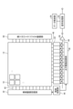
<<2. 本開示の実施形態に係る受光部30の構成例>>
次に、図2Aから図2Cを参照して、本開示の実施形態に係る受光部30の平面構成例について説明する。図2Aから図2Cは、本開示の実施形態に係る受光部30の平面構成例を示す説明図である。詳細には、図2Aに示すように、本実施形態に係る受光部30は、例えばシリコンからなる半導体基板200上に設けられた、画素アレイ部12、垂直駆動回路部32、カラム信号処理回路部34、水平駆動回路部36、出力回路部38、及び、制御回路部44等を含む。以下に、本実施形態に係る受光部30の各ブロックの詳細について説明する。
2. Configuration example of the
Next, with reference to Figures 2A to 2C, a planar configuration example of the
(画素アレイ部12)
画素アレイ部12は、半導体基板200上にマトリックス状(行方向および列方向の行列状)に2次元配置された複数の受光素子10を有する。各受光素子10は、光を電荷(例えば電子)に変換する光電変換部(フォトダイオードPD)(図示省略)と、複数の画素トランジスタ(例えばMOS(Metal-Oxide-Semiconductor)トランジスタ)(図示省略)等とを有している。言い換えると、画素アレイ部12は、入射した光を光電変換し、その結果得られた電荷に応じた信号を出力する画素を複数有する。そして、上記画素トランジスタは、例えば、転送トランジスタ、選択トランジスタ、リセットトランジスタ、及び、増幅トランジスタ等の各種機能を持ったトランジスタを含むことができる。なお、受光素子10の等価回路等の詳細については後述する。
(Pixel array section 12)
The
ここで、行方向とは、水平方向の受光素子10の配列方向をいい、列方向とは、垂直方向の受光素子10の配列方向をいう。行方向は、図2A中、左右方向であり、列方向は、図2A中、上下方向である。画素アレイ部12においては、行列状の受光素子10の配列に対して、行ごとに画素駆動配線42が行方向に沿って配線されるとともに、各列に垂直信号線48が列方向に沿って配線されている。例えば画素駆動配線42は、受光素子10から信号を読み出す際の駆動を行うための駆動信号を伝送する。Here, the row direction refers to the horizontal arrangement direction of the
(垂直駆動回路部32)
垂直駆動回路部32は、例えばシフトレジスタやアドレスデコーダ等によって形成され、画素駆動配線42を選択し、選択された画素駆動配線42に受光素子10を駆動するためのパルスを供給し、全受光素子10同時あるいは行単位で受光素子10を駆動する。例えば、垂直駆動回路部32は、画素アレイ部12の各受光素子10を行単位で順次垂直方向(図2A中の上下方向)に選択走査し、各受光素子10のフォトダイオードPDの受光量に応じて生成された電荷に基づく画素信号を、垂直信号線48を通して後述するカラム信号処理回路部34に供給する。
(Vertical drive circuit section 32)
The vertical
(カラム信号処理回路部34)
カラム信号処理回路部34は、受光素子10の列ごとに配置されており、1行分の受光素子10から出力される信号に対して列ごとにノイズ除去等の信号処理を行う。例えば、カラム信号処理回路部34は、受光素子10の固有の固定パターンノイズを除去するためにCDS(Correlated Double Sampling:相関2重サンプリング)及びAD(Analog-Degital)変換等の信号処理を行う。
(Column signal processing circuit unit 34)
The column signal
(水平駆動回路部36)
水平駆動回路部36は、例えばシフトレジスタやアドレスデコーダなどによって形成され、水平走査パルスを順次出力することによって、上述したカラム信号処理回路部34の各々を順番に選択し、カラム信号処理回路部34の各々から信号を水平信号線46に出力させることができる。
(Horizontal drive circuit section 36)
The horizontal
(出力回路部38)
出力回路部38は、上述したカラム信号処理回路部34の各々から水平信号線46を通して順次に供給される信号に対し、信号処理を行い出力することができる。出力回路部38は、例えば、バッファリング(buffering)を行う機能部として機能してもよく、もしくは、列ばらつき補正、各種デジタル信号処理等の処理を行ってもよい。なお、バッファリングとは、信号のやり取りの際に、処理速度や転送速度の差を補うために、一時的に信号を保存することをいう。
(Output circuit section 38)
The
(制御回路部44)
制御回路部44は、入力クロックと、動作モードなどを指令するデータを受け取り、また、受光素子10の内部情報等のデータを出力することができる。すなわち、制御回路部44は、垂直同期信号、水平同期信号及びマスタクロックに基づいて、垂直駆動回路部32、カラム信号処理回路部34及び水平駆動回路部36等の動作の基準となるクロック信号や制御信号を生成する。そして、制御回路部44は、生成したクロック信号や制御信号を、垂直駆動回路部32、カラム信号処理回路部34及び水平駆動回路部36等に出力する。
(Control circuit unit 44)
The
(振り分けトランジスタ駆動部50、信号処理部52、データ格納部54)
図2B及び図2Cに示すように、受光素子10には、振り分けトランジスタ駆動部50、信号処理部52、及びデータ格納部54が設けられてもよい。すなわち、振り分けトランジスタ駆動部50、信号処理部52、及びデータ格納部54は、半導体基板200上に設けられてもよい。しかしながら、本実施形態においては、これに限定されるものではなく、振り分けトランジスタ駆動部50、信号処理部52、及びデータ格納部54は、別の半導体基板(図示省略)に設けられてもよい。まずは、振り分けトランジスタ駆動部50は、後述する振り分けトランジスタVG(図3 参照)の動作を制御する。例えば、振り分けトランジスタ駆動部50は、図2Bに示すように、列方向に沿って画素アレイ部12と隣り合うように設けられてもよく、もしくは、図2Cに示すように、行方向に沿って画素アレイ部12と隣り合うように設けられていてもよく、本実施形態においては、特に限定されるものではない。また、信号処理部52は、少なくとも演算処理機能を有し、出力回路部38から出力される信号に基づいて、演算処理等の種々の信号処理を行う。データ格納部54は、信号処理部52の信号処理にあたって、その処理に必要なデータを一時的に格納する。
(Distribution
As shown in FIG. 2B and FIG. 2C, the
なお、本実施形態に係る受光部30の平面構成例は、図2Aから図2Cに示される例に限定されるものではなく、例えば、他の回路等を含んでもよく、特に限定されるものではない。
Note that the planar configuration example of the
<<3. 本開示の実施形態に係る受光素子10の等価回路>>
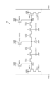
次に、図3を参照して、本開示の実施形態に係る受光素子10の等価回路について説明する。図3は、本開示の実施形態に係る受光素子10の等価回路図である。
<<3. Equivalent circuit of the
Next, an equivalent circuit of the
詳細には、図3に示すように、受光素子10は、光を電荷に変換する光電変換素子(光電変換部)としてフォトダイオードPDと、電荷排出トランジスタOFG(なお、電荷排出トランジスタOFGは、等価回路上では1つのトランジスタで示されているが、電気的に並列接続された複数のトランジスタから構成されてもよい)とを有する。さらに、受光素子10は、振り分けトランジスタVG、電荷蓄積部(第1の電荷蓄積部、第2の電荷蓄積部)MEM、転送トランジスタTG、浮遊拡散領域FD、リセットトランジスタRST、増幅トランジスタAMP、及び選択トランジスタSELをそれぞれ2個ずつ有する。3, the
図3に示すように、受光素子10においては、電荷排出トランジスタOFGのソース/ドレインの一方は、受光することで電荷を発生するフォトダイオードPDに電気的に接続される。さらに、電荷排出トランジスタOFGのソース/ドレインの他方は、電源回路(電源電位VDD)に電気的に接続される。そして、電荷排出トランジスタOFGは、自身のゲートに印加された電圧に応じて導通状態になり、フォトダイオードPDに蓄積された電荷を上記電源回路(電源電位VDD)に排出することができる。As shown in FIG. 3, in the
また、図3に示すように、受光素子10においては、振り分けトランジスタVG1、VG2のソース/ドレインの一方は、フォトダイオードPDに電気的に接続され、振り分けトランジスタVG1、VG2のソース/ドレインの他方は、電荷蓄積部MEM1、MEM2にそれぞれ電気的に接続される。そして、振り分けトランジスタVG1、VG2は、自身のゲート(第1の振り分けゲート、第2の振り分けゲート)に印加された電圧に応じて導通状態になり、フォトダイオードPDに蓄積された電荷を電荷蓄積部MEM1、MEM2にそれぞれ転送することができる。すなわち、本実施形態においては、振り分けトランジスタVG1、VG2のゲートに印加される電圧を、互いに異なるタイミングで変化させることにより、フォトダイオードPDに蓄積された電荷を2つある電荷蓄積部MEM1、MEM2のいずれかに振り分けることができる。言い換えると、2つの電荷蓄積部MEM1、MEM2は、1つのフォトダイオードPDを共有しているといえる。3, in the
また、図3に示すように、受光素子10においては、転送トランジスタTG1、TG2のソース/ドレインの一方は、振り分けトランジスタVG1、VG2のソース/ドレインの他方及び電荷蓄積部MEM1、MEM2に電気的に接続される。さらに、転送トランジスタTG1、TG2のソース/ドレインの他方は、浮遊拡散領域FD1、FD2に電気的に接続される。そして、転送トランジスタTG1、TG2は、自身のゲート(転送ゲート)に印加された電圧に応じて導通状態になり、電荷蓄積部MEM1、MEM2に蓄積された電荷を浮遊拡散領域FD1、FD2に転送することができる。なお、本開示の実施形態においては、2つの電荷蓄積部MEM1、MEM2があるため、転送トランジスタTG1、TG2は、1つの浮遊拡散領域FDを共有することも可能である。3, in the
また、浮遊拡散領域FD1、FD2は、電荷を電圧に変換して信号として出力する増幅トランジスタAMP1、AMP2のゲートに電気的に接続される。また、増幅トランジスタAMP1、AMP2のソース/ドレインの一方は、選択信号に従って、変換によって得た上記信号を信号線VSL1、VSL2に出力する選択トランジスタSEL1、SEL2のソース/ドレインの一方に電気的に接続される。さらに、増幅トランジスタAMP1、AMP2のソース/ドレインの他方は、電源回路(電源電位VDD)に電気的に接続される。The floating diffusion regions FD1 and FD2 are also electrically connected to the gates of the amplification transistors AMP1 and AMP2, which convert the charge into a voltage and output it as a signal. One of the source/drain of the amplification transistors AMP1 and AMP2 is also electrically connected to one of the source/drain of the selection transistors SEL1 and SEL2, which output the signal obtained by conversion to the signal lines VSL1 and VSL2 in accordance with a selection signal. The other of the source/drain of the amplification transistors AMP1 and AMP2 is also electrically connected to a power supply circuit (power supply potential VDD).
また、選択トランジスタSEL1、SEL2のソース/ドレインの他方は、変換された電圧を信号として伝達する上記信号線VSL1、VSL2に電気的に接続され、さらに上述したカラム信号処理回路部34に電気的に接続される。さらに、選択トランジスタSEL1、SEL2のゲートは、信号を出力する行を選択する選択線(図示省略)に電気的に接続され、さらに上述した垂直駆動回路部32に電気的に接続される。すなわち、浮遊拡散領域FD1、FD2に蓄積された電荷は、選択トランジスタSEL1、SEL2の制御により、増幅トランジスタAMP1、AMP2によって電圧に変換され、信号線VSL1、VSL2に出力されることとなる。In addition, the other of the source/drain of the selection transistors SEL1 and SEL2 is electrically connected to the signal lines VSL1 and VSL2 that transmit the converted voltage as a signal, and is further electrically connected to the above-mentioned column signal
また、図3に示すように、浮遊拡散領域FD1、FD2は、蓄積した電荷をリセットするためのリセットトランジスタRST1、RST2のドレイン/ソースの一方に電気的に接続される。リセットトランジスタRST1、RST2のゲートは、リセット信号線(図示省略)に電気的に接続され、さらに上述した垂直駆動回路部32に電気的に接続される。また、リセットトランジスタRST1、RST2のドレイン/ソースの他方は、電源回路(電源電位VDD)に電気的に接続される。そして、リセットトランジスタRST1、RST2は、自身のゲートに印加された電圧に応じて導通状態になり、浮遊拡散領域FD1、FD2に蓄積された電荷をリセット(電源回路(電源電位VDD)へ排出)することができる。
As shown in FIG. 3, the floating diffusion regions FD1 and FD2 are electrically connected to one of the drains or sources of the reset transistors RST1 and RST2 for resetting the accumulated charge. The gates of the reset transistors RST1 and RST2 are electrically connected to a reset signal line (not shown) and are further electrically connected to the vertical
なお、本実施形態に係る受光素子10の等価回路は、図3に示される例に限定されるものではなく、例えば、他の素子等を含んでもよく、特に限定されるものではない。
Note that the equivalent circuit of the
ここで、受光素子10の動作例について簡単に説明する。Here, we briefly explain an example of the operation of the
まず、受光を開始する前に、フォトダイオードPDの電荷を排出する排出動作が行われる。すなわち、電荷排出トランジスタOFG1、OFG2がオンされ、フォトダイオードPDの電荷が電源回路(電源電位VDD)に排出される。First, before light reception begins, a discharge operation is performed to discharge the charge from the photodiode PD. That is, the charge drain transistors OFG1 and OFG2 are turned on, and the charge from the photodiode PD is discharged to the power supply circuit (power supply potential VDD).
次に、受光が開始され、振り分けトランジスタVG1、VG2は、互いに異なるタイミングで動作する(例えば、差動)ように制御される。詳細には、第1の期間において、振り分けトランジスタVG1がオンすることにより、フォトダイオードPDの電荷が電荷蓄積部MEM1に転送される。一方、第2の期間においては、振り分けトランジスタVG2がオンすることにより、フォトダイオードPDの電荷が電荷蓄積部MEM2に転送される。すなわち、振り分けトランジスタVG1、VG2により、フォトダイオードPDで生成された電荷が、電荷蓄積部MEM1、MEM2に振り分けられる。Next, light reception is started, and the distribution transistors VG1 and VG2 are controlled to operate at different timings (e.g., differentially). In detail, in the first period, the distribution transistor VG1 is turned on, and the charge of the photodiode PD is transferred to the charge storage unit MEM1. On the other hand, in the second period, the distribution transistor VG2 is turned on, and the charge of the photodiode PD is transferred to the charge storage unit MEM2. That is, the distribution transistors VG1 and VG2 distribute the charge generated in the photodiode PD to the charge storage units MEM1 and MEM2.
次に、浮遊拡散領域FD1、FD2の電荷を排出する排出動作が行われる。すなわち、リセットトランジスタRST1、RST2がオンされ、浮遊拡散領域FD1、FD2の電荷が電源回路(電源電位VDD)に排出される。この後、浮遊拡散領域FD1、FD2に発生した電荷(ktcノイズ)は、CDS駆動によって除去されることが好ましい。Next, a discharge operation is performed to discharge the charge in the floating diffusion regions FD1 and FD2. That is, the reset transistors RST1 and RST2 are turned on, and the charge in the floating diffusion regions FD1 and FD2 is discharged to the power supply circuit (power supply potential VDD). After this, the charge (ktc noise) generated in the floating diffusion regions FD1 and FD2 is preferably removed by CDS driving.
そして、転送トランジスタTG1、TG2がオンされ、電荷蓄積部MEM1、MEM2に蓄積された電荷が浮遊拡散領域FD1、FD2に転送される。そして、受光期間が終了すると、画素アレイ部12の各受光素子10が、順次選択される。選択された受光素子10では、選択トランジスタSEL1、SEL2がオンされる。これにより、浮遊拡散領域FD1、FD2に蓄積された電荷が、信号として信号線VSL1、VSL2に出力される。Then, the transfer transistors TG1 and TG2 are turned on, and the charges stored in the charge storage units MEM1 and MEM2 are transferred to the floating diffusion regions FD1 and FD2. Then, when the light receiving period ends, each light receiving
なお、本実施形態に係る受光素子10の動作は、上述の例に限定されるものではなく、例えば、適宜順序が変更されてもよい。そして、本実施形態においては、2つの浮遊拡散領域FD1とFD2に蓄積される電荷の配分比から、対象物800までの距離を求めることができる。以下に、その原理について簡単に説明する。
Note that the operation of the
<<4.本開示の実施形態に係る測距モジュール1を用いた距離の算出方法の原理>>
次に、本開示の実施形態に係る測距モジュール1を用いた距離の算出方法(間接式)の原理について、図4を参照して説明する。図4は、本開示の実施形態に係る測距モジュール1を用いた距離の算出方法の原理を説明するための説明図であり、詳細には、測距モジュール1における、照射光と反射光とを強度の時間変動を模式的に示している。
<<4. Principle of distance calculation method using
Next, the principle of the distance calculation method (indirect type) using the
図4に示すように、測距モジュール1は、光の強度が周期的に変動するように変調された光を照射部20から対象物800に向かって照射する。照射された光は、対象物800で反射されて、反射光として測距モジュール1の受光部30で検出される。図4に示すように、検出された反射光(図4の上から2段目)は、照射光(図4の上から1段目)に対して位相差φをもっており、当該位相差φは、測距モジュール1から対象物800までの距離が遠ければ大きくなり、測距モジュール1から対象物800までの距離が近ければ小さくなる。As shown in Figure 4, the ranging
先に説明したように、本実施形態に係る受光素子10は、例えば互いに差動する振り分けトランジスタVG1、VG2を有している。従って、振り分けトランジスタVG1、VG2がそれぞれ動作する期間は重なっていないことから、図4中のグレーで示される領域802a、802bの期間において、フォトダイオードPDに蓄積した電荷は、電荷蓄積部MEM1、MEM2のそれぞれに振り分けられることとなる。詳細には、電荷蓄積部MEM1、MEM2のそれぞれに振り分けられた電荷は、浮遊拡散領域FD1、FD2に転送され、最終的には、領域802a、802bの期間における積分値である面積に相当する信号に変換される。従って、図4から明らかなように、領域802aの積分値と領域802bの積分値との差分は、反射光の位相差φに応じて変化する。従って、本実施形態においては、領域802aの積分値と領域802bの積分値との差分に基づいて位相差φを算出することにより、対象物800までの距離を算出することができる。なお、本実施形態においては、積分値の差分ではなく、積分値の比を用いて位相差φを算出し、距離を算出することも可能である。As described above, the
<<5. 本実施形態を創作するに至る背景>>
以上、本開示の実施形態に係る測距モジュール1、受光部30、受光素子10、及び、距離の算出方法の原理について説明した。ここで、さらに本実施形態の詳細を説明する前に、本発明者らが本実施形態を創作するに至る背景について簡単に説明する。
<<5. Background to the Creation of the Present Embodiment>>
The
先に説明したように、測距モジュール1の受光部30は、短い間隔で、受光を複数繰り返すことにより、信号量を増加させてS/N比を高め、精度の高い測距を可能にしている。例えば、当該受光部30に対しては、例えば数百MHz以上の周波数で、受光、及び発生した電荷の振り分けを行う動作を行うことが求められる。従って、受光部30の受光素子10の振り分けトランジスタVG1、VG2に対しては、低消費電力で、フォトダイオードPDで発生した電荷を高速で電荷蓄積部MEM1、MEM2へ転送(振り分ける)することが求められることとなる。As explained above, the
そこで、本発明者らは、上述のような要求を鑑みて、本開示の実施形態を創作するに至った。詳細には、本発明者らが創作した本開示の実施形態においては、振り分けトランジスタVGのゲートは、半導体基板200内に埋め込まれた一対の埋込ゲート部を有する。当該埋込ゲート部は、半導体基板200内に埋め込まれていることから、埋込ゲート部の周囲のポテンシャルを効果的に変調する。従って、埋込ゲート部によれば、半導体基板200の深い箇所にあるフォトダイオードPDで発生した電荷を、電荷蓄積部MEMへ転送することができる。さらに、本発明者らが創作した本開示の実施形態においては、振り分けトランジスタVGのゲートは、2つの埋込ゲート部を有する。従って、本実施形態によれば、2つの埋込ゲート部により、低消費電力でありつつ、より効果的に周囲のポテンシャルを変調することができ、その結果、より高速に電荷を電荷蓄積部MEMへ転送することができる。なお、埋込ゲート部によって寄生容量が増加することから消費電力が増加するが、設計を最適化して全体のバランスをとることにより、低消費電力を実現することができる。以下に、本発明者らが創作した本開示の実施形態の詳細を順次説明する。Therefore, the present inventors have created an embodiment of the present disclosure in consideration of the above-mentioned requirements. In detail, in the embodiment of the present disclosure created by the present inventors, the gate of the distribution transistor VG has a pair of buried gate portions embedded in the
<<6. 第1の実施形態>>
<6.1 平面構造>
まずは、図5を参照して、本開示の第1の実施形態に係る受光素子10の平面構造例を説明する。図5は、本実施形態に係る受光素子10の平面構成例を示す説明図であって、半導体基板200の表面の上方から受光素子10を見た場合の図となる。なお、図5における左右方向は、図2Aの行方向(左右方向)に対応し、図5における上下方向は、図2Aの列方向(上下方向)に対応するものとする。
<<6. First embodiment>>
<6.1 Planar structure>
First, an example of the planar structure of the
図5に示すように、受光素子10の中央部のP型半導体基板200内には、N型半導体領域100が形成され、N型半導体領域100は、フォトダイオード(光電変換部)PDの一部を構成する。さらに、フォトダイオードPDの中心点(中心)Oを通過し、受光素子10を上下方向(列方向)に沿って延伸する中心線600に対して、線対称(略線対称)となるように、振り分けトランジスタVG1及びVG2のゲート電極(第1の振り分けゲート、第2の振り分けゲート)150a、150bが配置されている。なお、振り分けトランジスタVG1及びVG2のゲート電極150a、150bは、N型半導体領域100の少なくとも一部と重なるように設けられている。5, an N-
詳細には、振り分けトランジスタVG1は、ゲート電極150aと、ゲート電極150aと半導体基板200との間に位置するゲート絶縁膜(図示省略)と、ソース領域としてのN型半導体領域100と、ドレイン領域としてのN型半導体領域102aとで構成される。ソース領域としてのN型半導体領域100は、フォトダイオードPDと兼用され、ドレイン領域としてのN型半導体領域102aは、電荷蓄積部MEM1と兼用されている。さらに、ゲート電極150aは、図5中の破線で示されているように、半導体基板200内に埋め込まれた一対の埋込ゲート部170a、170b(図6 参照)を有する。なお、埋込ゲート部170a、170bの詳細については後述する。また、振り分けトランジスタVG2についても、振り分けトランジスタVG1と同様である。In detail, the distribution transistor VG1 is composed of a
さらに、図5に示すように、フォトダイオードPDの中心点Oを通過し、受光素子10を左右方向(行方向)に沿って延伸する中心線602に対して、線対称(略線対称)となるように、電荷排出トランジスタOFG1及びOFG2のゲート電極152a、152bが配置されている。なお、電荷排出トランジスタOFG1及びOFG2のゲート電極152a、152bは、N型半導体領域100の少なくとも一部と重なるように設けられている。5, the
詳細には、電荷排出トランジスタOFG1は、ゲート電極152aと、ゲート電極152aと半導体基板200との間に位置するゲート絶縁膜(図示省略)と、ソース領域としてのN型半導体領域100と、ドレイン領域としてのN型半導体領域104aとで構成される。ソース領域としてのN型半導体領域100は、フォトダイオードPDと兼用される。さらに、ゲート電極152aは、図5中の破線で示されているように、半導体基板200内に埋め込まれた一対の埋込ゲート部を有する。なお、当該埋込ゲート部の詳細については後述する。また、電荷排出トランジスタOFG2についても、電荷排出トランジスタOFG1と同様である。
In detail, the charge discharge transistor OFG1 is composed of a
加えて、中心線600を基準として線対称となるように、且つ、N型半導体領域102及び振り分けトランジスタVG1、VG2を両側から挟み込みように、電荷蓄積部MEM1、MEM2と、転送トランジスタTG1、TG2とが設けられている。なお、電荷蓄積部MEM1は、転送トランジスタTG1と図5中の上下方向(列方向)に沿って隣り合うように並び、電荷蓄積部MEM2は、転送トランジスタTG2と図5中の上下方向(列方向)に沿って隣り合うように並ぶ。In addition, the charge storage units MEM1 and MEM2 and the transfer transistors TG1 and TG2 are arranged so as to be symmetrical with respect to the
詳細には、電荷蓄積部(第1の電荷蓄積部)MEM1は、例えば、電極154aと、電極154aの下方に設けられた絶縁膜(図示省略)と、当該絶縁膜の下方に設けられたN型半導体領域102aとからなる。また、転送トランジスタTG1は、ゲート電極156aと、ゲート電極156aと半導体基板200との間に位置するゲート絶縁膜(図示省略)と、ソース領域としてのN型半導体領域106aと、ドレイン領域としてのN型半導体領域108aとで構成される。また、電荷蓄積部(第2の電荷蓄積部)MEM2及び転送トランジスタTG2についても、電荷蓄積部MEM1及び転送トランジスタTG1と同様である。In detail, the charge storage unit (first charge storage unit) MEM1 is composed of, for example, an
さらに、中心線602を基準として線対称となるように、且つ、N型半導体領域102及び電荷排出トランジスタOFG1、OFG2を両側から挟み込みように、リセットトランジスタRST1、RST2、増幅トランジスタAMP1、AMP2、及び、選択トランジスタSEL1、SEL2が配置されている。なお、リセットトランジスタRST1、増幅トランジスタAMP1及び選択トランジスタSEL1は、図5中の左右方向(行方向)に沿って隣り合うように並び、リセットトランジスタRST2、増幅トランジスタAMP2及び選択トランジスタSEL2も、図5中の左右方向(行方向)に沿って隣り合うように並ぶ。Furthermore, the reset transistors RST1, RST2, the amplification transistors AMP1, AMP2, and the selection transistors SEL1, SEL2 are arranged so as to be linearly symmetrical with respect to the
詳細には、リセットトランジスタRST1は、ゲート電極158aと、ゲート電極158aと半導体基板200との間に位置するゲート絶縁膜(図示省略)と、ソース領域としてのN型半導体領域110aと、ドレイン領域としてのN型半導体領域112aとで構成される。ソース領域としてのN型半導体領域110aは、浮遊拡散領域FD1と兼用され、ドレイン領域としてのN型半導体領域112aは、増幅トランジスタAMP1と兼用されている。また、リセットトランジスタRST2についても、リセットトランジスタRST1と同様である。In detail, the reset transistor RST1 is composed of a
また、増幅トランジスタAMP1は、ゲート電極160aと、ゲート電極160aと半導体基板200との間に位置するゲート絶縁膜(図示省略)と、ドレイン領域としてのN型半導体領域112aと、ソース領域としてのN型半導体領域114aとで構成される。ドレイン領域としてのN型半導体領域112aは、リセットトランジスタRST1のドレイン領域と兼用されている。また、増幅トランジスタAMP2についても、増幅トランジスタAMP1と同様である。
The amplification transistor AMP1 is composed of a
さらに、選択トランジスタSEL1は、ゲート電極162aと、ゲート電極162aと半導体基板200との間に位置するゲート絶縁膜(図示省略)と、ドレイン領域としてのN型半導体領域114aと、ソース領域としてのN型半導体領域116aとで構成される。ドレイン領域としてのN型半導体領域114aは、増幅トランジスタAMP1のソース領域と兼用されている。また、選択トランジスタSEL2についても、選択トランジスタSEL1と同様である。
Furthermore, the selection transistor SEL1 is composed of a
なお、本実施形態に係る受光素子10の平面構造は、図5に示される例に限定されるものではなく、例えば、他の素子等を含んでもよく、特に限定されるものではない。
Note that the planar structure of the
<6.2 断面構造>
次に、図6から図9を参照して、本開示の第1の実施形態に係る受光素子10の断面構造例を説明する。図6は、図5のA―A´線に沿って受光素子10を切断した際の断面図であり、詳細には、図6中の上側が半導体基板200の裏面側となり、図6中の下側が半導体基板200の表面側となる。また、図7は、図5のB―B´線に沿って受光素子10を切断した際の断面図であり、図7中の上側が半導体基板200の表面側となり、図7中の下側が半導体基板200の裏面側となる。さらに、図8は、本実施形態を説明するための説明図である。そして、図9は、図6の領域Dの拡大図であって、図9中の上側が半導体基板200の表面側となり、図9中の下側が半導体基板200の裏面側となる。
<6.2 Cross-sectional structure>
Next, with reference to FIG. 6 to FIG. 9, a cross-sectional structure example of the
まずは、図6に示すように、受光素子10は、シリコン基板等からなる半導体基板200を有する。詳細には、P型の半導体基板200内には、N型半導体領域100a、100bを形成されることにより、半導体基板200内にフォトダイオードPDが形成される。6, the
次に、図6中の上側、すなわち、半導体基板200の裏面側から説明する。半導体基板200の裏面の上方には、対象物800からの反射光が入射される、スチレン系樹脂、アクリル系樹脂、スチレンーアクリル共重合系樹脂、またはシロキサン系樹脂等からなるオンチップレンズ208が設けられている。オンチップレンズ208の下方には、例えば、酸化シリコン(SiO2)、窒化シリコン(SiN)、酸窒化シリコン(SiON)等からなる平坦化膜204が設けられている。さらに、平坦化膜204の下方には、絶縁膜からなる反射防止膜202が設けられている。例えば、反射防止膜202は、酸化ハフニウム(HfO2)、酸化アルミニウム(Al2O3)、酸化チタン(TiO2)、酸化シリコン等、もしくは、これらの積層から形成することができる。
Next, the upper side in FIG. 6, that is, the back surface side of the
反射防止膜202の上方であって、隣接する受光素子10との境界領域には、対象物800からの反射光が隣接する受光素子10への入射を防止する遮光膜206が設けられている。遮光膜206は、光を遮るような材料からなり、例えば、タングステン(W)、アルミニウム(Al)、銅(Cu)等の金属材料を用いて形成することができる。Above the
さらに、遮光膜206の下方には、半導体基板200を貫通し、隣接する受光素子10へと入射光が入り込むことを防止するための画素分離部(第1の画素分離部)210(FFTI)が設けられている。当該画素分離部210は、例えば、半導体基板200の裏面から表面まで貫通するトレンチと、当該トレンチに埋め込まれた酸化シリコン等の絶縁膜又はアルミニウム等の金属膜とからなる。Furthermore, below the light-shielding
次に、図6中の下側、すなわち、半導体基板200の表面側を説明する。N型半導体領域100bを挟むようにして、縦型トランジスタである2つの振り分けトランジスタVG1、VG2が形成されている。詳細には、振り分けトランジスタVG1、VG2は、半導体基板200の表面上に設けられた、例えばポリシリコン膜からなるゲート電極150a、150bをそれぞれ有する。さらに、ゲート電極150a、150bは、半導体基板200内へ、半導体基板200の厚み方向に沿って延伸する、例えばポリシリコン膜からなる埋込ゲート部170a、170bをそれぞれ有する。言い換えると、埋込ゲート部170a、170bは、半導体基板200内に埋め込まれており、ゲート絶縁膜(図示省略)を介して半導体基板200に接しているといえる。例えば、振り分けトランジスタVG1、VG2の埋込ゲート部170a、170bは、半導体基板200の表面側からドライエッチングによってトレンチを形成し、ゲート絶縁膜を形成し、さらに、トレンチにポリシリコン膜等を埋め込むことで形成することができる。なお、本実施形態に係る埋込ゲート部170a、170bの詳細については、後述する。Next, the lower side in FIG. 6, that is, the surface side of the
なお、埋込ゲート部170a、170bに挟まれたN型半導体領域100bは、フォトダイオードPDを構成するN型半導体領域100aに比べて、不純物濃度が高いことが好ましく、さらには、N型半導体領域100bも、半導体基板200の表面側に近づくにつれて不純物濃度が高くなることが好ましい。In addition, it is preferable that the N-
さらに、振り分けトランジスタVG1、VG2を左右方向から挟み込むようにして、半導体基板200内に電荷蓄積部MEM1、MEM2が設けられている。例えば、電荷蓄積部MEM1、MEM2は、金属膜又はポリシリコン膜からなる電極154a、154bと、酸化膜からなる絶縁膜(図示省略)と、N型半導体領域102a、102b(図6中では、MEM1、MEM2として示されている)との積層からなるMOS(Metal-Oxide-Semiconductor)型容量であることができる。Furthermore, charge storage units MEM1 and MEM2 are provided in the
そして、電荷蓄積部MEM1、MEM2に隣接して、転送トランジスタTG1、TG2のゲート電極156a、156bが、半導体基板200の表面上に設けられている。さらに、転送トランジスタTG1、TG2のゲート電極156a、156bに近接した半導体基板200内に、浮遊拡散領域FD1、FD2として図示されているN型半導体領域110a、110bが形成されている。Adjacent to the charge storage units MEM1 and MEM2, the
さらに、半導体基板200の表面上には、配線層300が設けられている。配線層300は、絶縁膜302と金属膜304とを含む。さらに、配線層300の、半導体基板200と反対側の面上には、電極306が設けられている。Furthermore, a
加えて、配線層300の、半導体基板200と反対側の面上には、基板400が設けられている。基板400も、絶縁膜402と金属膜404とを含み、配線層300側の面上には、電極406が設けられている。例えば、配線層300の電極306と、基板400の電極406とは、銅(Cu)等で形成され、互いに接することで、配線層300と基板400とを接合することができる。In addition, a
なお、本実施形態に係る受光素子10の断面構造は、図6に示される例に限定されるものではなく、例えば、他の素子等を含んでもよく、特に限定されるものではない。
Note that the cross-sectional structure of the
次に、図7を参照して、本実施形態に係る埋込ゲート部170a、170bの詳細について説明する。図7は、先に説明したように、図5のB―B´線に沿って受光素子10を切断した際の断面図であり、詳細には、振り分けトランジスタVG2のゲート電極150bと、埋込ゲート部170b-1、170b-2との断面図である(なお、図7においては、ゲート絶縁膜の図示を省略している)。図7に示すように、本実施形態においては、振り分けトランジスタVG2のゲート電極150bは、図5中における上下方向、すなわち、図2Aの列方向に沿って並ぶ、一対の埋込ゲート部170b-1、170b-2を有する。さらに、埋込ゲート部170b-1、170b-2は、図5の破線で示すように、半導体基板200の表面に沿って受光素子10を切断した断面において、フォトダイオードPDの中心点Oから電荷蓄積部MEM2へ向かう方向に沿って伸びる長辺L(図9 参照)を持つ略矩形状の形状を持つことが好ましい。また、振り分けトランジスタVG1のゲート電極150aについても、振り分けトランジスタVG2のゲート電極150bと同様に、図5中における上下方向、すなわち、図2Aの列方向に沿って並ぶ、一対の埋込ゲート部170を有する。さらに、振り分けトランジスタVG1のゲート電極150aの埋込ゲート部170も、図5の破線で示すように、半導体基板200の表面に沿って受光素子10を切断した断面において、フォトダイオードPDの中心点Oから電荷蓄積部MEM2へ向かう方向に沿って伸びる長辺L(図9 参照)を持つ略矩形状の形状を持つことが好ましい。Next, the details of the buried
詳細には、本実施形態においては、図8に示すように、ゲート電極150bを介して埋込ゲート部170b-1、170b-2に対して電圧を印加することにより、埋込ゲート部170b-1、170b-2の周囲700のP型半導体領域を変調させる。そして、図9に示すように、半導体基板200の深い箇所にあるフォトダイオードPDで発生した電荷(電子)は、埋込ゲート部170bによって変調された半導体基板200内の周囲700を通過して電荷蓄積部MEM2へ転送されることとなる。本実施形態においては、2つの埋込ゲート部170b-1、170b-2により、低消費電力でありつつ、より効果的に周囲700のポテンシャルを変調することができることから、より高速に電荷を電荷蓄積部MEM2へ転送することができる。
In detail, in this embodiment, as shown in FIG. 8, a voltage is applied to the buried
さらに、本実施形態においては、埋込ゲート部170b-1、170b-2を、フォトダイオードPDの中心点Oから電荷蓄積部MEM2へ向かう方向に沿って伸びる長辺L(図9 参照)を持つ略矩形状の形状に形成する。このようにすることで、上記長辺Lの伸びる方向と電荷が移動する方向とは同じであることから、埋込ゲート部170bは電荷が通過する領域を効果的に変調し、当該変調された領域に沿って電荷を電荷蓄積部MEM2へ誘導することができる。Furthermore, in this embodiment, the buried
また、本実施形態においては、図5の破線で示すように、電荷排出トランジスタOFG1、OFG2のゲート電極152a、152bも、半導体基板200に埋め込まれ、ゲート絶縁膜(図示省略)を介して半導体基板200に接している一対の埋込ゲート部170を有していてもよい。このようにすることで、本実施形態においては、電荷排出トランジスタOFG1、OFG2のゲート電極152a、152bの2つの埋込ゲート部170により、低消費電力で、より効果的に周囲のポテンシャルを変調し、より高速に電荷を排出することができる。5, the
さらに、電荷排出トランジスタOFG1、OFG2のゲート電極152a、152bの埋込ゲート部170も、図5の破線で示すように、半導体基板200の表面に沿って受光素子10を切断した断面において、フォトダイオードPDの中心点Oから電源回路(電源電位VDD)に接続されるN型半導体領域104a、104bへ向かう方向に沿って伸びる長辺を持つ略矩形状の形状を持つことが好ましい。このようにすることで、電荷が移動する領域をより効果的に変調することができることから、より高速に、電荷を排出することができる。
Furthermore, it is preferable that the buried
すなわち、本実施形態によれば、高速で電荷を転送することができる受光素子10を提供することができる。In other words, according to this embodiment, a
<6.3 変形例>
上述した本開示の第1の実施形態に係る受光素子10は、以下のように変形することもできる。以下に、本実施形態の変形例1から変形例7を説明する。なお、以下に説明する変形例1から変形例7に係る受光素子10は、いずれも、振り分けトランジスタVGのゲート電極150は、一対の埋込ゲート部170を有する。
6.3 Modifications
The
(変形例1)
まずは、変形例1を、図10を参照して説明する。図10は、本実施形態の変形例1に係る受光素子10の平面構成例を示す説明図である。本変形例においても、振り分けトランジスタVG1、VG2のゲート電極150a、150bは、一対の埋込ゲート部170を有する。さらに、本変形例においては、図10の破線で示すように、各埋込ゲート部170は、半導体基板200の表面に沿って受光素子10を切断した断面において、フォトダイオードPDの中心点Oから電荷蓄積部MEM1、MEM2へ向かう方向に沿って伸びる長軸を持つ略楕円形の形状を持つ。本変形例においては、埋込ゲート部170を、フォトダイオードPDの中心点Oから電荷蓄積部MEM1、MEM2へ向かう方向に沿って伸びる長軸を持つ略楕円状の形状に形成することにより、上述した第1の実施形態と同様に、より高速に、電荷を電荷蓄積部MEM1、MEM2へ誘導することができる。
(Variation 1)
First, the first modification will be described with reference to FIG. 10. FIG. 10 is an explanatory diagram showing a planar configuration example of the
なお、本変形例においても、電荷排出トランジスタOFG1、OFG2のゲート電極152a、152bも、半導体基板200に埋め込まれた一対の埋込ゲート部170を有していてもよい。さらに、本変形例においては、電荷排出トランジスタOFG1、OFG2のゲート電極152a、152bの埋込ゲート部170も、図10の破線で示すように、半導体基板200の表面に沿って受光素子10を切断した断面において、フォトダイオードPDの中心点Oから電源回路(電源電位VDD)に接続されるN型半導体領域104a、104bへ向かう方向に沿って伸びる長軸を持つ略楕円状の形状を持つことができる。In this modification, the
加えて、本変形例1では、中心線600を基準として鏡面対称となるように、且つ、N型半導体領域102及び振り分けトランジスタVG1、VG2を両側から挟み込みように、電荷蓄積部MEM1、MEM2と、転送トランジスタTG1、TG2とが設けられている。なお、電荷蓄積部MEM1は、転送トランジスタTG1と図10中の上下方向(列方向)に沿って隣り合うように並び、電荷蓄積部MEM2は、転送トランジスタTG2と図10中の上下方向(列方向)に沿って隣り合うように並ぶ。In addition, in this modified example 1, the charge storage units MEM1 and MEM2 and the transfer transistors TG1 and TG2 are provided so as to be mirror symmetrical with respect to the
さらに、本変形例1においては、中心線602を基準として鏡面対称となるように、且つ、N型半導体領域102及び電荷排出トランジスタOFG1、OFG2を両側から挟み込みように、リセットトランジスタRST1、RST2、増幅トランジスタAMP1、AMP2、及び、選択トランジスタSEL1、SEL2が配置されている。なお、リセットトランジスタRST1、増幅トランジスタAMP1及び選択トランジスタSEL1は、図10中の左右方向(行方向)に沿って隣り合うように並び、リセットトランジスタRST2、増幅トランジスタAMP2及び選択トランジスタSEL2も、図10中の左右方向(行方向)に沿って隣り合うように並ぶ。Furthermore, in this modified example 1, the reset transistors RST1, RST2, the amplifier transistors AMP1, AMP2, and the select transistors SEL1, SEL2 are arranged in mirror symmetry with respect to the
(変形例2)
次に、変形例2を、図11を参照して説明する。図11は、本実施形態の変形例2に係る受光素子10の平面構成例を示す説明図である。本変形例においても、振り分けトランジスタVG1、VG2のゲート電極150a、150bは、一対の埋込ゲート部170を有する。さらに、本変形例においては、各埋込ゲート部170は、図11の破線で示すように、半導体基板200の表面に沿って受光素子10を切断した断面において、略円状の形状を持つ。本変形例においては、埋込ゲート部170を、略円状の形状に形成することにより、製造による形状のばらつきが生じることを避けることから、2つの振り分けトランジスタVG1、VG2による電荷の振り分けの性能を互いに等しく調整することができる。
(Variation 2)
Next, the second modification will be described with reference to FIG. 11. FIG. 11 is an explanatory diagram showing a planar configuration example of the
なお、本変形例においても、電荷排出トランジスタOFG1、OFG2のゲート電極152a、152bも、半導体基板200に埋め込まれた一対の埋込ゲート部170を有していてもよい。さらに、本変形例においては、ゲート電極152a、152bの埋込ゲート部170も、図11の破線で示すように、半導体基板200の表面に沿って受光素子10を切断した断面において略円状の形状を持つことができる。In this modification, the
(変形例3)
次に、変形例3を、図12を参照して説明する。図12は、本実施形態の変形例3に係る受光素子10の断面構成例を示す説明図である。本変形例においても、振り分けトランジスタVG1、VG2のゲート電極150a、150bは、一対の埋込ゲート部170a、170bを有する。さらに、本変形例においては、図12に示すように、受光素子10は、半導体基板200の、裏面(表面と反対側の面)に設けられた、微細な凹凸が形成されたモスアイ構造202aを有する。詳細には、モスアイ構造202aは、図12に示すように、半導体基板200側に頂点を有する複数の略四角錐がマトリクス状にならぶことにより構成される。本変形例においては、モスアイ構造202aを設けることにより、界面における急激な屈折率の変化を緩和し、反射を防止することができる。
(Variation 3)
Next, the third modification will be described with reference to FIG. 12. FIG. 12 is an explanatory diagram showing a cross-sectional configuration example of the
(変形例4)
次に、変形例4を、図13を参照して説明する。図13は、本実施形態の変形例4に係る受光素子10の断面構成例を示す説明図である。本変形例においても、振り分けトランジスタVG1、VG2のゲート電極150a、150bは、一対の埋込ゲート部170a、170bを有する。さらに、本変形例においては、図13に示すように、受光素子10は、半導体基板200の厚み方向に沿って、半導体基板200の裏面(表面と反対側の面)から、半導体基板200の途中まで貫く、画素分離部(第2の画素分離部)210a(DTI(deep Trench Isolation)を有する。当該画素分離部210aによれば、隣接する受光素子10へと入射光が入り込むことを防止することができる。
(Variation 4)
Next, the fourth modification will be described with reference to FIG. 13. FIG. 13 is an explanatory diagram showing a cross-sectional configuration example of the
(変形例5)
次に、変形例5を、図14を参照して説明する。図14は、本実施形態の変形例5に係る受光素子10の断面構成例を示す説明図である。本変形例においても、振り分けトランジスタVG1、VG2のゲート電極150a、150bは、一対の埋込ゲート部170a、170bを有する。さらに、本変形例においては、半導体基板200内のN型半導体領域102a、102bに埋め込まれた縦型の電極154a、154bを有する電荷蓄積部MEM1、MEM2を有する。本変形例によれば、電荷蓄積部MEM1、MEM2が縦型の電極を持つことから、当該縦型の電極と、当該電極に対向するN型半導体領域102a、102bとにはさまれた絶縁膜(図示省略)の面積を広くすることができる。その結果、本変形例によれば、面積が広くなることから、電荷蓄積部MEM1、MEM2の容量をさらに大きくすることができ、ひいては、広い受光素子10のダイナミックレンジを確保することが可能となる。
(Variation 5)
Next, the fifth modification will be described with reference to FIG. 14. FIG. 14 is an explanatory diagram showing a cross-sectional configuration example of the
(変形例6)
次に、変形例6を、図15を参照して説明する。図15は、本実施形態の変形例6に係る受光素子10の一部の断面構成例を示す説明図であり、図7の断面図に対応する。本変形例においても、振り分けトランジスタVG2のゲート電極150bは、一対の埋込ゲート部170b-1、170b-2を有する。さらに、本変形例においては、図15に示すように、各埋込ゲート部170b-1、170b-2は、半導体基板200の表面から、当該表面の反対側に位置する裏面に向かう半導体基板200の厚み方向において、漸次狭くなるテーパ形状を持つ。言い換えると、本変形例においては、一対の埋込ゲート部170b-1、170b-2の、互いに向かい合う側面の間の距離(幅)は、半導体基板200の表面から、当該表面の反対側に位置する裏面に向かう半導体基板200の厚み方向において、漸次広がっている。
(Variation 6)
Next, the sixth modification will be described with reference to FIG. 15. FIG. 15 is an explanatory diagram showing a cross-sectional configuration example of a part of the
本変形例においては、一対の埋込ゲート部170b-1、170b-2の、互いに向かい合う側面の間の距離を、半導体基板200の表面から半導体基板200の厚み方向に沿って、漸次広げることにより、半導体基板200の厚み方向に好適なポテンシャル勾配を生成し、転送する電荷を半導体基板200の表面近傍に集まりやすくする。そして、本変形例においては、電荷を半導体基板200の表面近傍に集め、転送することにより、安定した電荷の振り分け動作を行うことができ、測距の精度を向上させることができる。In this modification, the distance between the opposing side surfaces of a pair of buried
例えば、図15に示すように、各埋込ゲート部170b-1、170b-2は、半導体基板200の表面から半導体基板200の厚み方向に沿って、各埋込ゲート部170b-1、170b-2の長さ(深さ)に対して3/4進んだ箇所の直径L2が、半導体基板200の表面での直径L1に対して、3/4程度となることが好ましい。このようにすることで、埋込ゲート部170b-1、170b-2を形成する際に、埋込ゲート部170b-1、170b-2に空洞(Void)が生成されることを避け、埋め込み性を良好に維持することができる。15, it is preferable that the diameter L2 of each of the buried
(変形例7)
次に、変形例7を、図16を参照して説明する。図16は、本実施形態の変形例7に係る受光素子10の断面構成例を示す説明図である。本変形例においては、図16に示すように、受光素子10は、複数の、詳細には、4つの振り分けトランジスタVGを有してもよい。本変形例においても、各振り分けトランジスタVGのゲート電極(第3の振り分けゲート)150は、一対の埋込ゲート部170を有し、それぞれ電荷蓄積部(第3の電荷蓄積部)MEMへ電荷を振り分けることができる。なお、本変形例においても、電荷排出トランジスタOFGのゲート電極152も、半導体基板200に埋め込まれた一対の埋込ゲート部を有していてもよい。
(Variation 7)
Next, the seventh modification will be described with reference to FIG. 16. FIG. 16 is an explanatory diagram showing a cross-sectional configuration example of the
<<7. 第2の実施形態>>
ところで、上述した本開示の第1の実施形態においては、振り分けトランジスタVGには、半導体基板200に埋め込まれた一対の埋込ゲート部170を有することにより大きな寄生容量が発生する。そして、このような大きな寄生容量により、振り分けトランジスタVGによる電荷の転送の速度が遅くなる場合がある。そこで、以下に説明する本開示の第2の実施形態においては、振り分けトランジスタVGのゲート電極150の寄生容量を小さくするために、埋込ゲート部170の、電荷を転送する際に機能する部分以外の部分に接するように低誘電体層を設けている。以下に、本実施形態の詳細を順次説明する。
<<7. Second embodiment>>
Incidentally, in the first embodiment of the present disclosure described above, a large parasitic capacitance occurs in the distribution transistor VG due to the pair of buried
<7.1 実施形態>
まずは、図17及び図18を参照して、本実施形態に係る振り分けトランジスタVGの埋込ゲート部170を説明する。図17は、本実施形態に係る受光素子10を説明するための説明図であり、図7の断面図に対応する。図18は、本実施形態に係る受光素子10の平面構成例を示す説明図であり、詳細には、半導体基板200の表面において、説明の便宜上、ゲート電極150等の図示を省略した図である。
7.1 Embodiment
First, the buried
本実施形態においては、図17及び図18に示すように、一対の埋込ゲート部170b-1、170b-2のうち、一方の埋込ゲート部170b-1の、他方の埋込ゲート部170b-2と向かいあう側面とは反対側に位置する側面は、低誘電体層172b-1、172b-2に接する。当該低誘電体層172bは、例えば酸化膜(例えばSiO2)又は窒化膜(例えばSiN)から形成することができる。このように、本実施形態においては、埋込ゲート部170の、電荷を転送する際に機能する部分以外の部分に接するように低誘電体層172を設けることにより、ゲート電極150の寄生容量の増加を抑えることができる。その結果、本実施形態においては、振り分けトランジスタVGによる電荷の転送の速度が遅くなることを避けることができる。
In this embodiment, as shown in FIG. 17 and FIG. 18, the side of one of the pair of buried
なお、本実施形態においては、図18に示すように、電荷排出トランジスタOFGのゲート電極152も、半導体基板200に埋め込まれた一対の埋込ゲート部174を有してもよい。さらに、電荷排出トランジスタOFGのゲート電極152の一対の埋込ゲート部174a、174bについても、一方の埋込ゲート部174b-1の、他方の埋込ゲート部174b-2と向かいあう側面とは反対側に位置する側面は、低誘電体層176b-1、176b-2に接してもよい。当該低誘電体層176bも、例えば酸化膜又は窒化膜から形成することができる。このようにすることで、電荷排出トランジスタOFGのゲート電極152の寄生容量の増加を抑え、電荷排出トランジスタOFGによる電荷の排出の速度が遅くなることを避けることができる。
In this embodiment, as shown in FIG. 18, the gate electrode 152 of the charge discharge transistor OFG may also have a pair of buried gate portions 174 buried in the
<7.2 変形例>
なお、上述した本開示の第2の実施形態に係る受光素子10は、以下のように変形することもできる。以下に、図19及び図20を参照して、本実施形態の変形例1及び2を説明する。図19は、本実施形態の変形例1に係る受光素子10の平面構成例を示す説明図であり、図20は、本実施形態の変形例2に係る受光素子10の平面構成例を示す説明図である。なお、図19及び図20は、図18と同様に、半導体基板200の表面において、説明の便宜上、ゲート電極150等の図示を省略した図である。
7.2 Modifications
The
図19及び図20に示すように、これら変形例においては、埋込ゲート部170の一方の側面は、低誘電体層178に接しており、当該低誘電体層178は、半導体基板200上の各要素を電気的に分離するための素子分離部からなる。また、これら変形例においては、図19及び図20に示すように、電荷排出トランジスタOFGのゲート電極152の一対の埋込ゲート部174a、174bについても、一方の側面は、低誘電体層178に接しており、当該低誘電体層178は、半導体基板200上の各要素を電気的に分離するための素子分離部からなる。19 and 20, in these modified examples, one side of the buried
<7.3 製造方法>
次に、図21Aから図21Fを参照して本実施形態に係る埋込ゲート部170及び低誘電体層178の製造方法の一例について説明する。図21Aから図21Fは、本実施形態に係る受光素子10の製造方法を説明するための説明図である。
<7.3 Manufacturing method>
Next, an example of a method for manufacturing the buried
まずは、図21Aに示すように、半導体基板200の表面に、熱酸化による熱酸化シリコン層500を形成する。さらに、熱酸化シリコン層500上に、窒化シリコン層502と、酸化シリコン層504と、パターニングされたレジスト506とを形成する。First, as shown in Fig. 21A, a thermally oxidized
次に、レジスト506のパターンに沿ってドライエッチングを行い、酸化シリコン層504を剥離すると、図21Bに示すようなトレンチ510が形成される。Next, dry etching is performed along the pattern of resist 506 to remove
そして、熱酸化を行い、トレンチ510内の底面及び側面に熱酸化シリコン層500を形成し、さらに、図21Cに示すように、トレンチ510内に酸化シリコン膜(低誘電体層)172を埋め込む。Then, thermal oxidation is performed to form a thermally oxidized
さらに、図21Dに示すように、パターニングされたレジスト508を形成する。 Further, as shown in FIG. 21D, a patterned resist 508 is formed.
次に、図21Eに示すように、レジスト508のパターンに沿って、酸化シリコン膜172に対してドライエッチングを行い、トレンチ512が形成される。Next, as shown in FIG. 21E, dry etching is performed on the
そして、トレンチ512にポリシリコン膜(埋込ゲート部)170、150を埋め込み、レジスト508及び窒化シリコン層502を剥離することにより、図21Fに示すような構造を得ることができる。Then, polysilicon films (buried gate portions) 170, 150 are embedded in the
以上のように、本実施形態によれば、一方の埋込ゲート部170の、他方の埋込ゲート部170と向かいあう側面とは反対側に位置する側面に接するように、低誘電体層178を形成することにより、振り分けトランジスタVGのゲート電極150の寄生容量を小さくすることができる。As described above, according to this embodiment, the parasitic capacitance of the
<<8. 第3の実施形態>>
また、上述の第1及び第2の実施形態及びその変形例においては、電荷蓄積部MEM1、MEM2の絶縁膜(図示省略)や、増幅トランジスタAMP1、AMP2のゲート絶縁膜(図示省略)等を薄膜化してもよい。このようにすることで、サイズを大きくすることなく、電荷蓄積部MEM1、MEM2の容量を増加させることができる。さらに、ゲート絶縁膜内の結晶欠陥が少なくなったり、トランジスタの相互コンダクタンスgmが大きくなることにより結晶欠陥の影響が小さくなったり、熱処理時間短縮や熱処理温度の低温化により界面準位が少なくなることから、増幅トランジスタAMP1、AMP2のランダムノイズを低減することができる。
<<8. Third embodiment>>
In the above-described first and second embodiments and their modified examples, the insulating film (not shown) of the charge storage units MEM1 and MEM2 and the gate insulating film (not shown) of the amplifying transistors AMP1 and AMP2 may be thinned. In this way, the capacitance of the charge storage units MEM1 and MEM2 can be increased without increasing the size. Furthermore, random noise of the amplifying transistors AMP1 and AMP2 can be reduced because the number of crystal defects in the gate insulating film is reduced, the influence of crystal defects is reduced by increasing the mutual conductance gm of the transistor, and the interface state is reduced by shortening the heat treatment time and lowering the heat treatment temperature.
ここで、図22、図23A、及び図23Bを参照して、薄膜化された絶縁膜を有する電荷蓄積部MEM1、MEM2及び増幅トランジスタAMP1、AMP2についての、本開示の第3の実施形態を説明する。なお、図22は、本実施形態に係る受光素子10の平面構成例を示す説明図であって、半導体基板200の表面の上方から受光素子10を見た場合の図となり、第1の実施形態の受光素子10と同様である。また、図23Aは、図22のC―C´線に沿って受光素子10を切断した際の断面図であり、図23Bは、図22のD-D´線に沿って受光素子10を切断した際の断面図である。詳細には、図23A及び図23Bにおいては、図中の上側が半導体基板200の表面側となり、図中の下側が半導体基板200の裏面側となる。Here, the third embodiment of the present disclosure will be described with reference to FIG. 22, FIG. 23A, and FIG. 23B, with respect to the charge storage units MEM1 and MEM2 and the amplifying transistors AMP1 and AMP2 having a thinned insulating film. FIG. 22 is an explanatory diagram showing a planar configuration example of the
詳細には、本実施形態においては、例えば、図23Aに示すように、増幅トランジスタAMP1の、サイドウォール730に覆われたゲート電極160の下方に位置する絶縁膜720aは、例えば酸化膜(第3の酸化膜)からなり、その膜厚は、リセットトランジスタRST1のゲート電極158及び選択トランジスタSEL1のゲート電極162の下方に位置する、酸化膜(第3の酸化膜)からなる絶縁膜720に比べて薄い。In detail, in this embodiment, for example, as shown in FIG. 23A, the insulating
また、本実施形態においては、例えば、図23Bに示すように、電荷蓄積部MEM1の、サイドウォール730に覆われた電極154の下方に位置する絶縁膜720aは、例えば酸化膜(第1の酸化膜)からなり、その膜厚は、転送トランジスタTG1のゲート電極156の下方に位置する、酸化膜(第2の酸化膜)からなる絶縁膜720に比べて薄い。
In addition, in this embodiment, for example, as shown in FIG. 23B, the insulating
なお、本実施形態においては、増幅トランジスタAMP1のゲート電極160の下方に位置する絶縁膜720a及び電荷蓄積部MEM1の電極154の下方に位置する絶縁膜720aは、同一材料からなる酸化膜であってもよく、また、略同一の膜厚をもっていてもよい。In this embodiment, the insulating
より具体的には、本実施形態においては、増幅トランジスタAMP1のゲート電極160の下方に位置する絶縁膜720a及び電荷蓄積部MEM1の電極154の下方に位置する絶縁膜720aは、酸化シリコン(SiO2)、窒化シリコン(SiN)等の酸化膜からなる。また、本実施形態においては、増幅トランジスタAMP1のゲート電極160の下方に位置する絶縁膜720a及び電荷蓄積部MEM1の電極154の下方に位置する絶縁膜720aの膜厚は、薄くなることによる、ランダムノイズの低減効果、及び、リーク電流の増加による消費電力の増加を鑑みて、他の素子(転送トランジスタTG、リセットトランジスタRST及び選択トランジスタSEL)のゲート電極156、158、162の下方に位置する絶縁膜720の膜厚の半分程度であることが好ましく、例えば、1.0nm以上、5.0nm以下であることがより好ましい。
More specifically, in this embodiment, the insulating
さらに、本実施形態においては、増幅トランジスタAMP1のゲート電極160の下方に位置する絶縁膜720a及び電荷蓄積部MEM1の電極154の下方に位置する絶縁膜720aは、半導体基板200の上方から見た場合、隣接する素子を干渉しない程度に、ゲート電極160及び電極154に比べて広くなっていることが好ましい。
Furthermore, in this embodiment, it is preferable that the insulating
なお、本実施形態においては、電荷蓄積部MEM1、MEM2の絶縁膜720aや、増幅トランジスタAMP1、AMP2のゲート絶縁膜720aのみを薄膜化することに限定されるものではない。本実施形態においては、電荷蓄積部MEM1、MEM2の絶縁膜720aのみを薄膜化してもよく、受光素子10上の素子(電荷蓄積部MEM、転送トランジスタTG、振り分けトランジスタVG、電荷排出トランジスタOFG、増幅トランジスタAMP、リセットトランジスタRST及び選択トランジスタSEL)のゲート電極150、152、154、156、158、160、162及び電極154に接する絶縁膜720を薄膜化してもよい。In this embodiment, it is not limited to thinning only the insulating
以上のように、本実施形態によれば、電荷蓄積部MEMの絶縁膜720aや、増幅トランジスタAMPのゲート絶縁膜720a等を薄膜化することにより、サイズを大きくすることなく、電荷蓄積部MEMの容量を増加させ、トランジスタのランダムノイズを低減することができる。従って、本実施形態においては、上述した第1の実施形態に係る構成により、高速で電荷を転送することができ、さらに、第3の実施形態に係る構成により、転送した電荷を蓄積するための電荷蓄積部MEMの容量を増加させることができることから、より測距精度の高い測距モジュール1を得ることができる。加えて、第3の実施形態に係る構成により、トランジスタのランダムノイズの低減を行うことができるため、測距モジュール1の特性をより向上させることができる。なお、本実施形態は、上述した第1及び第2の実施形態及びその変形例と組み合わせて実施することができる。As described above, according to this embodiment, the insulating
<<9. 第4の実施形態>>
ところで、上述の第3の実施形態においては、電荷蓄積部MEMの絶縁膜720aや、増幅トランジスタAMPのゲート絶縁膜720a等を薄膜化し、電荷蓄積部MEMの容量を増加させ、増幅トランジスタAMPのランダムノイズを低減していた。しかしながら、ゲート絶縁膜720aの薄膜化を進めた場合、上述のような効果を得られるものの、リーク電流が増加してしまうため、薄膜化にも限界がある。そこで、本発明者らは、同じ膜厚であっても、上述の酸化膜に比べて、電荷蓄積部MEMの容量を増加させることができる高い比誘電率を持つ高誘電体膜を上記絶縁膜720aの代わりに使用することを着想した。上記絶縁膜720aとして高誘電体膜を使用することにより、膜厚を薄くしても、リーク電流の増加を避けつつ、電荷蓄積部MEMの容量の増加や、増幅トランジスタAMPのランダムノイズの低減を両立することができる。
<<9. Fourth embodiment>>
In the above-mentioned third embodiment, the insulating
ここで、図24、図25A、及び図25Bを参照して、高誘電体膜からなる絶縁膜を有する電荷蓄積部MEM1、MEM2及び増幅トランジスタAMP1、AMP2についての、本開示の第4の実施形態を説明する。なお、図24は、本実施形態に係る受光素子10の平面構成例を示す説明図であって、半導体基板200の表面の上方から受光素子10を見た場合の図となり、第1の実施形態の受光素子10と同様である。また、図25Aは、図24のE―E´線に沿って受光素子10を切断した際の断面図であり、図25Bは、図24のF-F´線に沿って受光素子10を切断した際の断面図である。詳細には、図25A及び図25Bにおいては、図中の上側が半導体基板200の表面側となり、図中の下側が半導体基板200の裏面側となる。Here, the fourth embodiment of the present disclosure will be described with reference to FIG. 24, FIG. 25A, and FIG. 25B, with respect to the charge storage units MEM1 and MEM2 and the amplifying transistors AMP1 and AMP2 having an insulating film made of a high dielectric film. FIG. 24 is an explanatory diagram showing a planar configuration example of the
詳細には、本実施形態においては、例えば、図25Aに示すように、増幅トランジスタAMP1の、サイドウォール730に覆われたゲート電極160の下方に位置する絶縁膜(第3の絶縁膜)740は、高誘電体膜からなる。そして、絶縁膜740の比誘電率は、リセットトランジスタRST1のゲート電極158及び選択トランジスタSEL1のゲート電極162の下方に位置する絶縁膜(第3の絶縁膜)720に比べて高い。In detail, in this embodiment, for example, as shown in Figure 25A, the insulating film (third insulating film) 740 located below the
また、本実施形態においては、例えば、図25Bに示すように、電荷蓄積部MEM1の、サイドウォール730に覆われた電極154の下方に位置する絶縁膜(第1の絶縁膜)740は、高誘電体膜からなる。絶縁膜740の比誘電率は、転送トランジスタTG1のゲート電極156の下方に位置する絶縁膜(第2の絶縁膜)720に比べて高い。25B, for example, in this embodiment, the insulating film (first insulating film) 740 located below the
なお、本実施形態においては、増幅トランジスタAMP1のゲート電極160の下方に位置する絶縁膜740及び電荷蓄積部MEM1の電極154の下方に位置する絶縁膜740は、同一材料から形成されてもよい。In this embodiment, the insulating
より具体的には、本実施形態においては、高誘電体膜は、酸化シリコン(SiO2)の比誘電率(3.9)に比べて高い比誘電率を持つ材料であり、4以上の比誘電率を持つ材料であることが好ましい。本実施形態においては、例えば、高誘電体膜は、金属酸化膜であって、Al2O3、HfSiON、Y2O3、Ta2O5、La2O3、TiO2、HfO2、ZrO2、HfZrO2等の材料から形成することができる。 More specifically, in this embodiment, the high dielectric film is a material having a higher dielectric constant than that of silicon oxide (SiO 2 ) (3.9), and is preferably a material having a dielectric constant of 4 or more. In this embodiment, for example, the high dielectric film is a metal oxide film, and can be formed from a material such as Al 2 O 3 , HfSiON, Y 2 O 3 , Ta 2 O 5 , La 2 O 3 , TiO 2 , HfO 2 , ZrO 2 , or HfZrO 2 .
絶縁膜740として、上記高誘電体膜を使用する場合には、Vth(閾値電圧)の調整のため、ゲート電極150、152、154、156、158、160、162を形成する材料として、TiN、TaN、NiSi等の金属材料を使用してもよい。When the above-mentioned high dielectric film is used as the insulating
さらに、本実施形態においては、増幅トランジスタAMP1のゲート電極160の下方に位置する絶縁膜740及び電荷蓄積部MEM1の電極154の下方に位置する絶縁膜740は、半導体基板200の上方から見た場合、隣接する素子を干渉しない程度に、ゲート電極160及び電極154に比べて広くなっていることが好ましい。
Furthermore, in this embodiment, it is preferable that the insulating
なお、本実施形態においては、電荷蓄積部MEM1、MEM2の絶縁膜740や、増幅トランジスタAMP1、AMP2のゲート絶縁膜740のみを高誘電体膜で形成することに限定されるものではない。本実施形態においては、電荷蓄積部MEM1、MEM2の絶縁膜740のみを高誘電体膜で形成してもよく、受光素子10上の素子(電荷蓄積部MEM、転送トランジスタTG、振り分けトランジスタVG、電荷排出トランジスタOFG、増幅トランジスタAMP、リセットトランジスタRST及び選択トランジスタSEL)のゲート電極150、152、154、156、158、160、162及び電極154に接する絶縁膜720を高誘電体膜によって形成してもよい。In this embodiment, the present invention is not limited to forming only the insulating
以上のように、本実施形態によれば、電荷蓄積部MEMの絶縁膜740や、増幅トランジスタAMPのゲート絶縁膜740等を高誘電体膜で形成することにより、SiO2を使用した場合と比べて膜厚を薄くすることなく、電荷蓄積部MEMの容量の増加や、増幅トランジスタAMPのランダムノイズの低減を両立することができる。従って、本実施形態においては、上述した第1の実施形態に係る構成により、高速で電荷を転送することができ、さらに、第4の実施形態に係る構成により、転送した電荷を蓄積するための電荷蓄積部MEMの容量を増加させることができることから、より測距精度の高い測距モジュール1を得ることができる。加えて、第4の実施形態に係る構成により、トランジスタのランダムノイズの低減を行うことができるため、測距モジュール1の特性をより向上させることができる。なお、本実施形態は、上述した第1及び第2の実施形態及びその変形例と組み合わせて実施することができる。
As described above, according to this embodiment, the insulating
<<10. まとめ>>
以上のように、本開示の実施形態及び変形例によれば、高速で電荷を転送することができる、受光素子10及び測距モジュール1を提供することができる。
<<10. Summary>>
As described above, according to the embodiment and modified examples of the present disclosure, it is possible to provide a
以上、実施の形態およびその変形例、適用例ならびに応用例を挙げて本開示を説明したが、本開示は上記実施の形態等に限定されるものではなく、種々変形が可能である。なお、本明細書中に記載された効果は、あくまで例示である。本開示の効果は、本明細書中に記載された効果に限定されるものではない。本開示が、本明細書中に記載された効果以外の効果を持っていてもよい。 The present disclosure has been described above by giving embodiments and their modified examples, application examples, and applied examples, but the present disclosure is not limited to the above-mentioned embodiments, etc., and various modifications are possible. Note that the effects described in this specification are merely examples. The effects of the present disclosure are not limited to the effects described in this specification. The present disclosure may have effects other than those described in this specification.
なお、上述した本開示の実施形態及び変形例においては、上述した各半導体領域の導電型を逆にしてもよく、例えば、本実施形態及び変形例は、電子の代わりに、正孔を電荷として用いる素子に適用することが可能である。 In addition, in the above-described embodiments and variants of the present disclosure, the conductivity type of each of the semiconductor regions described above may be reversed, and for example, the present embodiments and variants can be applied to elements that use holes as charge instead of electrons.
また、上述した本開示の実施形態及び変形例においては、半導体基板は、必ずしもシリコン基板でなくてもよく、他の基板(例えば、SOI(Silicon ON Insulator)基板やSiGe基板等)であってもよい。また、上記半導体基板は、このような種々の基板上に半導体構造等が形成されたものであってもよい。 In the above-described embodiments and variants of the present disclosure, the semiconductor substrate does not necessarily have to be a silicon substrate, but may be another substrate (e.g., an SOI (Silicon on Insulator) substrate, a SiGe substrate, etc.). The semiconductor substrate may also be one in which a semiconductor structure or the like is formed on such various substrates.
また、上述した本開示の実施形態及び変形例においては、受光素子10は、1つのチップ上に、照射部や処理回路等とともに形成されてもよく、もしくは、1つのパッケージ内に設けられてもよく、特に限定されるものではない。
In addition, in the above-mentioned embodiments and variants of the present disclosure, the
なお、本開示の実施形態及び変形例においては、上述の各層、各膜、各素子等を形成する方法としては、例えば、物理気相成長法(PVD(Physical Vapor Deposition)法)及びCVD(Chemical Vapor Deposition)法等を挙げることができる。PVD法としては、抵抗加熱あるいは高周波加熱を用いた真空蒸着法、EB(電子ビーム)蒸着法、各種スパッタリング法(マグネトロンスパッタリング法、RF(Radio Frequency)-DC(Direct Current)結合形バイアススパッタリング法、ECR(Electron Cyclotron Resonance)スパッタリング法、対向ターゲットスパッタリング法、高周波スパッタリング法等)、イオンプレーティング法、レーザーアブレーション法、分子線エピタキシー(Molecular Beam Epitaxy;MBE)法、レーザ転写法等を挙げることができる。また、CVD法としては、プラズマCVD法、熱CVD法、MO(Metal Organic)CVD法、光CVD法等を挙げることができる。さらに、他の方法としては、電解メッキ法や無電解メッキ法、スピンコート法;浸漬法;キャスト法;マイクロコンタクトプリント法;ドロップキャスト法;スクリーン印刷法やインクジェット印刷法、オフセット印刷法、グラビア印刷法、フレキソ印刷法といった各種印刷法;スタンプ法;スプレー法;エアドクタコーター法、ブレードコーター法、ロッドコーター法、ナイフコーター法、スクイズコーター法、リバースロールコーター法、トランスファーロールコーター法、グラビアコーター法、キスコーター法、キャストコーター法、スプレーコーター法、スリットオリフィスコーター法、カレンダーコーター法といった各種コーティング法を挙げることができる。また、各層のパターニング法としては、シャドーマスク、レーザ転写、フォトリソグラフィー等の化学的エッチング、紫外線やレーザ等による物理的エッチング等を挙げることができる。加えて、平坦化技術としては、CMP(Chemical Mechanical Polishing)法、レーザ平坦化法、リフロー法等を挙げることができる。すなわち、本開示の実施形態及び変形例に係る素子は、既存の半導体装置の製造工程を用いて、容易に、且つ、安価に製造することが可能である。In the embodiments and variants of the present disclosure, methods for forming the above-mentioned layers, films, elements, etc. may include, for example, physical vapor deposition (PVD) and chemical vapor deposition (CVD). Examples of the PVD method include vacuum deposition using resistance heating or high-frequency heating, EB (electron beam) deposition, various sputtering methods (magnetron sputtering, RF (radio frequency)-DC (direct current) combined bias sputtering, ECR (electron cyclotron resonance) sputtering, facing target sputtering, high-frequency sputtering, etc.), ion plating, laser ablation, molecular beam epitaxy (MBE), laser transfer, etc. Examples of the CVD method include plasma CVD, thermal CVD, MO (metal organic) CVD, photo CVD, etc. Further, other methods include electrolytic plating, electroless plating, spin coating, immersion, casting, microcontact printing, drop casting, various printing methods such as screen printing, inkjet printing, offset printing, gravure printing, and flexographic printing, stamping, spraying, and various coating methods such as air doctor coater, blade coater, rod coater, knife coater, squeeze coater, reverse roll coater, transfer roll coater, gravure coater, kiss coater, cast coater, spray coater, slit orifice coater, and calendar coater. In addition, examples of the patterning method for each layer include chemical etching such as shadow mask, laser transfer, and photolithography, and physical etching using ultraviolet light or laser. In addition, examples of the planarization technique include CMP (Chemical Mechanical Polishing), laser planarization, and reflow. In other words, the elements according to the embodiments and modifications of the present disclosure can be manufactured easily and inexpensively using existing semiconductor device manufacturing processes.
また、上述した本開示の実施形態の変形例に係る製造方法における各ステップは、必ずしも記載された順序に沿って処理されなくてもよい。例えば、各ステップは、適宜順序が変更されて処理されてもよい。さらに、各ステップで用いられる方法についても、必ずしも記載された方法に沿って行われなくてもよく、他の方法によって行われてもよい。 In addition, each step in the manufacturing method according to the modified embodiment of the present disclosure described above does not necessarily have to be performed in the order described. For example, each step may be performed in a different order as appropriate. Furthermore, the method used in each step does not necessarily have to be performed in the manner described, and may be performed by other methods.
<<11. 電子機器の構成例>>
なお、受光素子10は、上述したように測距モジュール1に適用できる他、例えば、測距機能を備えるカメラ、測距機能を備えたスマートフォンといった各種の電子機器に適用することができる。そこで、図26を参照して、本技術を適用した電子機器としての、スマートフォン900の構成例について説明する。図26は、本開示の実施形態に係る測距モジュール1を適用した電子機器としてのスマートフォン900の構成例を示すブロック図である。
<<11. Configuration Examples of Electronic Devices>>
In addition, the
図26に示すように、スマートフォン900は、CPU(Central Processing Unit)901、ROM(Read Only Memory)902、及びRAM(Random Access Memory)903を含む。また、スマートフォン900は、ストレージ装置904、通信モジュール905、及びセンサモジュール907を含む。さらに、スマートフォン900は、上述した測距モジュール1が適用され得る測距モジュール908を含み、加えて、撮像装置909、表示装置910、スピーカ911、マイクロフォン912、入力装置913、及びバス914を含む。また、スマートフォン900は、CPU901に代えて、又はこれとともに、DSP(Digital Signal Processor)等の処理回路を有してもよい。As shown in FIG. 26, the
CPU901は、演算処理装置及び制御装置として機能し、ROM902、RAM903、又はストレージ装置904等に記録された各種プログラムに従って、スマートフォン900内の動作全般又はその一部を制御する。ROM902は、CPU901が使用するプログラムや演算パラメータなどを記憶する。RAM903は、CPU901の実行において使用するプログラムや、その実行において適宜変化するパラメータ等を一次記憶する。CPU901、ROM902、及びRAM903は、バス914により相互に接続されている。また、ストレージ装置904は、スマートフォン900の記憶部の一例として構成されたデータ格納用の装置である。ストレージ装置904は、例えば、HDD(Hard Disk Drive)等の磁気記憶デバイス、半導体記憶デバイス、光記憶デバイス等により構成される。このストレージ装置904は、CPU901が実行するプログラムや各種データ、及び外部から取得した各種のデータ等を格納する。The
通信モジュール905は、例えば、通信ネットワーク906に接続するための通信デバイスなどで構成された通信インタフェースである。通信モジュール905は、例えば、有線又は無線LAN(Local Area Network)、Bluetooth(登録商標)、WUSB(Wireless USB)用の通信カード等であり得る。また、通信モジュール905は、光通信用のルータ、ADSL(Asymmetric Digital Subscriber Line)用のルータ、又は、各種通信用のモデム等であってもよい。通信モジュール905は、例えば、インターネットや他の通信機器との間で、TCP/IPなどの所定のプロトコルを用いて信号等を送受信する。また、通信モジュール905に接続される通信ネットワーク906は、有線又は無線によって接続されたネットワークであり、例えば、インターネット、家庭内LAN、赤外線通信又は衛星通信等である。The communication module 905 is, for example, a communication interface configured with a communication device for connecting to the
センサモジュール907は、例えば、モーションセンサ(例えば、加速度センサ、ジャイロセンサ、地磁気センサ等)、生体情報センサ(例えば、脈拍センサ、血圧センサ、指紋センサ等)、又は位置センサ(例えば、GNSS(Global Navigation Satellite System)受信機等)等の各種のセンサを含む。The
測距モジュール908は、スマートフォン900の表面に設けられ、例えば、当該表面と向かい合う、ユーザの指先、手のひら、顔等の凹凸形状や動きを測距結果として取得することができる。このような測距結果は、ユーザの認証や、ユーザのジェスチャの認識に用いることができる。また、測距モジュール908は、例えば、スマートフォン900から対象物800までの距離を取得したり、対象物800の表面の3次元形状データを取得したりすることもできる。The
撮像装置909は、スマートフォン900の表面に設けられ、スマートフォン900の周囲に位置する対象物800等を撮像することができる。詳細には、撮像装置909は、CMOS(Complementary MOS)イメージセンサ等の撮像素子(図示省略)と、撮像素子で光電変換された信号に対して撮像信号処理を施す信号処理回路(図示省略)とを含んで構成することができる。さらに、撮像装置909は、撮像レンズ、絞り機構、ズームレンズ、及びフォーカスレンズ等により構成される光学系機構(図示省略)及び、上記光学系機構の動作を制御する駆動系機構(図示省略)をさらに有することができる。そして、上記撮像素子は、対象物800からの入射光を光学像として集光し、上記信号処理回路は、結像された光学像を画素単位で光電変換し、各画素の信号を撮像信号として読み出し、画像処理することにより撮像画像を取得することができる。The
表示装置910は、スマートフォン900の表面に設けられ、例えば、LCD(Liquid Crystal Display)、有機EL(Electro Luminescence)ディスプレイ等の表示装置であることができる。表示装置910は、操作画面や、上述した撮像装置909が取得した撮像画像などを表示することができる。The display device 910 is provided on the surface of the
スピーカ911は、例えば、通話音声や、上述した表示装置910が表示する営巣コンテンツに付随する音声等を、ユーザに向けて出力することができる。 The speaker 911 can output, for example, telephone call audio and audio associated with the nesting content displayed by the display device 910 described above to the user.
マイクロフォン912は、例えば、ユーザの通話音声、スマートフォン900の機能を起動するコマンドを含む音声や、スマートフォン900の周囲環境の音声を集音することができる。
The microphone 912 can pick up, for example, the user's call voice, voice including commands to activate functions of the
入力装置913は、例えば、ボタン、キーボード、タッチパネル、マウス等、ユーザによって操作される装置である。入力装置913は、ユーザが入力した情報に基づいて入力信号を生成してCPU901に出力する入力制御回路を含む。ユーザは、この入力装置913を操作することによって、スマートフォン900に対して各種のデータを入力したり処理動作を指示したりすることができる。The input device 913 is a device operated by a user, such as a button, a keyboard, a touch panel, or a mouse. The input device 913 includes an input control circuit that generates an input signal based on information input by the user and outputs the signal to the
以上、スマートフォン900の構成例を示した。上記の各構成要素は、汎用的な部材を用いて構成されていてもよいし、各構成要素の機能に特化したハードウェアにより構成されていてもよい。かかる構成は、実施する時々の技術レベルに応じて適宜変更され得る。The above is an example of the configuration of the
<<12. 内視鏡手術システムへの応用例>>
本開示に係る技術(本技術)は、様々な製品へ応用することができる。例えば、本開示に係る技術は、内視鏡手術システムに適用されてもよい。
<<12. Application example to endoscopic surgery system>>
The technology according to the present disclosure (the present technology) can be applied to various products. For example, the technology according to the present disclosure may be applied to an endoscopic surgery system.
図27は、本開示に係る技術(本技術)が適用され得る内視鏡手術システムの概略的な構成の一例を示す図である。 Figure 27 is a diagram showing an example of the general configuration of an endoscopic surgery system to which the technology disclosed herein (the present technology) can be applied.
図27では、術者(医師)11131が、内視鏡手術システム11000を用いて、患者ベッド11133上の患者11132に手術を行っている様子が図示されている。図示するように、内視鏡手術システム11000は、内視鏡11100と、気腹チューブ11111やエネルギー処置具11112等の、その他の術具11110と、内視鏡11100を支持する支持アーム装置11120と、内視鏡下手術のための各種の装置が搭載されたカート11200と、から構成される。27 shows an operator (doctor) 11131 performing surgery on a
内視鏡11100は、先端から所定の長さの領域が患者11132の体腔内に挿入される鏡筒11101と、鏡筒11101の基端に接続されるカメラヘッド11102と、から構成される。図示する例では、硬性の鏡筒11101を有するいわゆる硬性鏡として構成される内視鏡11100を図示しているが、内視鏡11100は、軟性の鏡筒を有するいわゆる軟性鏡として構成されてもよい。The
鏡筒11101の先端には、対物レンズが嵌め込まれた開口部が設けられている。内視鏡11100には光源装置11203が接続されており、当該光源装置11203によって生成された光が、鏡筒11101の内部に延設されるライトガイドによって当該鏡筒の先端まで導光され、対物レンズを介して患者11132の体腔内の観察対象に向かって照射される。なお、内視鏡11100は、直視鏡であってもよいし、斜視鏡又は側視鏡であってもよい。さらに、鏡筒11101の先端には、本開示の実施形態に係る測距モジュール1の照射部20及び受光部30が内蔵されてもよい。このような測距モジュール1の一部が搭載されることにより、医者の目視による手術だけでなく、測距モジュール1による距離情報を参照することにより、手術の精度をより高めることができる。The tip of the
例えば、内視鏡11100の構成の一例を示す図28の構成のように、カメラヘッド11102内には、本開示の実施形態に係る測距モジュール1の照射部20及び受光部30であるiToFセンサ15004が設けられる。詳細には、観察対象からの反射光(観察光)は、鏡筒11101を通過して、カメラヘッド11102内のレンズ15001によって集光され、ハーフミラー15002で反射され、iToFセンサ15004で受光される。さらに、当該iToFセンサ15004によって観察光が光電変換され、観察光に対応する電気信号が生成され、メモリ15005に格納された後、後述する測距信号処理装置11209に送信される。For example, as shown in the configuration of FIG. 28 showing an example of the configuration of the
さらに、図28に示すように、カメラヘッド11102の内部には撮像素子15003が設けられており、観察対象からの反射光(観察光)は、鏡筒11101を通過して、レンズ15001によって集光され、ハーフミラー15002で反射され、当該撮像素子15003で受光される。当該撮像素子15003によって観察光が光電変換され、観察光に対応する電気信号、すなわち観察像に対応する画像信号が生成される。当該画像信号は、一度メモリ15005に格納された後、RAWデータとしてカメラコントロールユニット(CCU:Camera Control Unit)11201に送信される。
Furthermore, as shown in Fig. 28, an
CCU11201は、CPU(Central Processing Unit)やGPU(Graphics Processing Unit)等によって構成され、内視鏡11100及び表示装置11202の動作を統括的に制御する。さらに、CCU11201は、カメラヘッド11102から画像信号を受け取り、その画像信号に対して、例えば現像処理(デモザイク処理)等の、当該画像信号に基づく画像を表示するための各種の画像処理を施す。The
表示装置11202は、CCU11201からの制御により、当該CCU11201によって画像処理が施された画像信号に基づく画像を表示する。
The
光源装置11203は、例えばLED(Light Emitting Diode)等の光源から構成され、術部等を撮影する際の照射光を内視鏡11100に供給する。The
入力装置11204は、内視鏡手術システム11000に対する入力インタフェースである。ユーザは、入力装置11204を介して、内視鏡手術システム11000に対して各種の情報の入力や指示入力を行うことができる。例えば、ユーザは、内視鏡11100による撮像条件(照射光の種類、倍率及び焦点距離等)を変更する旨の指示等を入力する。The
処置具制御装置11205は、組織の焼灼、切開又は血管の封止等のためのエネルギー処置具11112の駆動を制御する。気腹装置11206は、内視鏡11100による視野の確保及び術者の作業空間の確保の目的で、患者11132の体腔を膨らめるために、気腹チューブ11111を介して当該体腔内にガスを送り込む。レコーダ11207は、手術に関する各種の情報を記録可能な装置である。プリンタ11208は、手術に関する各種の情報を、テキスト、画像又はグラフ等各種の形式で印刷可能な装置である。測距信号処理装置11209は、本開示の実施形態に係る測距モジュール1の制御部40及び処理部60が設けられ、距離情報を取得することが可能な装置である。The treatment
なお、内視鏡11100に術部を撮影する際の照射光を供給する光源装置11203は、例えばLED、レーザ光源又はこれらの組み合わせによって構成される白色光源から構成することができる。RGBレーザ光源の組み合わせにより白色光源が構成される場合には、各色(各波長)の出力強度及び出力タイミングを高精度に制御することができるため、光源装置11203において撮像画像のホワイトバランスの調整を行うことができる。また、この場合には、RGBレーザ光源それぞれからのレーザ光を時分割で観察対象に照射し、その照射タイミングに同期してカメラヘッド11102の撮像素子の駆動を制御することにより、RGBそれぞれに対応した画像を時分割で撮像することも可能である。当該方法によれば、当該撮像素子にカラーフィルタを設けなくても、カラー画像を得ることができる。The
また、光源装置11203は、出力する光の強度を所定の時間ごとに変更するようにその駆動が制御されてもよい。その光の強度の変更のタイミングに同期してカメラヘッド11102の撮像素子の駆動を制御して時分割で画像を取得し、その画像を合成することにより、いわゆる黒つぶれ及び白とびのない高ダイナミックレンジの画像を生成することができる。
The
また、光源装置11203は、特殊光観察に対応した所定の波長帯域の光を供給可能に構成されてもよい。特殊光観察では、例えば、体組織における光の吸収の波長依存性を利用して、通常の観察時における照射光(すなわち、白色光)に比べて狭帯域の光を照射することにより、粘膜表層の血管等の所定の組織を高コントラストで撮影する、いわゆる狭帯域光観察(Narrow Band Imaging)が行われる。あるいは、特殊光観察では、励起光を照射することにより発生する蛍光により画像を得る蛍光観察が行われてもよい。蛍光観察では、体組織に励起光を照射し当該体組織からの蛍光を観察すること(自家蛍光観察)、又はインドシアニングリーン(ICG)等の試薬を体組織に局注するとともに当該体組織にその試薬の蛍光波長に対応した励起光を照射し蛍光像を得ること等を行うことができる。光源装置11203は、このような特殊光観察に対応した狭帯域光及び/又は励起光を供給可能に構成され得る。
The
図29は、図27に示すカメラヘッド11102及びCCU11201の機能構成の一例を示すブロック図である。
Figure 29 is a block diagram showing an example of the functional configuration of the
カメラヘッド11102は、レンズユニット11401と、撮像部11402と、駆動部11403と、通信部11404と、カメラヘッド制御部11405と、を有する。CCU11201は、通信部11411と、画像処理部11412と、制御部11413と、を有する。カメラヘッド11102とCCU11201とは、伝送ケーブル11400によって互いに通信可能に接続されている。The
レンズユニット11401は、鏡筒11101との接続部に設けられる光学系である。鏡筒11101の先端から取り込まれた観察光は、カメラヘッド11102まで導光され、当該レンズユニット11401に入射する。レンズユニット11401は、ズームレンズ及びフォーカスレンズを含む複数のレンズが組み合わされて構成される。
The
撮像部11402を構成する撮像素子は、1つ(いわゆる単板式)であってもよいし、複数(いわゆる多板式)であってもよい。撮像部11402が多板式で構成される場合には、例えば各撮像素子によってRGBそれぞれに対応する画像信号が生成され、それらが合成されることによりカラー画像が得られてもよい。あるいは、撮像部11402は、3D(Dimensional)表示に対応する右目用及び左目用の画像信号をそれぞれ取得するための1対の撮像素子を有するように構成されてもよい。3D表示が行われることにより、術者11131は術部における生体組織の奥行きをより正確に把握することが可能になる。なお、撮像部11402が多板式で構成される場合には、各撮像素子に対応して、レンズユニット11401も複数系統設けられ得る。The imaging element constituting the imaging unit 11402 may be one (so-called single-plate type) or multiple (so-called multi-plate type). When the imaging unit 11402 is configured as a multi-plate type, for example, each imaging element may generate an image signal corresponding to each of RGB, and a color image may be obtained by combining the image signals. Alternatively, the imaging unit 11402 may be configured to have a pair of imaging elements for acquiring image signals for the right eye and the left eye corresponding to 3D (dimensional) display. By performing 3D display, the
また、撮像部11402は、必ずしもカメラヘッド11102に設けられなくてもよい。例えば、撮像部11402は、鏡筒11101の内部に、対物レンズの直後に設けられてもよい。
Furthermore, the imaging unit 11402 does not necessarily have to be provided in the
駆動部11403は、アクチュエータによって構成され、カメラヘッド制御部11405からの制御により、レンズユニット11401のズームレンズ及びフォーカスレンズを光軸に沿って所定の距離だけ移動させる。これにより、撮像部11402による撮像画像の倍率及び焦点が適宜調整され得る。The driving unit 11403 is composed of an actuator, and moves the zoom lens and focus lens of the lens unit 11401 a predetermined distance along the optical axis under the control of the camera
通信部11404は、CCU11201との間で各種の情報を送受信するための通信装置によって構成される。通信部11404は、撮像部11402から得た画像信号をRAWデータとして伝送ケーブル11400を介してCCU11201に送信する。The communication unit 11404 is configured by a communication device for transmitting and receiving various information between the communication unit 11404 and the
また、通信部11404は、CCU11201から、カメラヘッド11102の駆動を制御するための制御信号を受信し、カメラヘッド制御部11405に供給する。当該制御信号には、例えば、撮像画像のフレームレートを指定する旨の情報、撮像時の露出値を指定する旨の情報、並びに/又は撮像画像の倍率及び焦点を指定する旨の情報等、撮像条件に関する情報が含まれる。In addition, the communication unit 11404 receives a control signal for controlling the driving of the
なお、上記のフレームレートや露出値、倍率、焦点等の撮像条件は、ユーザによって適宜指定されてもよいし、取得された画像信号に基づいてCCU11201の制御部11413によって自動的に設定されてもよい。後者の場合には、いわゆるAE(Auto Exposure)機能、AF(Auto Focus)機能及びAWB(Auto White Balance)機能が内視鏡11100に搭載されていることになる。The above-mentioned frame rate, exposure value, magnification, focus, and other imaging conditions may be appropriately specified by the user, or may be automatically set by the
カメラヘッド制御部11405は、通信部11404を介して受信したCCU11201からの制御信号に基づいて、カメラヘッド11102の駆動を制御する。
The camera
通信部11411は、カメラヘッド11102との間で各種の情報を送受信するための通信装置によって構成される。通信部11411は、カメラヘッド11102から、伝送ケーブル11400を介して送信される画像信号を受信する。The communication unit 11411 is configured by a communication device for transmitting and receiving various information between the
また、通信部11411は、カメラヘッド11102に対して、カメラヘッド11102の駆動を制御するための制御信号を送信する。画像信号や制御信号は、電気通信や光通信等によって送信することができる。
In addition, the communication unit 11411 transmits a control signal to the
画像処理部11412は、カメラヘッド11102から送信されたRAWデータである画像信号に対して各種の画像処理を施す。
The
制御部11413は、内視鏡11100による術部等の撮像、及び、術部等の撮像により得られる撮像画像の表示に関する各種の制御を行う。例えば、制御部11413は、カメラヘッド11102の駆動を制御するための制御信号を生成する。The
また、制御部11413は、画像処理部11412によって画像処理が施された画像信号に基づいて、術部等が映った撮像画像を表示装置11202に表示させる。この際、制御部11413は、各種の画像認識技術を用いて撮像画像内における各種の物体を認識してもよい。例えば、制御部11413は、撮像画像に含まれる物体のエッジの形状や色等を検出することにより、鉗子等の術具、特定の生体部位、出血、エネルギー処置具11112の使用時のミスト等を認識することができる。制御部11413は、表示装置11202に撮像画像を表示させる際に、その認識結果を用いて、各種の手術支援情報を当該術部の画像に重畳表示させてもよい。手術支援情報が重畳表示され、術者11131に提示されることにより、術者11131の負担を軽減することや、術者11131が確実に手術を進めることが可能になる。
The
カメラヘッド11102及びCCU11201を接続する伝送ケーブル11400は、電気信号の通信に対応した電気信号ケーブル、光通信に対応した光ファイバ、又はこれらの複合ケーブルである。The
ここで、図示する例では、伝送ケーブル11400を用いて有線で通信が行われていたが、カメラヘッド11102とCCU11201との間の通信は無線で行われてもよい。
In the illustrated example, communication is performed wired using a
以上、本開示に係る技術が適用され得る内視鏡手術システムの一例について説明した。本開示に係る技術は、以上説明した構成のうち、撮像部11402に適用され得る。具体的には、受光素子10を、撮像部11402の構成の一部として適用することができる。撮像部11402の構成の一部として本開示に係る技術を適用することにより、術部までの距離を高精度に測定することができ、より鮮明な術部画像を得ることができる。
The above describes an example of an endoscopic surgery system to which the technology disclosed herein can be applied. The technology disclosed herein can be applied to the imaging unit 11402 of the configuration described above. Specifically, the
なお、ここでは、一例として内視鏡手術システムについて説明したが、本開示に係る技術は、その他、例えば、顕微鏡手術システム等に適用されてもよい。Although an endoscopic surgery system has been described here as an example, the technology disclosed herein may also be applied to other systems, such as microsurgical systems.
<<13. 移動体への応用例>>
本開示に係る技術(本技術)は、様々な製品へ応用することができる。例えば、本開示に係る技術は、自動車、電気自動車、ハイブリッド電気自動車、自動二輪車、自転車、パーソナルモビリティ、飛行機、ドローン、船舶、ロボット等のいずれかの種類の移動体に搭載される装置として実現されてもよい。
<<13. Examples of applications to moving objects>>
The technology according to the present disclosure (the present technology) can be applied to various products. For example, the technology according to the present disclosure may be realized as a device mounted on any type of moving body such as an automobile, an electric vehicle, a hybrid electric vehicle, a motorcycle, a bicycle, a personal mobility device, an airplane, a drone, a ship, or a robot.
図30は、本開示に係る技術が適用され得る移動体制御システムの一例である車両制御システムの概略的な構成例を示すブロック図である。 Figure 30 is a block diagram showing a schematic configuration example of a vehicle control system, which is an example of a mobile object control system to which the technology disclosed herein can be applied.
車両制御システム12000は、通信ネットワーク12001を介して接続された複数の電子制御ユニットを備える。図30に示した例では、車両制御システム12000は、駆動系制御ユニット12010、ボディ系制御ユニット12020、車外情報検出ユニット12030、車内情報検出ユニット12040、及び統合制御ユニット12050を備える。また、統合制御ユニット12050の機能構成として、マイクロコンピュータ12051、音声画像出力部12052、及び車載ネットワークI/F(Interface)12053が図示されている。The
駆動系制御ユニット12010は、各種プログラムにしたがって車両の駆動系に関連する装置の動作を制御する。例えば、駆動系制御ユニット12010は、内燃機関又は駆動用モータ等の車両の駆動力を発生させるための駆動力発生装置、駆動力を車輪に伝達するための駆動力伝達機構、車両の舵角を調節するステアリング機構、及び、車両の制動力を発生させる制動装置等の制御装置として機能する。The drive
ボディ系制御ユニット12020は、各種プログラムにしたがって車体に装備された各種装置の動作を制御する。例えば、ボディ系制御ユニット12020は、キーレスエントリシステム、スマートキーシステム、パワーウィンドウ装置、あるいは、ヘッドランプ、バックランプ、ブレーキランプ、ウィンカー又はフォグランプ等の各種ランプの制御装置として機能する。この場合、ボディ系制御ユニット12020には、鍵を代替する携帯機から発信される電波又は各種スイッチの信号が入力され得る。ボディ系制御ユニット12020は、これらの電波又は信号の入力を受け付け、車両のドアロック装置、パワーウィンドウ装置、ランプ等を制御する。The body
車外情報検出ユニット12030は、車両制御システム12000を搭載した車両の外部の情報を検出する。例えば、車外情報検出ユニット12030には、撮像部12031が接続される。車外情報検出ユニット12030は、撮像部12031に車外の画像を撮像させるとともに、撮像された画像を受信する。車外情報検出ユニット12030は、受信した画像に基づいて、人、車、障害物、標識又は路面上の文字等の物体検出処理又は距離検出処理を行ってもよい。また、車外情報検出ユニット12030には、iToFセンサ12032が接続される。iToFセンサ12032は、本開示の実施形態に係る測距モジュール1として機能することができる。The outside-vehicle
撮像部12031は、光を受光し、その光の受光量に応じた電気信号を出力する光センサである。撮像部12031は、電気信号を画像として出力することもできるし、測距の情報として出力することもできる。また、撮像部12031が受光する光は、可視光であっても良いし、赤外線等の非可視光であっても良い。The
車内情報検出ユニット12040は、車内の情報を検出する。車内情報検出ユニット12040には、例えば、運転者の状態を検出する運転者状態検出部12041が接続される。運転者状態検出部12041は、例えば運転者を撮像するカメラを含み、車内情報検出ユニット12040は、運転者状態検出部12041から入力される検出情報に基づいて、運転者の疲労度合い又は集中度合いを算出してもよいし、運転者が居眠りをしていないかを判別してもよい。The in-vehicle
マイクロコンピュータ12051は、車外情報検出ユニット12030又は車内情報検出ユニット12040で取得される車内外の情報に基づいて、駆動力発生装置、ステアリング機構又は制動装置の制御目標値を演算し、駆動系制御ユニット12010に対して制御指令を出力することができる。例えば、マイクロコンピュータ12051は、車両の衝突回避あるいは衝撃緩和、車間距離に基づく追従走行、車速維持走行、車両の衝突警告、又は車両のレーン逸脱警告等を含むADAS(Advanced Driver Assistance System)の機能実現を目的とした協調制御を行うことができる。The microcomputer 12051 can calculate the control target values of the driving force generating device, steering mechanism, or braking device based on the information inside and outside the vehicle acquired by the outside vehicle
また、マイクロコンピュータ12051は、車外情報検出ユニット12030又は車内情報検出ユニット12040で取得される車両の周囲の情報に基づいて駆動力発生装置、ステアリング機構又は制動装置等を制御することにより、運転者の操作に拠らずに自律的に走行する自動運転等を目的とした協調制御を行うことができる。
In addition, the microcomputer 12051 can perform cooperative control for the purpose of autonomous driving, which allows the vehicle to travel autonomously without relying on the driver's operation, by controlling the driving force generating device, steering mechanism, braking device, etc. based on information about the surroundings of the vehicle acquired by the outside vehicle
また、マイクロコンピュータ12051は、車外情報検出ユニット12030で取得される車外の情報に基づいて、ボディ系制御ユニット12030に対して制御指令を出力することができる。例えば、マイクロコンピュータ12051は、車外情報検出ユニット12030で検出した先行車又は対向車の位置に応じてヘッドランプを制御し、ハイビームをロービームに切り替える等の防眩を図ることを目的とした協調制御を行うことができる。In addition, the microcomputer 12051 can output a control command to the body
音声画像出力部12052は、車両の搭乗者又は車外に対して、視覚的又は聴覚的に情報を通知することが可能な出力装置へ音声及び画像のうちの少なくとも一方の出力信号を送信する。図26の例では、出力装置として、オーディオスピーカ12061、表示部12062及びインストルメントパネル12063が例示されている。表示部12062は、例えば、オンボードディスプレイ及びヘッドアップディスプレイの少なくとも一つを含んでいてもよい。The audio/
図31は、撮像部12031の設置位置の例を示す図である。
Figure 31 is a diagram showing an example of the installation position of the
図31では、撮像部12031として、撮像部12101、12102、12103、12104、12105を有する。
In Figure 31, the
撮像部12101、12102、12103、12104、12105は、例えば、車両12100のフロントノーズ、サイドミラー、リアバンパ、バックドア及び車室内のフロントガラスの上部等の位置に設けられる。フロントノーズに備えられる撮像部12101及び車室内のフロントガラスの上部に備えられる撮像部12105は、主として車両12100の前方の画像を取得する。サイドミラーに備えられる撮像部12102、12103は、主として車両12100の側方の画像を取得する。リアバンパ又はバックドアに備えられる撮像部12104は、主として車両12100の後方の画像を取得する。車室内のフロントガラスの上部に備えられる撮像部12105は、主として先行車両又は、歩行者、障害物、信号機、交通標識又は車線等の検出に用いられる。また、本開示の実施形態に係る測距モジュール1の照射部20及び受光部30が内蔵されるiToFセンサモジュール12201は、例えば、車両12100のフロントノーズに設けられる。The
なお、図31には、撮像部12101ないし12104の撮影範囲の一例が示されている。撮像範囲12111は、フロントノーズに設けられた撮像部12101の撮像範囲を示し、撮像範囲12112,12113は、それぞれサイドミラーに設けられた撮像部12102,12103の撮像範囲を示し、撮像範囲12114は、リアバンパ又はバックドアに設けられた撮像部12104の撮像範囲を示す。例えば、撮像部12101ないし12104で撮像された画像データが重ね合わせられることにより、車両12100を上方から見た俯瞰画像が得られる。31 shows an example of the imaging ranges of the
撮像部12101ないし12104の少なくとも1つは、距離情報を取得する機能を有していてもよい。例えば、撮像部12101ないし12104の少なくとも1つは、複数の撮像素子からなるステレオカメラであってもよいし、位相差検出用の画素を有する撮像素子であってもよい。At least one of the
例えば、マイクロコンピュータ12051は、撮像部12101ないし12104から得られた距離情報を基に、撮像範囲12111ないし12114内における各立体物までの距離と、この距離の時間的変化(車両12100に対する相対速度)を求めることにより、特に車両12100の進行路上にある最も近い立体物で、車両12100と略同じ方向に所定の速度(例えば、0km/h以上)で走行する立体物を先行車として抽出することができる。さらに、マイクロコンピュータ12051は、先行車の手前に予め確保すべき車間距離を設定し、自動ブレーキ制御(追従停止制御も含む)や自動加速制御(追従発進制御も含む)等を行うことができる。このように運転者の操作に拠らずに自律的に走行する自動運転等を目的とした協調制御を行うことができる。For example, the microcomputer 12051 can extract, as a preceding vehicle, the three-dimensional object that is the closest to the
例えば、マイクロコンピュータ12051は、撮像部12101ないし12104から得られた距離情報を元に、立体物に関する立体物データを、2輪車、普通車両、大型車両、歩行者、電柱等その他の立体物に分類して抽出し、障害物の自動回避に用いることができる。例えば、マイクロコンピュータ12051は、車両12100の周辺の障害物を、車両12100のドライバが視認可能な障害物と視認困難な障害物とに識別する。そして、マイクロコンピュータ12051は、各障害物との衝突の危険度を示す衝突リスクを判断し、衝突リスクが設定値以上で衝突可能性がある状況であるときには、オーディオスピーカ12061や表示部12062を介してドライバに警報を出力することや、駆動系制御ユニット12010を介して強制減速や回避操舵を行うことで、衝突回避のための運転支援を行うことができる。For example, the microcomputer 12051 classifies and extracts three-dimensional object data on three-dimensional objects, such as two-wheeled vehicles, ordinary vehicles, large vehicles, pedestrians, utility poles, and other three-dimensional objects, based on the distance information obtained from the
撮像部12101ないし12104の少なくとも1つは、赤外線を検出する赤外線カメラであってもよい。例えば、マイクロコンピュータ12051は、撮像部12101ないし12104の撮像画像中に歩行者が存在するか否かを判定することで歩行者を認識することができる。かかる歩行者の認識は、例えば赤外線カメラとしての撮像部12101ないし12104の撮像画像における特徴点を抽出する手順と、物体の輪郭を示す一連の特徴点にパターンマッチング処理を行って歩行者か否かを判別する手順によって行われる。マイクロコンピュータ12051が、撮像部12101ないし12104の撮像画像中に歩行者が存在すると判定し、歩行者を認識すると、音声画像出力部12052は、当該認識された歩行者に強調のための方形輪郭線を重畳表示するように、表示部12062を制御する。また、音声画像出力部12052は、歩行者を示すアイコン等を所望の位置に表示するように表示部12062を制御してもよい。At least one of the
以上、本開示に係る技術が適用され得る車両制御システムの一例について説明した。本開示に係る技術は、以上説明した構成のうち、車外情報検出ユニット12030や撮像部12031に適用され得る。具体的には、受光素子10または測距モジュール1を、車外情報検出ユニット12030や撮像部12031の距離検出処理ブロックに適用することができる。車外情報検出ユニット12030や撮像部12031に、本開示に係る技術を適用することにより、人、車、障害物、標識又は路面上の文字等の物体までの距離を高精度に測定することができ、得られた距離情報を用いて、ドライバの疲労を軽減したり、ドライバや車両の安全度を高めることが可能になる。
An example of a vehicle control system to which the technology according to the present disclosure can be applied has been described above. The technology according to the present disclosure can be applied to the vehicle outside
<<14. 補足>>
以上、添付図面を参照しながら本開示の好適な実施形態について詳細に説明したが、本開示の技術的範囲はかかる例に限定されない。本開示の技術分野における通常の知識を有する者であれば、請求の範囲に記載された技術的思想の範疇内において、各種の変更例または修正例に想到し得ることは明らかであり、これらについても、当然に本開示の技術的範囲に属するものと了解される。
<<14. Supplementary Information>>
Although the preferred embodiment of the present disclosure has been described in detail above with reference to the attached drawings, the technical scope of the present disclosure is not limited to such examples. It is clear that a person having ordinary knowledge in the technical field of the present disclosure can conceive of various modified or amended examples within the scope of the technical ideas described in the claims, and it is understood that these also naturally belong to the technical scope of the present disclosure.
また、本明細書に記載された効果は、あくまで説明的または例示的なものであって限定的ではない。つまり、本開示に係る技術は、上記の効果とともに、または上記の効果に代えて、本明細書の記載から当業者には明らかな他の効果を奏しうる。In addition, the effects described herein are merely descriptive or exemplary and are not limiting. In other words, the technology disclosed herein may provide other effects that are apparent to a person skilled in the art from the description of this specification, in addition to or in place of the above effects.
なお、本技術は以下のような構成も取ることができる。
(1)
半導体基板と、
前記半導体基板内に設けられ、光を電荷に変換する光電変換部と、
前記半導体基板内に設けられ、前記光電変換部から前記電荷が転送される第1の電荷蓄積部と、
前記半導体基板の表面上に設けられ、前記光電変換部から前記第1の電荷蓄積部へ前記電荷を振り分ける第1の振り分けゲートと、
前記半導体基板内に設けられ、前記光電変換部から前記電荷が転送される第2の電荷蓄積部と、
前記半導体基板の表面上に設けられ、前記光電変換部から前記第2の電荷蓄積部へ前記電荷を振り分ける第2の振り分けゲートと、
を備え、
前記第1及び第2の振り分けゲートは、前記半導体基板に埋め込まれた一対の埋込ゲート部をそれぞれ有する、
受光素子。
(2)
前記第1及び第2の振り分けゲートには、互いに異なるタイミングで所定の電圧が印加される、上記(1)に記載の受光素子。
(3)
前記半導体基板の表面の上方から見て、
前記第1及び第2の振り分けゲートは、前記光電変換部の中心に対して、互いに略線対称になるように設けられ、
前記第1及び第2の電荷蓄積部は、前記第1及び第2の振り分けゲートを両側から挟みこむように設けられている、
上記(1)又は(2)に記載の受光素子。
(4)
前記半導体基板の表面に沿って前記受光素子を切断した断面において、
前記各埋込ゲート部は、前記光電変換部の中心から前記第1又は第2の電荷蓄積部へ向かう方向に沿って伸びる長辺を持つ略矩形状の形状を持つ、
上記(3)に記載の受光素子。
(5)
前記半導体基板の表面に沿って前記受光素子を切断した断面において、
前記各埋込ゲート部は、前記光電変換部の中心から前記第1又は第2の電荷蓄積部へ向かう方向に沿って伸びる長軸を持つ略楕円状の形状を持つ、
上記(3)に記載の受光素子。
(6)
前記半導体基板の表面に沿って前記受光素子を切断した断面において、
前記各埋込ゲート部は、略円状の形状を持つ、
上記(3)に記載の受光素子。
(7)
前記一対の埋込ゲート部の、互いに向かい合う側面の間の幅は、
前記半導体基板の表面から、当該表面の反対側に位置する前記半導体基板の裏面に向かう厚み方向において、漸次広がっている、
上記(4)に記載の受光素子。
(8)
前記一対の埋込ゲート部が並ぶ方向に沿って前記受光素子を切断した断面において、
前記各埋込ゲート部は、当該表面の反対側に位置する前記半導体基板の裏面に向かう厚み方向において、漸次狭くなるテーパ形状を持つ、
上記(4)に記載の受光素子。
(9)
前記一対の埋込ゲート部のうち、一方の埋込ゲート部の、他方の埋込ゲート部と向かいあう側面とは反対側に位置する側面は、低誘電体層に接する、
上記(4)に記載の受光素子。
(10)
前記低誘電体層は、酸化膜又は窒化膜からなる、上記(9)に記載の受光素子。
(11)
前記低誘電体層は、前記半導体基板内に設けられた素子分離部である、
上記(9)に記載の受光素子。
(12)
前記半導体基板内に設けられ、前記光電変換部から前記電荷が転送される複数の第3の電荷蓄積部と、
前記半導体基板の表面上に設けられ、前記光電変換部から前記複数の第3の電荷蓄積部へ前記電荷を振り分ける複数の第3の振り分けゲートと、
をさらに備え、
前記各第3の振り分けゲートは、前記半導体基板に埋め込まれた前記一対の埋込ゲート部をそれぞれ有する、
上記(1)に記載の受光素子。
(13)
前記半導体基板の、前記表面と反対側の面に設けられた、微細な凹凸が形成されたモスアイ構造をさらに備える、
上記(1)~(12)のいずれか1つに記載の受光素子。
(14)
前記半導体基板を貫く第1の画素分離部をさらに備える、
上記(1)~(13)のいずれか1つに記載の受光素子。
(15)
前記半導体基板の厚み方向に沿って、前記半導体基板の、前記表面と反対側の面から、前記半導体基板の途中まで貫く、第2の画素分離部をさらに備える、
上記(1)~(13)のいずれか1つに記載の受光素子。
(16)
前記半導体基板内に設けられた1つ又は複数の浮遊拡散領域と、
前記半導体基板上に設けられた、前記第1の電荷蓄積部に転送された前記電荷を前記1つ又は複数の浮遊拡散領域へ転送する第1の転送ゲートと、
前記半導体基板上に設けられた、前記第2の電荷蓄積部に転送された前記電荷を前記1つ又は複数の浮遊拡散領域へ転送する第2の転送ゲートと、
前記浮遊拡散領域へ転送された前記電荷を増幅して画素信号として出力する1つ又は複数の増幅トランジスタと、
選択信号に従って前記画素信号を出力する1つ又は複数の選択トランジスタと、
前記浮遊拡散領域に蓄積した前記電荷をリセットする1つ又は複数のリセットトランジスタと、
をさらに備える、
上記(1)~(15)のいずれか1つに記載の受光素子。
(17)
前記第1及び第2の電荷蓄積部のそれぞれは、電極、第1の酸化膜、及び半導体層の積層を有し、
前記第1及び第2の転送ゲートのそれぞれは、当該第1及び第2の転送ゲートと前記半導体基板との間に設けられた第2の酸化膜を有し、
前記第1の酸化膜の膜厚は、前記第2の酸化膜に比べて薄い、
上記(16)に記載の受光素子。
(18)
前記増幅トランジスタ、前記選択トランジスタ及び前記リセットトランジスタのそれぞれは、前記半導体基板上に設けられた第3の酸化膜を有し、
前記増幅トランジスタの前記第3の酸化膜の膜厚は、前記選択トランジスタ及び前記リセットトランジスタの前記第3の酸化膜に比べて、薄い、
上記(17)に記載の受光素子。
(19)
前記第1及び第2の電荷蓄積部のそれぞれは、電極、第1の酸化膜、及び半導体層の積層を有し、
前記第1の酸化膜の膜厚は、5.0nm以下である、
上記(1)~(15)のいずれか1つに記載の受光素子。
(20)
前記第1及び第2の電荷蓄積部のそれぞれは、電極、第1の絶縁膜、及び半導体層の積層を有し
前記第1及び第2の転送ゲートのそれぞれは、当該第1及び第2の転送ゲートと前記半導体基板との間に設けられた第2の絶縁膜を有し、
前記第1の絶縁膜の比誘電率は、前記第2の絶縁膜に比べて高い、
上記(16)に記載の受光素子。
(21)
前記増幅トランジスタ、前記選択トランジスタ及び前記リセットトランジスタのそれぞれは、前記半導体基板上に設けられた第3の絶縁膜を有し、
前記増幅トランジスタの前記第3の絶縁膜の比誘電率は、前記選択トランジスタ及び前記リセットトランジスタの前記第3の絶縁膜に比べて、高い、
上記(20)に記載の受光素子。
(22)
前記第1及び第2の電荷蓄積部のそれぞれは、電極、第1の絶縁膜、及び半導体層の積層を有し、
前記第1の絶縁膜の比誘電率は、4以上である、
上記(1)~(15)のいずれか1つに記載の受光素子。
(23)
1つ又は複数の受光素子を備える受光装置であって、
前記受光素子は、
半導体基板と、
前記半導体基板内に設けられ、光を電荷に変換する光電変換部と、
前記半導体基板内に設けられ、前記光電変換部から前記電荷が転送される第1の電荷蓄積部と、
前記半導体基板の表面上に設けられ、前記光電変換部から前記第1の電荷蓄積部へ前記電荷を振り分ける第1の振り分けゲートと、
前記半導体基板内に設けられ、前記光電変換部から前記電荷が転送される第2の電荷蓄積部と、
前記半導体基板の表面上に設けられ、前記光電変換部から前記第2の電荷蓄積部へ前記電荷を振り分ける第2の振り分けゲートと、
を有し、
前記第1及び第2の振り分けゲートは、前記半導体基板に埋め込まれた一対の埋込ゲート部をそれぞれ有する、
受光装置。
(24)
対象物に、周期的に明るさを変動させて光を照射する照射部と、
前記照射部を制御する照射制御部と、
をさらに備え、
前記光電変換部は、前記対象物からの反射光を受光する、
上記(23)に記載の受光装置。
The present technology can also be configured as follows.
(1)
A semiconductor substrate;
a photoelectric conversion unit that is provided in the semiconductor substrate and converts light into electric charges;
a first charge accumulation unit provided in the semiconductor substrate, to which the charges are transferred from the photoelectric conversion unit;
a first distribution gate provided on a surface of the semiconductor substrate and configured to distribute the charges from the photoelectric conversion unit to the first charge accumulation unit;
a second charge accumulation unit provided in the semiconductor substrate, to which the charges are transferred from the photoelectric conversion unit;
a second distribution gate provided on a surface of the semiconductor substrate and configured to distribute the charges from the photoelectric conversion unit to the second charge accumulation unit;
Equipped with
the first and second distribution gates each have a pair of buried gate portions buried in the semiconductor substrate;
Photodetector.
(2)
The light receiving element according to (1) above, wherein predetermined voltages are applied to the first and second distribution gates at different timings.
(3)
When viewed from above the surface of the semiconductor substrate,
the first and second sorting gates are provided so as to be substantially symmetrical with respect to a center of the photoelectric conversion unit,
the first and second charge accumulation units are provided to sandwich the first and second distribution gates from both sides;
The light receiving element according to (1) or (2) above.
(4)
In a cross section of the light receiving element cut along a surface of the semiconductor substrate,
each of the buried gate portions has a substantially rectangular shape with a long side extending along a direction from a center of the photoelectric conversion portion toward the first or second charge accumulation portion;
The light receiving element according to (3) above.
(5)
In a cross section of the light receiving element cut along a surface of the semiconductor substrate,
each of the buried gate portions has a substantially elliptical shape having a major axis extending along a direction from a center of the photoelectric conversion portion toward the first or second charge accumulation portion;
The light receiving element according to (3) above.
(6)
In a cross section of the light receiving element cut along a surface of the semiconductor substrate,
Each of the buried gate portions has a substantially circular shape.
The light receiving element according to (3) above.
(7)
The width between the opposing side surfaces of the pair of buried gate portions is
The thickness direction of the semiconductor substrate is gradually increased from a front surface of the semiconductor substrate toward a rear surface of the semiconductor substrate opposite to the front surface.
The light receiving element according to (4) above.
(8)
In a cross section of the light receiving element taken along a direction in which the pair of buried gate portions are arranged,
Each of the buried gate portions has a tapered shape that gradually narrows in a thickness direction toward a back surface of the semiconductor substrate located opposite to the front surface.
The light receiving element according to (4) above.
(9)
a side surface of one of the pair of buried gate portions opposite to a side surface facing the other buried gate portion is in contact with a low dielectric layer;
The light receiving element according to (4) above.
(10)
The light-receiving element according to (9) above, wherein the low dielectric layer is made of an oxide film or a nitride film.
(11)
the low dielectric layer is an element isolation portion provided in the semiconductor substrate;
The light receiving element according to (9) above.
(12)
a plurality of third charge accumulation units provided in the semiconductor substrate, to which the charges are transferred from the photoelectric conversion unit;
a plurality of third distribution gates provided on a surface of the semiconductor substrate and configured to distribute the charges from the photoelectric conversion unit to the plurality of third charge accumulation units;
Further equipped with
each of the third distribution gates has the pair of buried gate portions buried in the semiconductor substrate;
The light receiving element according to (1) above.
(13)
The semiconductor substrate further includes a moth-eye structure having fine projections and recesses formed on a surface opposite to the surface of the semiconductor substrate.
The light receiving element according to any one of (1) to (12) above.
(14)
Further comprising a first pixel isolation portion penetrating the semiconductor substrate.
The light receiving element according to any one of (1) to (13) above.
(15)
a second pixel separating portion extending from a surface of the semiconductor substrate opposite to the front surface to a portion of the semiconductor substrate along a thickness direction of the semiconductor substrate;
The light receiving element according to any one of (1) to (13) above.
(16)
one or more floating diffusion regions disposed within the semiconductor substrate;
a first transfer gate provided on the semiconductor substrate, which transfers the charges transferred to the first charge storage section to the one or more floating diffusion regions;
a second transfer gate provided on the semiconductor substrate, which transfers the charges transferred to the second charge storage section to the one or more floating diffusion regions;
one or more amplifying transistors that amplify the charges transferred to the floating diffusion region and output the amplified charges as a pixel signal;
one or more selection transistors that output the pixel signal according to a selection signal;
one or more reset transistors for resetting the charge stored in the floating diffusion region;
Further comprising:
The light receiving element according to any one of (1) to (15) above.
(17)
each of the first and second charge storage units has a stack of an electrode, a first oxide film, and a semiconductor layer;
each of the first and second transfer gates has a second oxide film provided between the first and second transfer gates and the semiconductor substrate;
The first oxide film has a smaller thickness than the second oxide film.
The light receiving element according to (16) above.
(18)
each of the amplification transistor, the selection transistor, and the reset transistor has a third oxide film provided on the semiconductor substrate;
a thickness of the third oxide film of the amplification transistor is thinner than a thickness of the third oxide film of the selection transistor and the reset transistor;
The light receiving element according to (17) above.
(19)
each of the first and second charge storage units has a stack of an electrode, a first oxide film, and a semiconductor layer;
The thickness of the first oxide film is 5.0 nm or less.
The light receiving element according to any one of (1) to (15) above.
(20)
each of the first and second charge storage units has a stack of an electrode, a first insulating film, and a semiconductor layer; each of the first and second transfer gates has a second insulating film provided between the first and second transfer gates and the semiconductor substrate;
The first insulating film has a higher dielectric constant than the second insulating film.
The light receiving element according to (16) above.
(21)
each of the amplification transistor, the selection transistor, and the reset transistor has a third insulating film provided on the semiconductor substrate;
the third insulating film of the amplification transistor has a higher relative dielectric constant than the third insulating film of the selection transistor and the reset transistor;
The light receiving element according to (20) above.
(22)
each of the first and second charge accumulation units has a stack of an electrode, a first insulating film, and a semiconductor layer;
The first insulating film has a relative dielectric constant of 4 or more.
The light receiving element according to any one of (1) to (15) above.
(23)
A light receiving device including one or more light receiving elements,
The light receiving element is
A semiconductor substrate;
a photoelectric conversion unit that is provided in the semiconductor substrate and converts light into electric charges;
a first charge accumulation unit provided in the semiconductor substrate, to which the charges are transferred from the photoelectric conversion unit;
a first distribution gate provided on a surface of the semiconductor substrate and configured to distribute the charges from the photoelectric conversion unit to the first charge accumulation unit;
a second charge accumulation unit provided in the semiconductor substrate, to which the charges are transferred from the photoelectric conversion unit;
a second distribution gate provided on a surface of the semiconductor substrate and configured to distribute the charges from the photoelectric conversion unit to the second charge accumulation unit;
having
the first and second distribution gates each have a pair of buried gate portions buried in the semiconductor substrate;
Light receiving device.
(24)
an illumination unit that illuminates an object with light by periodically varying the brightness;
An irradiation control unit that controls the irradiation unit;
Further equipped with
The photoelectric conversion unit receives reflected light from the object.
The light receiving device described in (23) above.
1 測距モジュール
10 受光素子
12 画素アレイ部
20 照射部
30 受光部
32 垂直駆動回路部
34 カラム信号処理回路部
36 水平駆動回路部
38 出力回路部
40 制御部
42 画素駆動配線
44 制御回路部
46 水平信号線
48 垂直信号線
50 振り分けトランジスタ駆動部
52 信号処理部
54 データ格納部
60 処理部
100、102、102a、102b、104a、104b、106a、106b、108a、108b、110a、110b、112a、112b、114a、114b、116a、116b N型半導体領域
150a、150b、152a、152b、156a、156b、158a、158b、160a、160b、162a、162b ゲート電極
154a、154b、306、406 電極
170a、170b、174a、174b 埋込ゲート部
172a、172b、176a、176b、178 低誘電体層
200 半導体基板
202 反射防止膜
202a モスアイ構造
204 平坦化膜
206 遮光膜
208 オンチップレンズ
210、210a 画素分離部
300 配線層
302、402、720、720a、740 絶縁膜
304、404 金属膜
400 基板
500 熱酸化シリコン層
502 窒化シリコン層
504 酸化シリコン層
506、508 レジスト
510、512 トレンチ
600、602 中心線
700 周囲
710 ビア
730 サイドウォール
800 対象物
802a、802b 領域
900 スマートフォン
901 CPU
902 ROM
903 RAM
904 ストレージ装置
905 通信モジュール
907 センサモジュール
908 測距モジュール
909 撮像装置
910 表示装置
911 スピーカ
912 マイクロフォン
913 入力装置
AMP、AMP1、AMP2 増幅トランジスタ
FD、FD1、FD2 浮遊拡散領域
MEM、MEM1、MEM2 電荷蓄積部
O 中心点
OFG、OFG1、OFG2 電荷排出トランジスタ
PD フォトダイオード
RST、RST1,RST2 リセットトランジスタ
SEL、SEL1、SEL2 選択トランジスタ
TG、TG1、TG2 転送トランジスタ
VDD 電源電位
VG、VG1、VG2 振り分けトランジスタ
VSL、VSL1、VSL2 信号線
REFERENCE SIGNS LIST 1 Range-finding module 10 Light-receiving element 12 Pixel array section 20 Irradiation section 30 Light-receiving section 32 Vertical drive circuit section 34 Column signal processing circuit section 36 Horizontal drive circuit section 38 Output circuit section 40 Control section 42 Pixel drive wiring 44 Control circuit section 46 Horizontal signal line 48 Vertical signal line 50 Distribution transistor drive section 52 Signal processing section 54 Data storage section 60 Processing section 100, 102, 102a, 102b, 104a, 104b, 106a, 106b, 108a, 108b, 110a, 110b, 112a, 112b, 114a, 114b, 116a, 116b N-type semiconductor region 150a, 150b, 152a, 152b, 156a, 156b, 158a, 158b, 160a, 160b, 162a, 162b Gate electrode 154a, 154b, 306, 406 Electrode 170a, 170b, 174a, 174b Buried gate portion 172a, 172b, 176a, 176b, 178 Low dielectric layer 200 Semiconductor substrate 202 Anti-reflection film 202a Moth-eye structure 204 Planarization film 206 Light-shielding film 208 On-chip lens 210, 210a Pixel separation portion 300 Wiring layer 302, 402, 720, 720a, 740 Insulating film 304, 404 Metal film 400 Substrate 500 Thermal silicon oxide layer 502 Silicon nitride layer 504 Silicon oxide layer 506, 508 Resist 510, 512 Trench 600, 602 Center line 700 Surrounding 710 Via 730 Sidewall 800 Object 802a, 802b Area 900 Smartphone 901 CPU
902 ROM
903 RAM
904 Storage device 905
Claims (16)
前記半導体基板内に設けられ、光を電荷に変換する光電変換部と、
前記半導体基板内に設けられ、前記光電変換部から前記電荷が転送される第1の電荷蓄積部と、
前記半導体基板の表面上に設けられ、前記光電変換部から前記第1の電荷蓄積部へ前記電荷を振り分ける第1の振り分けゲートと、
前記半導体基板内に設けられ、前記光電変換部から前記電荷が転送される第2の電荷蓄積部と、
前記半導体基板の表面上に設けられ、前記光電変換部から前記第2の電荷蓄積部へ前記電荷を振り分ける第2の振り分けゲートと、
を備える受光素子であって、
前記第1及び第2の振り分けゲートは、前記半導体基板に埋め込まれた一対の埋込ゲート部をそれぞれ有し、
前記一対の埋込ゲート部が並ぶ方向に沿って前記受光素子を切断した断面において、
前記各埋込ゲート部は、当該表面の反対側に位置する前記半導体基板の裏面に向かう厚み方向において、漸次狭くなるテーパ形状を持ち、
前記厚み方向に沿った前記各埋込ゲート部の長さに対して3/4となる所定の長さ分前記表面から離れた深さにおける前記各埋込ゲート部の直径L2が、前記表面における前記各埋込ゲート部の直径L1の3/4の長さを持つ、
受光素子。 A semiconductor substrate;
a photoelectric conversion unit that is provided in the semiconductor substrate and converts light into electric charges;
a first charge accumulation unit provided in the semiconductor substrate, to which the charges are transferred from the photoelectric conversion unit;
a first distribution gate provided on a surface of the semiconductor substrate and configured to distribute the charges from the photoelectric conversion unit to the first charge accumulation unit;
a second charge accumulation unit provided in the semiconductor substrate, to which the charges are transferred from the photoelectric conversion unit;
a second distribution gate provided on a surface of the semiconductor substrate and configured to distribute the charges from the photoelectric conversion unit to the second charge accumulation unit;
A light receiving element comprising:
the first and second distribution gates each have a pair of buried gate portions buried in the semiconductor substrate;
In a cross section of the light receiving element taken along a direction in which the pair of buried gate portions are arranged,
each of the buried gate portions has a tapered shape that gradually narrows in a thickness direction toward a back surface of the semiconductor substrate located opposite the front surface;
a diameter L2 of each of the buried gate portions at a depth away from the surface by a predetermined length that is 3/4 of the length of each of the buried gate portions along the thickness direction has a length that is 3/4 of a diameter L1 of each of the buried gate portions at the surface;
Photodetector.
前記第1及び第2の振り分けゲートは、前記光電変換部の中心に対して、互いに略線対称になるように設けられ、
前記第1及び第2の電荷蓄積部は、前記第1及び第2の振り分けゲートを両側から挟みこむように設けられている、
請求項1又は2に記載の受光素子。 When viewed from above the surface of the semiconductor substrate,
the first and second sorting gates are provided so as to be substantially symmetrical with respect to a center of the photoelectric conversion unit,
the first and second charge accumulation units are provided to sandwich the first and second distribution gates from both sides;
The light receiving element according to claim 1 .
前記各埋込ゲート部は、前記光電変換部の中心から前記第1又は第2の電荷蓄積部へ向かう方向に沿って伸びる長辺を持つ略矩形状の形状を持つ、
請求項3に記載の受光素子。 In a cross section of the light receiving element cut along a surface of the semiconductor substrate,
each of the buried gate portions has a substantially rectangular shape with a long side extending along a direction from a center of the photoelectric conversion portion toward the first or second charge accumulation portion;
The light receiving element according to claim 3 .
請求項1~4のいずれか1項に記載の受光素子。 The semiconductor substrate further includes a moth-eye structure having fine projections and recesses formed on a surface opposite to the surface of the semiconductor substrate.
The light receiving element according to any one of claims 1 to 4 .
請求項1~5のいずれか1項に記載の受光素子。 Further comprising a first pixel isolation portion penetrating the semiconductor substrate.
The light receiving element according to claim 1 .
請求項1~5のいずれか1項に記載の受光素子。 a second pixel separating portion extending from a surface of the semiconductor substrate opposite to the front surface to a portion of the semiconductor substrate along a thickness direction of the semiconductor substrate;
The light receiving element according to claim 1 .
前記半導体基板上に設けられた、前記第1の電荷蓄積部に転送された前記電荷を前記1つ又は複数の浮遊拡散領域へ転送する第1の転送ゲートと、
前記半導体基板上に設けられた、前記第2の電荷蓄積部に転送された前記電荷を前記1つ又は複数の浮遊拡散領域へ転送する第2の転送ゲートと、
前記浮遊拡散領域へ転送された前記電荷を増幅して画素信号として出力する1つ又は複数の増幅トランジスタと、
選択信号に従って前記画素信号を出力する1つ又は複数の選択トランジスタと、
前記浮遊拡散領域に蓄積した前記電荷をリセットする1つ又は複数のリセットトランジスタと、
をさらに備える、
請求項1~7のいずれか1項に記載の受光素子。 one or more floating diffusion regions disposed within the semiconductor substrate;
a first transfer gate provided on the semiconductor substrate, which transfers the charges transferred to the first charge storage section to the one or more floating diffusion regions;
a second transfer gate provided on the semiconductor substrate, which transfers the charges transferred to the second charge storage section to the one or more floating diffusion regions;
one or more amplifying transistors that amplify the charges transferred to the floating diffusion region and output the amplified charges as a pixel signal;
one or more selection transistors that output the pixel signal according to a selection signal;
one or more reset transistors for resetting the charge stored in the floating diffusion region;
Further comprising:
The light receiving element according to any one of claims 1 to 7 .
前記第1及び第2の転送ゲートのそれぞれは、当該第1及び第2の転送ゲートと前記半導体基板との間に設けられた第2の酸化膜を有し、
前記第1の酸化膜の膜厚は、前記第2の酸化膜に比べて薄い、
請求項8に記載の受光素子。 each of the first and second charge storage units has a stack of an electrode, a first oxide film, and a semiconductor layer;
each of the first and second transfer gates has a second oxide film provided between the first and second transfer gates and the semiconductor substrate;
The first oxide film has a smaller thickness than the second oxide film.
The light receiving element according to claim 8 .
前記増幅トランジスタの前記第3の酸化膜の膜厚は、前記選択トランジスタ及び前記リセットトランジスタの前記第3の酸化膜に比べて、薄い、
請求項9に記載の受光素子。 each of the amplification transistor, the selection transistor, and the reset transistor has a third oxide film provided on the semiconductor substrate;
a thickness of the third oxide film of the amplification transistor is thinner than a thickness of the third oxide film of the selection transistor and the reset transistor;
The light receiving element according to claim 9 .
前記第1の酸化膜の膜厚は、5.0nm以下である、
請求項1~7のいずれか1項に記載の受光素子。 each of the first and second charge storage units has a stack of an electrode, a first oxide film, and a semiconductor layer;
The thickness of the first oxide film is 5.0 nm or less.
The light receiving element according to any one of claims 1 to 7 .
前記第1及び第2の転送ゲートのそれぞれは、当該第1及び第2の転送ゲートと前記半導体基板との間に設けられた第2の絶縁膜を有し、
前記第1の絶縁膜の比誘電率は、前記第2の絶縁膜に比べて高い、
請求項8に記載の受光素子。 each of the first and second charge storage units has a stack of an electrode, a first insulating film, and a semiconductor layer; each of the first and second transfer gates has a second insulating film provided between the first and second transfer gates and the semiconductor substrate;
The first insulating film has a higher dielectric constant than the second insulating film.
The light receiving element according to claim 8 .
前記増幅トランジスタの前記第3の絶縁膜の比誘電率は、前記選択トランジスタ及び前記リセットトランジスタの前記第3の絶縁膜に比べて、高い、
請求項12に記載の受光素子。 each of the amplification transistor, the selection transistor, and the reset transistor has a third insulating film provided on the semiconductor substrate;
the third insulating film of the amplification transistor has a higher relative dielectric constant than the third insulating film of the selection transistor and the reset transistor;
The light receiving element according to claim 12 .
前記第1の絶縁膜の比誘電率は、4以上である、
請求項1~7のいずれか1項に記載の受光素子。 each of the first and second charge accumulation units has a stack of an electrode, a first insulating film, and a semiconductor layer;
The first insulating film has a relative dielectric constant of 4 or more.
The light receiving element according to any one of claims 1 to 7 .
前記受光素子は、
半導体基板と、
前記半導体基板内に設けられ、光を電荷に変換する光電変換部と、
前記半導体基板内に設けられ、前記光電変換部から前記電荷が転送される第1の電荷蓄積部と、
前記半導体基板の表面上に設けられ、前記光電変換部から前記第1の電荷蓄積部へ前記電荷を振り分ける第1の振り分けゲートと、
前記半導体基板内に設けられ、前記光電変換部から前記電荷が転送される第2の電荷蓄積部と、
前記半導体基板の表面上に設けられ、前記光電変換部から前記第2の電荷蓄積部へ前記電荷を振り分ける第2の振り分けゲートと、
を有し、
前記第1及び第2の振り分けゲートは、前記半導体基板に埋め込まれた一対の埋込ゲート部をそれぞれ有し、
前記一対の埋込ゲート部が並ぶ方向に沿って前記受光素子を切断した断面において、
前記各埋込ゲート部は、当該表面の反対側に位置する前記半導体基板の裏面に向かう厚み方向において、漸次狭くなるテーパ形状を持ち、
前記厚み方向に沿った前記各埋込ゲート部の長さに対して3/4となる所定の長さ分前記表面から離れた深さにおける前記各埋込ゲート部の直径L2が、前記表面における前記各埋込ゲート部の直径L1の3/4の長さを持つ、
受光装置。 A light receiving device including one or more light receiving elements,
The light receiving element is
A semiconductor substrate;
a photoelectric conversion unit that is provided in the semiconductor substrate and converts light into electric charges;
a first charge accumulation unit provided in the semiconductor substrate, to which the charges are transferred from the photoelectric conversion unit;
a first distribution gate provided on a surface of the semiconductor substrate and configured to distribute the charges from the photoelectric conversion unit to the first charge accumulation unit;
a second charge accumulation unit provided in the semiconductor substrate, to which the charges are transferred from the photoelectric conversion unit;
a second distribution gate provided on a surface of the semiconductor substrate and configured to distribute the charges from the photoelectric conversion unit to the second charge accumulation unit;
having
the first and second distribution gates each have a pair of buried gate portions buried in the semiconductor substrate;
In a cross section of the light receiving element taken along a direction in which the pair of buried gate portions are arranged,
each of the buried gate portions has a tapered shape that gradually narrows in a thickness direction toward a back surface of the semiconductor substrate located opposite the front surface;
a diameter L2 of each of the buried gate portions at a depth away from the surface by a predetermined length that is 3/4 of the length of each of the buried gate portions along the thickness direction has a length that is 3/4 of a diameter L1 of each of the buried gate portions at the surface;
Light receiving device.
前記照射部を制御する照射制御部と、
をさらに備え、
前記光電変換部は、前記対象物からの反射光を受光する、
請求項15に記載の受光装置。 an illumination unit that illuminates an object with light by periodically varying the brightness;
An irradiation control unit that controls the irradiation unit;
Further equipped with
The photoelectric conversion unit receives reflected light from the object.
The light receiving device according to claim 15 .
Applications Claiming Priority (5)
| Application Number | Priority Date | Filing Date | Title |
|---|---|---|---|
| JP2019233694 | 2019-12-25 | ||
| JP2019233694 | 2019-12-25 | ||
| JP2020166685 | 2020-10-01 | ||
| JP2020166685 | 2020-10-01 | ||
| PCT/JP2020/046510 WO2021131844A1 (en) | 2019-12-25 | 2020-12-14 | Light-receiving element and light-receiving device |
Publications (2)
| Publication Number | Publication Date |
|---|---|
| JPWO2021131844A1 JPWO2021131844A1 (en) | 2021-07-01 |
| JP7696830B2 true JP7696830B2 (en) | 2025-06-23 |
Family
ID=76574092
Family Applications (1)
| Application Number | Title | Priority Date | Filing Date |
|---|---|---|---|
| JP2021567270A Active JP7696830B2 (en) | 2019-12-25 | 2020-12-14 | Light receiving element and light receiving device |
Country Status (6)
| Country | Link |
|---|---|
| US (1) | US12382738B2 (en) |
| EP (1) | EP4084090B1 (en) |
| JP (1) | JP7696830B2 (en) |
| KR (1) | KR102877902B1 (en) |
| CN (1) | CN114830337A (en) |
| WO (1) | WO2021131844A1 (en) |
Families Citing this family (2)
| Publication number | Priority date | Publication date | Assignee | Title |
|---|---|---|---|---|
| US11888009B2 (en) * | 2020-08-17 | 2024-01-30 | Au Optronics Corporation | Sensing apparatus having light-transmitting adhesive layer |
| JP2024128786A (en) * | 2023-03-10 | 2024-09-24 | ソニーセミコンダクタソリューションズ株式会社 | Photodetector |
Citations (10)
| Publication number | Priority date | Publication date | Assignee | Title |
|---|---|---|---|---|
| JP2005347655A (en) | 2004-06-07 | 2005-12-15 | Canon Inc | Solid-state imaging device |
| JP2009177092A (en) | 2008-01-28 | 2009-08-06 | Canon Inc | Imaging apparatus and imaging system |
| JP2009283552A (en) | 2008-05-20 | 2009-12-03 | Panasonic Corp | Solid-state imaging element |
| JP2012169530A (en) | 2011-02-16 | 2012-09-06 | Sony Corp | Solid state image sensor, manufacturing method therefor, and electronic apparatus |
| JP2013069846A (en) | 2011-09-22 | 2013-04-18 | Toshiba Corp | Solid-state imaging device |
| JP2015029054A (en) | 2013-07-03 | 2015-02-12 | ソニー株式会社 | Solid-state image sensor, its manufacturing method, and electronic equipment |
| JP2015153962A (en) | 2014-02-18 | 2015-08-24 | ソニー株式会社 | Solid-state imaging device, manufacturing method, and electronic apparatus |
| JP2016136584A (en) | 2015-01-23 | 2016-07-28 | 株式会社東芝 | Solid-state imaging device, and method of manufacturing the same |
| WO2018198486A1 (en) | 2017-04-28 | 2018-11-01 | ソニーセミコンダクタソリューションズ株式会社 | Solid-state imaging element and electronic machine |
| JP2019004149A (en) | 2017-06-15 | 2019-01-10 | 三星電子株式会社Samsung Electronics Co.,Ltd. | Image sensor for distance measurement |
Family Cites Families (16)
| Publication number | Priority date | Publication date | Assignee | Title |
|---|---|---|---|---|
| KR100630704B1 (en) * | 2004-10-20 | 2006-10-02 | 삼성전자주식회사 | CMOS Image Sensor with Nonplanar Transistors and Manufacturing Method Thereof |
| WO2007119626A1 (en) * | 2006-03-31 | 2007-10-25 | National University Corporation Shizuoka University | Semiconductor distance-measuring element and solid-state imaging element |
| JP2012119492A (en) * | 2010-11-30 | 2012-06-21 | Sharp Corp | Solid state imaging device, manufacturing method thereof, and electronic information apparatus |
| JP2012199489A (en) * | 2011-03-23 | 2012-10-18 | Sony Corp | Solid state image pickup device, solid state image pickup device manufacturing method and electronic apparatus |
| CN103258829A (en) | 2012-02-16 | 2013-08-21 | 索尼公司 | Solid-state imaging device, image sensor, method of manufacturing image sensor, and electronic apparatus |
| JP2013168546A (en) * | 2012-02-16 | 2013-08-29 | Sony Corp | Image sensor, method of manufacturing the same, and electronic apparatus |
| JP2015228388A (en) * | 2012-09-25 | 2015-12-17 | ソニー株式会社 | Solid-state imaging device, electronic equipment |
| JP6138661B2 (en) * | 2013-10-23 | 2017-05-31 | ソニーセミコンダクタソリューションズ株式会社 | Solid-state imaging device, manufacturing method thereof, and electronic device |
| JP6231940B2 (en) * | 2014-05-08 | 2017-11-15 | 浜松ホトニクス株式会社 | Ranging device and driving method of ranging device |
| JP2016143850A (en) | 2015-02-05 | 2016-08-08 | ソニー株式会社 | Solid-state imaging device and electronic apparatus |
| DE102015103072B4 (en) * | 2015-03-03 | 2021-08-12 | Infineon Technologies Ag | SEMI-CONDUCTOR DEVICE WITH A DITCH STRUCTURE INCLUDING A GATE ELECTRODE AND A CONTACT STRUCTURE FOR A DIODE AREA |
| JP6486737B2 (en) * | 2015-03-19 | 2019-03-20 | 株式会社東芝 | Photoelectric conversion element |
| JP2018147975A (en) | 2017-03-03 | 2018-09-20 | ソニー株式会社 | Image sensor |
| CN112970117A (en) | 2018-11-19 | 2021-06-15 | 索尼半导体解决方案公司 | Solid-state imaging device and electronic apparatus |
| KR102651130B1 (en) * | 2018-12-06 | 2024-03-26 | 삼성전자주식회사 | Image sensor for distance measuring |
| DE112020002523T5 (en) | 2019-05-24 | 2022-03-24 | Sony Semiconductor Solutions Corporation | SOLID STATE IMAGING DEVICE AND DISTANCE MEASUREMENT DEVICE |
-
2020
- 2020-12-14 CN CN202080086728.4A patent/CN114830337A/en active Pending
- 2020-12-14 JP JP2021567270A patent/JP7696830B2/en active Active
- 2020-12-14 US US17/786,676 patent/US12382738B2/en active Active
- 2020-12-14 EP EP20905182.0A patent/EP4084090B1/en active Active
- 2020-12-14 KR KR1020227020021A patent/KR102877902B1/en active Active
- 2020-12-14 WO PCT/JP2020/046510 patent/WO2021131844A1/en not_active Ceased
Patent Citations (10)
| Publication number | Priority date | Publication date | Assignee | Title |
|---|---|---|---|---|
| JP2005347655A (en) | 2004-06-07 | 2005-12-15 | Canon Inc | Solid-state imaging device |
| JP2009177092A (en) | 2008-01-28 | 2009-08-06 | Canon Inc | Imaging apparatus and imaging system |
| JP2009283552A (en) | 2008-05-20 | 2009-12-03 | Panasonic Corp | Solid-state imaging element |
| JP2012169530A (en) | 2011-02-16 | 2012-09-06 | Sony Corp | Solid state image sensor, manufacturing method therefor, and electronic apparatus |
| JP2013069846A (en) | 2011-09-22 | 2013-04-18 | Toshiba Corp | Solid-state imaging device |
| JP2015029054A (en) | 2013-07-03 | 2015-02-12 | ソニー株式会社 | Solid-state image sensor, its manufacturing method, and electronic equipment |
| JP2015153962A (en) | 2014-02-18 | 2015-08-24 | ソニー株式会社 | Solid-state imaging device, manufacturing method, and electronic apparatus |
| JP2016136584A (en) | 2015-01-23 | 2016-07-28 | 株式会社東芝 | Solid-state imaging device, and method of manufacturing the same |
| WO2018198486A1 (en) | 2017-04-28 | 2018-11-01 | ソニーセミコンダクタソリューションズ株式会社 | Solid-state imaging element and electronic machine |
| JP2019004149A (en) | 2017-06-15 | 2019-01-10 | 三星電子株式会社Samsung Electronics Co.,Ltd. | Image sensor for distance measurement |
Also Published As
| Publication number | Publication date |
|---|---|
| EP4084090A1 (en) | 2022-11-02 |
| KR20220115949A (en) | 2022-08-19 |
| EP4084090A4 (en) | 2023-01-18 |
| WO2021131844A1 (en) | 2021-07-01 |
| KR102877902B1 (en) | 2025-10-30 |
| US12382738B2 (en) | 2025-08-05 |
| CN114830337A (en) | 2022-07-29 |
| JPWO2021131844A1 (en) | 2021-07-01 |
| EP4084090B1 (en) | 2024-10-09 |
| US20230013285A1 (en) | 2023-01-19 |
Similar Documents
| Publication | Publication Date | Title |
|---|---|---|
| JP7642528B2 (en) | Image sensor and semiconductor device | |
| JP7613864B2 (en) | Light receiving device | |
| JP7620005B2 (en) | Imaging device and electronic device | |
| WO2022124131A1 (en) | Light-receiving element, light-receiving device, and electronic apparatus | |
| US20220321816A1 (en) | Imaging device | |
| CN117063286A (en) | Camera components and camera devices | |
| JP7696830B2 (en) | Light receiving element and light receiving device | |
| JP7613865B2 (en) | Light receiving element and light receiving device | |
| KR102924715B1 (en) | Photoreceiving elements and photoreceiving devices | |
| TWI889735B (en) | Light receiving element and light receiving device | |
| US20250056910A1 (en) | Imaging element, method for manufacturing imaging element, and electronic device | |
| WO2025070003A1 (en) | Light detection device and electronic device | |
| WO2026028721A1 (en) | Semiconductor device and electronic apparatus | |
| WO2024203081A1 (en) | Light-receiving element and range finder | |
| WO2025150439A1 (en) | Light detection device | |
| WO2025197384A1 (en) | Optical detection device and electronic apparatus | |
| WO2024154666A1 (en) | Semiconductor device | |
| WO2023248926A1 (en) | Imaging element and electronic device |
Legal Events
| Date | Code | Title | Description |
|---|---|---|---|
| A621 | Written request for application examination |
Free format text: JAPANESE INTERMEDIATE CODE: A621 Effective date: 20231117 |
|
| A131 | Notification of reasons for refusal |
Free format text: JAPANESE INTERMEDIATE CODE: A131 Effective date: 20250107 |
|
| A521 | Request for written amendment filed |
Free format text: JAPANESE INTERMEDIATE CODE: A523 Effective date: 20250220 |
|
| TRDD | Decision of grant or rejection written | ||
| A01 | Written decision to grant a patent or to grant a registration (utility model) |
Free format text: JAPANESE INTERMEDIATE CODE: A01 Effective date: 20250513 |
|
| A61 | First payment of annual fees (during grant procedure) |
Free format text: JAPANESE INTERMEDIATE CODE: A61 Effective date: 20250611 |
|
| R150 | Certificate of patent or registration of utility model |
Ref document number: 7696830 Country of ref document: JP Free format text: JAPANESE INTERMEDIATE CODE: R150 |