JP7702965B2 - 水晶マイクロバランス濃度モニタ - Google Patents
水晶マイクロバランス濃度モニタ Download PDFInfo
- Publication number
- JP7702965B2 JP7702965B2 JP2022566619A JP2022566619A JP7702965B2 JP 7702965 B2 JP7702965 B2 JP 7702965B2 JP 2022566619 A JP2022566619 A JP 2022566619A JP 2022566619 A JP2022566619 A JP 2022566619A JP 7702965 B2 JP7702965 B2 JP 7702965B2
- Authority
- JP
- Japan
- Prior art keywords
- precursor
- temperature
- processing system
- qcm
- gas
- Prior art date
- Legal status (The legal status is an assumption and is not a legal conclusion. Google has not performed a legal analysis and makes no representation as to the accuracy of the status listed.)
- Active
Links
Images



Classifications
-
- C—CHEMISTRY; METALLURGY
- C23—COATING METALLIC MATERIAL; COATING MATERIAL WITH METALLIC MATERIAL; CHEMICAL SURFACE TREATMENT; DIFFUSION TREATMENT OF METALLIC MATERIAL; COATING BY VACUUM EVAPORATION, BY SPUTTERING, BY ION IMPLANTATION OR BY CHEMICAL VAPOUR DEPOSITION, IN GENERAL; INHIBITING CORROSION OF METALLIC MATERIAL OR INCRUSTATION IN GENERAL
- C23C—COATING METALLIC MATERIAL; COATING MATERIAL WITH METALLIC MATERIAL; SURFACE TREATMENT OF METALLIC MATERIAL BY DIFFUSION INTO THE SURFACE, BY CHEMICAL CONVERSION OR SUBSTITUTION; COATING BY VACUUM EVAPORATION, BY SPUTTERING, BY ION IMPLANTATION OR BY CHEMICAL VAPOUR DEPOSITION, IN GENERAL
- C23C16/00—Chemical coating by decomposition of gaseous compounds, without leaving reaction products of surface material in the coating, i.e. chemical vapour deposition [CVD] processes
- C23C16/44—Chemical coating by decomposition of gaseous compounds, without leaving reaction products of surface material in the coating, i.e. chemical vapour deposition [CVD] processes characterised by the method of coating
- C23C16/4401—Means for minimising impurities, e.g. dust, moisture or residual gas, in the reaction chamber
- C23C16/4408—Means for minimising impurities, e.g. dust, moisture or residual gas, in the reaction chamber by purging residual gases from the reaction chamber or gas lines
-
- C—CHEMISTRY; METALLURGY
- C23—COATING METALLIC MATERIAL; COATING MATERIAL WITH METALLIC MATERIAL; CHEMICAL SURFACE TREATMENT; DIFFUSION TREATMENT OF METALLIC MATERIAL; COATING BY VACUUM EVAPORATION, BY SPUTTERING, BY ION IMPLANTATION OR BY CHEMICAL VAPOUR DEPOSITION, IN GENERAL; INHIBITING CORROSION OF METALLIC MATERIAL OR INCRUSTATION IN GENERAL
- C23C—COATING METALLIC MATERIAL; COATING MATERIAL WITH METALLIC MATERIAL; SURFACE TREATMENT OF METALLIC MATERIAL BY DIFFUSION INTO THE SURFACE, BY CHEMICAL CONVERSION OR SUBSTITUTION; COATING BY VACUUM EVAPORATION, BY SPUTTERING, BY ION IMPLANTATION OR BY CHEMICAL VAPOUR DEPOSITION, IN GENERAL
- C23C16/00—Chemical coating by decomposition of gaseous compounds, without leaving reaction products of surface material in the coating, i.e. chemical vapour deposition [CVD] processes
- C23C16/44—Chemical coating by decomposition of gaseous compounds, without leaving reaction products of surface material in the coating, i.e. chemical vapour deposition [CVD] processes characterised by the method of coating
- C23C16/448—Chemical coating by decomposition of gaseous compounds, without leaving reaction products of surface material in the coating, i.e. chemical vapour deposition [CVD] processes characterised by the method of coating characterised by the method used for generating reactive gas streams, e.g. by evaporation or sublimation of precursor materials
-
- C—CHEMISTRY; METALLURGY
- C23—COATING METALLIC MATERIAL; COATING MATERIAL WITH METALLIC MATERIAL; CHEMICAL SURFACE TREATMENT; DIFFUSION TREATMENT OF METALLIC MATERIAL; COATING BY VACUUM EVAPORATION, BY SPUTTERING, BY ION IMPLANTATION OR BY CHEMICAL VAPOUR DEPOSITION, IN GENERAL; INHIBITING CORROSION OF METALLIC MATERIAL OR INCRUSTATION IN GENERAL
- C23C—COATING METALLIC MATERIAL; COATING MATERIAL WITH METALLIC MATERIAL; SURFACE TREATMENT OF METALLIC MATERIAL BY DIFFUSION INTO THE SURFACE, BY CHEMICAL CONVERSION OR SUBSTITUTION; COATING BY VACUUM EVAPORATION, BY SPUTTERING, BY ION IMPLANTATION OR BY CHEMICAL VAPOUR DEPOSITION, IN GENERAL
- C23C16/00—Chemical coating by decomposition of gaseous compounds, without leaving reaction products of surface material in the coating, i.e. chemical vapour deposition [CVD] processes
- C23C16/44—Chemical coating by decomposition of gaseous compounds, without leaving reaction products of surface material in the coating, i.e. chemical vapour deposition [CVD] processes characterised by the method of coating
- C23C16/448—Chemical coating by decomposition of gaseous compounds, without leaving reaction products of surface material in the coating, i.e. chemical vapour deposition [CVD] processes characterised by the method of coating characterised by the method used for generating reactive gas streams, e.g. by evaporation or sublimation of precursor materials
- C23C16/4481—Chemical coating by decomposition of gaseous compounds, without leaving reaction products of surface material in the coating, i.e. chemical vapour deposition [CVD] processes characterised by the method of coating characterised by the method used for generating reactive gas streams, e.g. by evaporation or sublimation of precursor materials by evaporation using carrier gas in contact with the source material
-
- C—CHEMISTRY; METALLURGY
- C23—COATING METALLIC MATERIAL; COATING MATERIAL WITH METALLIC MATERIAL; CHEMICAL SURFACE TREATMENT; DIFFUSION TREATMENT OF METALLIC MATERIAL; COATING BY VACUUM EVAPORATION, BY SPUTTERING, BY ION IMPLANTATION OR BY CHEMICAL VAPOUR DEPOSITION, IN GENERAL; INHIBITING CORROSION OF METALLIC MATERIAL OR INCRUSTATION IN GENERAL
- C23C—COATING METALLIC MATERIAL; COATING MATERIAL WITH METALLIC MATERIAL; SURFACE TREATMENT OF METALLIC MATERIAL BY DIFFUSION INTO THE SURFACE, BY CHEMICAL CONVERSION OR SUBSTITUTION; COATING BY VACUUM EVAPORATION, BY SPUTTERING, BY ION IMPLANTATION OR BY CHEMICAL VAPOUR DEPOSITION, IN GENERAL
- C23C16/00—Chemical coating by decomposition of gaseous compounds, without leaving reaction products of surface material in the coating, i.e. chemical vapour deposition [CVD] processes
- C23C16/44—Chemical coating by decomposition of gaseous compounds, without leaving reaction products of surface material in the coating, i.e. chemical vapour deposition [CVD] processes characterised by the method of coating
- C23C16/455—Chemical coating by decomposition of gaseous compounds, without leaving reaction products of surface material in the coating, i.e. chemical vapour deposition [CVD] processes characterised by the method of coating characterised by the method used for introducing gases into reaction chamber or for modifying gas flows in reaction chamber
- C23C16/45523—Pulsed gas flow or change of composition over time
- C23C16/45525—Atomic layer deposition [ALD]
- C23C16/45544—Atomic layer deposition [ALD] characterized by the apparatus
-
- C—CHEMISTRY; METALLURGY
- C23—COATING METALLIC MATERIAL; COATING MATERIAL WITH METALLIC MATERIAL; CHEMICAL SURFACE TREATMENT; DIFFUSION TREATMENT OF METALLIC MATERIAL; COATING BY VACUUM EVAPORATION, BY SPUTTERING, BY ION IMPLANTATION OR BY CHEMICAL VAPOUR DEPOSITION, IN GENERAL; INHIBITING CORROSION OF METALLIC MATERIAL OR INCRUSTATION IN GENERAL
- C23C—COATING METALLIC MATERIAL; COATING MATERIAL WITH METALLIC MATERIAL; SURFACE TREATMENT OF METALLIC MATERIAL BY DIFFUSION INTO THE SURFACE, BY CHEMICAL CONVERSION OR SUBSTITUTION; COATING BY VACUUM EVAPORATION, BY SPUTTERING, BY ION IMPLANTATION OR BY CHEMICAL VAPOUR DEPOSITION, IN GENERAL
- C23C16/00—Chemical coating by decomposition of gaseous compounds, without leaving reaction products of surface material in the coating, i.e. chemical vapour deposition [CVD] processes
- C23C16/44—Chemical coating by decomposition of gaseous compounds, without leaving reaction products of surface material in the coating, i.e. chemical vapour deposition [CVD] processes characterised by the method of coating
- C23C16/52—Controlling or regulating the coating process
-
- H—ELECTRICITY
- H10—SEMICONDUCTOR DEVICES; ELECTRIC SOLID-STATE DEVICES NOT OTHERWISE PROVIDED FOR
- H10P—GENERIC PROCESSES OR APPARATUS FOR THE MANUFACTURE OR TREATMENT OF DEVICES COVERED BY CLASS H10
- H10P14/00—Formation of materials, e.g. in the shape of layers or pillars
- H10P14/60—Formation of materials, e.g. in the shape of layers or pillars of insulating materials
- H10P14/63—Formation of materials, e.g. in the shape of layers or pillars of insulating materials characterised by the formation processes
- H10P14/6326—Deposition processes
- H10P14/6328—Deposition from the gas or vapour phase
- H10P14/6334—Deposition from the gas or vapour phase using decomposition or reaction of gaseous or vapour phase compounds, i.e. chemical vapour deposition
- H10P14/6339—Deposition from the gas or vapour phase using decomposition or reaction of gaseous or vapour phase compounds, i.e. chemical vapour deposition deposition by cyclic CVD, e.g. ALD, ALE or pulsed CVD
-
- H—ELECTRICITY
- H10—SEMICONDUCTOR DEVICES; ELECTRIC SOLID-STATE DEVICES NOT OTHERWISE PROVIDED FOR
- H10P—GENERIC PROCESSES OR APPARATUS FOR THE MANUFACTURE OR TREATMENT OF DEVICES COVERED BY CLASS H10
- H10P74/00—Testing or measuring during manufacture or treatment of wafers, substrates or devices
- H10P74/23—Testing or measuring during manufacture or treatment of wafers, substrates or devices characterised by multiple measurements, corrections, marking or sorting processes
- H10P74/238—Testing or measuring during manufacture or treatment of wafers, substrates or devices characterised by multiple measurements, corrections, marking or sorting processes comprising acting in response to an ongoing measurement without interruption of processing, e.g. endpoint detection or in-situ thickness measurement
-
- C—CHEMISTRY; METALLURGY
- C23—COATING METALLIC MATERIAL; COATING MATERIAL WITH METALLIC MATERIAL; CHEMICAL SURFACE TREATMENT; DIFFUSION TREATMENT OF METALLIC MATERIAL; COATING BY VACUUM EVAPORATION, BY SPUTTERING, BY ION IMPLANTATION OR BY CHEMICAL VAPOUR DEPOSITION, IN GENERAL; INHIBITING CORROSION OF METALLIC MATERIAL OR INCRUSTATION IN GENERAL
- C23C—COATING METALLIC MATERIAL; COATING MATERIAL WITH METALLIC MATERIAL; SURFACE TREATMENT OF METALLIC MATERIAL BY DIFFUSION INTO THE SURFACE, BY CHEMICAL CONVERSION OR SUBSTITUTION; COATING BY VACUUM EVAPORATION, BY SPUTTERING, BY ION IMPLANTATION OR BY CHEMICAL VAPOUR DEPOSITION, IN GENERAL
- C23C16/00—Chemical coating by decomposition of gaseous compounds, without leaving reaction products of surface material in the coating, i.e. chemical vapour deposition [CVD] processes
- C23C16/44—Chemical coating by decomposition of gaseous compounds, without leaving reaction products of surface material in the coating, i.e. chemical vapour deposition [CVD] processes characterised by the method of coating
- C23C16/455—Chemical coating by decomposition of gaseous compounds, without leaving reaction products of surface material in the coating, i.e. chemical vapour deposition [CVD] processes characterised by the method of coating characterised by the method used for introducing gases into reaction chamber or for modifying gas flows in reaction chamber
- C23C16/45561—Gas plumbing upstream of the reaction chamber
Landscapes
- Chemical & Material Sciences (AREA)
- General Chemical & Material Sciences (AREA)
- Chemical Kinetics & Catalysis (AREA)
- Engineering & Computer Science (AREA)
- Materials Engineering (AREA)
- Mechanical Engineering (AREA)
- Metallurgy (AREA)
- Organic Chemistry (AREA)
- Chemical Vapour Deposition (AREA)
Description
Claims (21)
- 処理システムであって、
キャリアガス源と;
前駆体容器と;
堆積チャンバと;
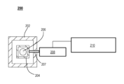
前記前駆体容器の下流かつ前記堆積チャンバの上流のサンプルチャンバであって、水晶マイクロバランス(QCM)デバイスを収容している、サンプルチャンバと;
前記サンプルチャンバ内にヒータと
を含み、
前記水晶マイクロバランス(QCM)デバイスが、ガス冷却チャネルを含み、
前記ヒータ及び前記ガス冷却チャネルが、処理中に前記水晶マイクロバランス(QCM)デバイスを、前記前駆体容器の温度よりも10℃から30℃低い温度で維持するように構成され、
前記サンプルチャンバが、処理中に、前記ヒータによって加熱され、かつ前記前駆体容器の温度よりも10℃から30℃高い範囲の温度を有するように構成される、
処理システム。 - 前記堆積チャンバが、化学気相堆積(CVD)チャンバ又は原子層堆積(ALD)チャンバのうちの1つ又は複数から選択される、請求項1に記載の処理システム。
- 前駆体送達ライン、及び前記サンプルチャンバを前記前駆体送達ラインに接続する三方バルブをさらに含む、請求項1に記載の処理システム。
- 前記サンプルチャンバが、高温バルブ、及び余分な材料の除去を可能にするための、前記高温バルブを有するフォアラインへの流れ経路を含む、請求項1に記載の処理システム。
- 前記キャリアガス源が、アルゴン(Ar)、ヘリウム(He)、キセノン(Xe)、水素(H2)、及び窒素(N2)のうちの1つ又は複数から選択されるキャリアガスを含む、請求項1に記載の処理システム。
- 前記水晶マイクロバランス(QCM)デバイスが、センサヘッド、結晶ホルダ、結晶、フィードスルー、発振器、及び周波数カウンタのうちの1つ又は複数を含む、請求項1に記載の処理システム。
- 前記結晶が、AT結晶又はRC結晶のうちの1つ又は複数を含む、請求項6に記載の処理システム。
- 1から24の範囲の結晶を含む、請求項6に記載の処理システム。
- コントローラをさらに含む、請求項1に記載の処理システム。
- 前記コントローラが、中央処理装置(CPU)、メモリ、回路、及び入力/出力を含む、請求項9に記載の処理システム。
- パージガス源とリザーバとをさらに含み、前記リザーバが、前記前駆体容器及び前記サンプルチャンバの下流にあり、かつ前記堆積チャンバの上流にある、請求項1に記載の処理システム。
- 前記パージガス源が、アルゴン(Ar)、ヘリウム(He)、キセノン(Xe)、水素(H2)、及び窒素(N2)のうちの1つ又は複数から選択されるパージガスを含む、請求項11に記載の処理システム。
- 前記前駆体容器がアンプルである、請求項1に記載の処理システム。
- 前記前駆体容器中の化学前駆体が、固体前駆体又は液体前駆体のうちの1つ又は複数から選択される、請求項1に記載の処理システム。
- 処理システムを用いる処理方法であって、
前記処理システムが、
キャリアガス源と;
前駆体容器と;
堆積チャンバと;
前記前駆体容器の下流かつ前記堆積チャンバの上流のサンプルチャンバであって、水晶マイクロバランス(QCM)デバイスを収容している、サンプルチャンバと;
前記サンプルチャンバ内にヒータと
を含み、
前記水晶マイクロバランス(QCM)デバイスが、ガス冷却チャネルを含み、
前記ヒータ及び前記ガス冷却チャネルが、処理中に前記水晶マイクロバランス(QCM)デバイスを、前記前駆体容器の温度よりも10℃から30℃低い温度で維持するように構成され、
前記処理方法が、
化学前駆体を含有する前記前駆体容器を10℃から600℃の範囲の温度に加熱することであって、前記前駆体容器が第1の前駆体濃度を有する、前記前駆体容器を加熱することと;
前記キャリアガス源からキャリアガスを前記前駆体容器に流して、前記化学前駆体を含む前駆体ガスを形成することと;
前記サンプルチャンバ内の前記水晶マイクロバランス(QCM)デバイスを使用して、前記前駆体ガス中の前記化学前駆体の濃度を測定することであって、前記前駆体ガス中の前記化学前駆体が第2の前駆体濃度を有し、前記サンプルチャンバが、前記ヒータによって加熱され、かつ前記前駆体容器の温度よりも10℃から30℃高い範囲の温度を有する、前記化学前駆体の濃度を測定することと;
堆積プロセス中に基板を前記前駆体ガスに曝露することと;
膜を前記基板上に堆積することと
を含む、処理方法。 - 前記前駆体容器を加熱することが、前記化学前駆体を気化させる、請求項15に記載の処理方法。
- 前記水晶マイクロバランス(QCM)デバイスが、前記前駆体容器の前記温度よりも10℃から15℃低い範囲の温度を有する、請求項15に記載の処理方法。
- 前記前駆体ガス中の前記化学前駆体の前記濃度を前記測定することが、50ミリ秒から20秒の時間フレームで行われる、請求項15に記載の処理方法。
- 命令を含む非一時的なコンピュータ可読媒体であって、前記命令は、処理システムに含まれるコントローラによって実行されると、前記処理システムに動作を実行させ、
前記処理システムが、
キャリアガス源と;
前駆体容器と;
堆積チャンバと;
前記前駆体容器の下流かつ前記堆積チャンバの上流のサンプルチャンバであって、水晶マイクロバランス(QCM)デバイスを収容している、サンプルチャンバと;
前記サンプルチャンバ内にヒータと
をさらに含み、
前記水晶マイクロバランス(QCM)デバイスが、ガス冷却チャネルを含み、
前記ヒータ及び前記ガス冷却チャネルが、処理中に前記水晶マイクロバランス(QCM)デバイスを、前記前駆体容器の温度よりも10℃から30℃低い温度で維持するように構成され、
前記動作が、
化学前駆体を含有する前記前駆体容器を25℃から600℃の範囲の温度に加熱する動作と;
前記キャリアガス源からキャリアガスを前記前駆体容器に流して、前記化学前駆体を含む前駆体ガスを形成する動作と;
前記サンプルチャンバ内の前記水晶マイクロバランス(QCM)デバイスを使用して、前記前駆体ガス中の前記化学前駆体の濃度を測定する動作であって、前記サンプルチャンバが、前記ヒータで加熱され、かつ前記前駆体容器の前記温度よりも10℃から30℃高い範囲の温度を有する、前記化学前駆体の濃度を測定する動作と;
堆積プロセス中に基板を前記前駆体ガスに曝露する動作と;
膜を前記基板上に堆積する動作と
からなる、非一時的コンピュータ可読媒体。 - 前記水晶マイクロバランス(QCM)デバイスが、前記前駆体容器の前記温度よりも10℃から30℃低い範囲の温度を有する、請求項19に記載の非一時的コンピュータ可読媒体。
- 前記前駆体ガス中の前記化学前駆体の前記濃度を前記測定する動作が、100ミリ秒未満の時間フレームで行われる、請求項19に記載の非一時的コンピュータ可読媒体。
Applications Claiming Priority (3)
| Application Number | Priority Date | Filing Date | Title |
|---|---|---|---|
| US16/864,877 US11359286B2 (en) | 2020-05-01 | 2020-05-01 | Quartz crystal microbalance concentration monitor |
| US16/864,877 | 2020-05-01 | ||
| PCT/US2021/030122 WO2021222721A1 (en) | 2020-05-01 | 2021-04-30 | Quartz crystal microbalance concentration monitor |
Publications (2)
| Publication Number | Publication Date |
|---|---|
| JP2023524100A JP2023524100A (ja) | 2023-06-08 |
| JP7702965B2 true JP7702965B2 (ja) | 2025-07-04 |
Family
ID=78292579
Family Applications (1)
| Application Number | Title | Priority Date | Filing Date |
|---|---|---|---|
| JP2022566619A Active JP7702965B2 (ja) | 2020-05-01 | 2021-04-30 | 水晶マイクロバランス濃度モニタ |
Country Status (6)
| Country | Link |
|---|---|
| US (1) | US11359286B2 (ja) |
| JP (1) | JP7702965B2 (ja) |
| KR (1) | KR102919185B1 (ja) |
| CN (1) | CN115698374A (ja) |
| TW (1) | TWI844768B (ja) |
| WO (1) | WO2021222721A1 (ja) |
Families Citing this family (4)
| Publication number | Priority date | Publication date | Assignee | Title |
|---|---|---|---|---|
| WO2022245712A1 (en) * | 2021-05-21 | 2022-11-24 | Applied Materials, Inc. | Consistent known volume liquid metal or metal alloy transfer from atmospheric to vacuum chamber |
| JP2024520494A (ja) * | 2021-06-04 | 2024-05-24 | インフィコン インコーポレイティド | 1つ以上の水晶振動子マイクロバランスセンサを用いた、キャリアストリーム中のプロセスガスの質量流量の測定及び制御のためのシステム及び方法 |
| CN117191924B (zh) * | 2023-08-03 | 2024-04-05 | 哈尔滨工业大学 | 高效分离和动态表征的分子污染物原位分析检测装置 |
| WO2026006337A1 (en) * | 2024-06-27 | 2026-01-02 | Lam Research Corporation | Techniques for thermal management of a precursor delivery line |
Citations (1)
| Publication number | Priority date | Publication date | Assignee | Title |
|---|---|---|---|---|
| WO2019201434A1 (en) | 2018-04-18 | 2019-10-24 | Applied Materials, Inc. | Evaporation source for deposition of evaporated material on a substrate, deposition apparatus, method for measuring a vapor pressure of evaporated material, and method for determining an evaporation rate of an evaporated material |
Family Cites Families (15)
| Publication number | Priority date | Publication date | Assignee | Title |
|---|---|---|---|---|
| JPS62285415A (ja) * | 1986-06-04 | 1987-12-11 | Hitachi Ltd | 気相成長方法及び装置 |
| US6156578A (en) | 1998-06-01 | 2000-12-05 | Advanced Technology Materials, Inc. | Quartz crystal microbalance system for detecting concentration of a selected gas component in a multicomponent gas stream |
| US6295861B1 (en) | 1999-01-28 | 2001-10-02 | Advanced Technology Materials, Inc. | Quartz crystal microbalance sensors and semiconductor manufacturing process systems comprising same |
| US6911092B2 (en) * | 2002-01-17 | 2005-06-28 | Sundew Technologies, Llc | ALD apparatus and method |
| WO2005003406A2 (en) * | 2003-06-27 | 2005-01-13 | Sundew Technologies, Llc | Apparatus and method for chemical source vapor pressure control |
| US20050095859A1 (en) | 2003-11-03 | 2005-05-05 | Applied Materials, Inc. | Precursor delivery system with rate control |
| JP5305393B2 (ja) | 2009-05-22 | 2013-10-02 | 国立大学法人 名古屋工業大学 | 低濃度ガスの検出方法 |
| JP2010285415A (ja) * | 2009-06-15 | 2010-12-24 | Hisamitsu Pharmaceut Co Inc | バレニクリン又は薬学的に許容されるバレニクリン酸付加塩を含有する経皮薬物送達システムの包装体 |
| US8997686B2 (en) * | 2010-09-29 | 2015-04-07 | Mks Instruments, Inc. | System for and method of fast pulse gas delivery |
| US8916021B2 (en) | 2010-10-27 | 2014-12-23 | Applied Materials, Inc. | Electrostatic chuck and showerhead with enhanced thermal properties and methods of making thereof |
| CN103512641B (zh) * | 2013-10-21 | 2016-02-10 | 辽宁新纳斯消防检测有限公司 | 一种用于恒温恒湿箱内质量自动测量系统 |
| DE102015104240A1 (de) * | 2015-03-20 | 2016-09-22 | Aixtron Se | Durch Aufheizen zu reinigender QCM-Sensor und dessen Verwendung in einem OVPD-Beschichtungssystem |
| US10256126B2 (en) | 2016-09-22 | 2019-04-09 | Globalfoundries Inc. | Gas flow process control system and method using crystal microbalance(s) |
| WO2018178036A2 (de) * | 2017-03-31 | 2018-10-04 | Aixtron Se | Verfahren zur bestimmung des partialdrucks oder einer konzentration eines dampfes |
| US11335575B2 (en) | 2017-08-25 | 2022-05-17 | Inficon, Inc. | Unconsumed precursor monitoring |
-
2020
- 2020-05-01 US US16/864,877 patent/US11359286B2/en active Active
-
2021
- 2021-04-08 TW TW110112678A patent/TWI844768B/zh active
- 2021-04-30 KR KR1020227041931A patent/KR102919185B1/ko active Active
- 2021-04-30 JP JP2022566619A patent/JP7702965B2/ja active Active
- 2021-04-30 CN CN202180037573.XA patent/CN115698374A/zh active Pending
- 2021-04-30 WO PCT/US2021/030122 patent/WO2021222721A1/en not_active Ceased
Patent Citations (1)
| Publication number | Priority date | Publication date | Assignee | Title |
|---|---|---|---|---|
| WO2019201434A1 (en) | 2018-04-18 | 2019-10-24 | Applied Materials, Inc. | Evaporation source for deposition of evaporated material on a substrate, deposition apparatus, method for measuring a vapor pressure of evaporated material, and method for determining an evaporation rate of an evaporated material |
Also Published As
| Publication number | Publication date |
|---|---|
| KR20230003198A (ko) | 2023-01-05 |
| JP2023524100A (ja) | 2023-06-08 |
| US20210340674A1 (en) | 2021-11-04 |
| WO2021222721A1 (en) | 2021-11-04 |
| TWI844768B (zh) | 2024-06-11 |
| KR102919185B1 (ko) | 2026-01-27 |
| US11359286B2 (en) | 2022-06-14 |
| CN115698374A (zh) | 2023-02-03 |
| TW202142854A (zh) | 2021-11-16 |
Similar Documents
| Publication | Publication Date | Title |
|---|---|---|
| JP7702965B2 (ja) | 水晶マイクロバランス濃度モニタ | |
| US5282925A (en) | Device and method for accurate etching and removal of thin film | |
| TWI644359B (zh) | 用於低溫原子層沉積膜之腔室底塗層準備方法 | |
| TWI430364B (zh) | 薄膜形成裝置及使用其之方法 | |
| US7625609B2 (en) | Formation of silicon nitride film | |
| US20120183689A1 (en) | Ni film forming method | |
| US9777377B2 (en) | Film forming method and film forming device | |
| US8697578B2 (en) | Film formation apparatus and method for using same | |
| KR101202299B1 (ko) | 반도체 장치의 제조 방법 및 기판 처리 장치 | |
| US20050011445A1 (en) | Apparatus and method for in-situ cleaning of a throttle valve in a CVD system | |
| CN110402477A (zh) | 在氧化硅存在下硅表面上氧化硅或氮化硅的选择性生长 | |
| KR101737215B1 (ko) | 반도체 장치의 제조 방법, 기판 처리 장치 및 프로그램 | |
| KR102946826B1 (ko) | 비정질 탄소 막들의 분자 층 증착 | |
| EP0666339A1 (en) | Method and apparatus for cleaning a throttle valve | |
| TW200937521A (en) | Film formation apparatus for semiconductor process | |
| CN112005343A (zh) | 使用水解的选择性沉积 | |
| KR20010039780A (ko) | 발열체 cvd 장치 및 부착막의 제거방법 | |
| TW202428919A (zh) | 蝕刻或沉積之方法 | |
| JP2004186210A (ja) | 窒素含有ケイ素化合物膜の形成方法 | |
| Li et al. | Copper Film Deposition by Hydrogen Atom Reactions with Copper Compounds | |
| Cui et al. | A thermal processing system for microelectronic materials |
Legal Events
| Date | Code | Title | Description |
|---|---|---|---|
| A621 | Written request for application examination |
Free format text: JAPANESE INTERMEDIATE CODE: A621 Effective date: 20221226 |
|
| A977 | Report on retrieval |
Free format text: JAPANESE INTERMEDIATE CODE: A971007 Effective date: 20240110 |
|
| A131 | Notification of reasons for refusal |
Free format text: JAPANESE INTERMEDIATE CODE: A131 Effective date: 20240220 |
|
| A521 | Request for written amendment filed |
Free format text: JAPANESE INTERMEDIATE CODE: A523 Effective date: 20240517 |
|
| A131 | Notification of reasons for refusal |
Free format text: JAPANESE INTERMEDIATE CODE: A131 Effective date: 20240903 |
|
| A521 | Request for written amendment filed |
Free format text: JAPANESE INTERMEDIATE CODE: A523 Effective date: 20241202 |
|
| A131 | Notification of reasons for refusal |
Free format text: JAPANESE INTERMEDIATE CODE: A131 Effective date: 20250311 |
|
| A521 | Request for written amendment filed |
Free format text: JAPANESE INTERMEDIATE CODE: A523 Effective date: 20250331 |
|
| TRDD | Decision of grant or rejection written | ||
| A01 | Written decision to grant a patent or to grant a registration (utility model) |
Free format text: JAPANESE INTERMEDIATE CODE: A01 Effective date: 20250610 |
|
| A61 | First payment of annual fees (during grant procedure) |
Free format text: JAPANESE INTERMEDIATE CODE: A61 Effective date: 20250624 |
|
| R150 | Certificate of patent or registration of utility model |
Ref document number: 7702965 Country of ref document: JP Free format text: JAPANESE INTERMEDIATE CODE: R150 |