JP7703473B2 - Semiconductor memory device - Google Patents
Semiconductor memory device Download PDFInfo
- Publication number
- JP7703473B2 JP7703473B2 JP2022043340A JP2022043340A JP7703473B2 JP 7703473 B2 JP7703473 B2 JP 7703473B2 JP 2022043340 A JP2022043340 A JP 2022043340A JP 2022043340 A JP2022043340 A JP 2022043340A JP 7703473 B2 JP7703473 B2 JP 7703473B2
- Authority
- JP
- Japan
- Prior art keywords
- data
- read
- unit
- holding unit
- output
- Prior art date
- Legal status (The legal status is an assumption and is not a legal conclusion. Google has not performed a legal analysis and makes no representation as to the accuracy of the status listed.)
- Active
Links
Images


Classifications
-
- G—PHYSICS
- G11—INFORMATION STORAGE
- G11C—STATIC STORES
- G11C7/00—Arrangements for writing information into, or reading information out from, a digital store
- G11C7/10—Input/output [I/O] data interface arrangements, e.g. I/O data control circuits, I/O data buffers
- G11C7/1051—Data output circuits, e.g. read-out amplifiers, data output buffers, data output registers, data output level conversion circuits
- G11C7/1063—Control signal output circuits, e.g. status or busy flags, feedback command signals
-
- G—PHYSICS
- G06—COMPUTING OR CALCULATING; COUNTING
- G06F—ELECTRIC DIGITAL DATA PROCESSING
- G06F12/00—Accessing, addressing or allocating within memory systems or architectures
- G06F12/02—Addressing or allocation; Relocation
- G06F12/0223—User address space allocation, e.g. contiguous or non contiguous base addressing
- G06F12/023—Free address space management
- G06F12/0238—Memory management in non-volatile memory, e.g. resistive RAM or ferroelectric memory
- G06F12/0246—Memory management in non-volatile memory, e.g. resistive RAM or ferroelectric memory in block erasable memory, e.g. flash memory
-
- G—PHYSICS
- G11—INFORMATION STORAGE
- G11C—STATIC STORES
- G11C11/00—Digital stores characterised by the use of particular electric or magnetic storage elements; Storage elements therefor
- G11C11/56—Digital stores characterised by the use of particular electric or magnetic storage elements; Storage elements therefor using storage elements with more than two stable states represented by steps, e.g. of voltage, current, phase, frequency
- G11C11/5621—Digital stores characterised by the use of particular electric or magnetic storage elements; Storage elements therefor using storage elements with more than two stable states represented by steps, e.g. of voltage, current, phase, frequency using charge storage in a floating gate
- G11C11/5642—Sensing or reading circuits; Data output circuits
-
- G—PHYSICS
- G11—INFORMATION STORAGE
- G11C—STATIC STORES
- G11C16/00—Erasable programmable read-only memories
- G11C16/02—Erasable programmable read-only memories electrically programmable
- G11C16/06—Auxiliary circuits, e.g. for writing into memory
- G11C16/08—Address circuits; Decoders; Word-line control circuits
-
- G—PHYSICS
- G11—INFORMATION STORAGE
- G11C—STATIC STORES
- G11C16/00—Erasable programmable read-only memories
- G11C16/02—Erasable programmable read-only memories electrically programmable
- G11C16/06—Auxiliary circuits, e.g. for writing into memory
- G11C16/32—Timing circuits
-
- G—PHYSICS
- G11—INFORMATION STORAGE
- G11C—STATIC STORES
- G11C7/00—Arrangements for writing information into, or reading information out from, a digital store
- G11C7/10—Input/output [I/O] data interface arrangements, e.g. I/O data control circuits, I/O data buffers
- G11C7/1015—Read-write modes for single port memories, i.e. having either a random port or a serial port
- G11C7/1039—Read-write modes for single port memories, i.e. having either a random port or a serial port using pipelining techniques, i.e. using latches between functional memory parts, e.g. row/column decoders, I/O buffers, sense amplifiers
-
- G—PHYSICS
- G11—INFORMATION STORAGE
- G11C—STATIC STORES
- G11C7/00—Arrangements for writing information into, or reading information out from, a digital store
- G11C7/10—Input/output [I/O] data interface arrangements, e.g. I/O data control circuits, I/O data buffers
- G11C7/1051—Data output circuits, e.g. read-out amplifiers, data output buffers, data output registers, data output level conversion circuits
- G11C7/106—Data output latches
-
- G—PHYSICS
- G11—INFORMATION STORAGE
- G11C—STATIC STORES
- G11C7/00—Arrangements for writing information into, or reading information out from, a digital store
- G11C7/10—Input/output [I/O] data interface arrangements, e.g. I/O data control circuits, I/O data buffers
- G11C7/1051—Data output circuits, e.g. read-out amplifiers, data output buffers, data output registers, data output level conversion circuits
- G11C7/1066—Output synchronization
-
- G—PHYSICS
- G11—INFORMATION STORAGE
- G11C—STATIC STORES
- G11C7/00—Arrangements for writing information into, or reading information out from, a digital store
- G11C7/10—Input/output [I/O] data interface arrangements, e.g. I/O data control circuits, I/O data buffers
- G11C7/1051—Data output circuits, e.g. read-out amplifiers, data output buffers, data output registers, data output level conversion circuits
- G11C7/1069—I/O lines read out arrangements
-
- G—PHYSICS
- G11—INFORMATION STORAGE
- G11C—STATIC STORES
- G11C7/00—Arrangements for writing information into, or reading information out from, a digital store
- G11C7/10—Input/output [I/O] data interface arrangements, e.g. I/O data control circuits, I/O data buffers
- G11C7/1078—Data input circuits, e.g. write amplifiers, data input buffers, data input registers, data input level conversion circuits
- G11C7/1096—Write circuits, e.g. I/O line write drivers
-
- G—PHYSICS
- G11—INFORMATION STORAGE
- G11C—STATIC STORES
- G11C7/00—Arrangements for writing information into, or reading information out from, a digital store
- G11C7/22—Read-write [R-W] timing or clocking circuits; Read-write [R-W] control signal generators or management
-
- G—PHYSICS
- G11—INFORMATION STORAGE
- G11C—STATIC STORES
- G11C7/00—Arrangements for writing information into, or reading information out from, a digital store
- G11C7/22—Read-write [R-W] timing or clocking circuits; Read-write [R-W] control signal generators or management
- G11C7/222—Clock generating, synchronizing or distributing circuits within memory device
-
- G—PHYSICS
- G11—INFORMATION STORAGE
- G11C—STATIC STORES
- G11C16/00—Erasable programmable read-only memories
- G11C16/02—Erasable programmable read-only memories electrically programmable
- G11C16/04—Erasable programmable read-only memories electrically programmable using variable threshold transistors, e.g. FAMOS
- G11C16/0483—Erasable programmable read-only memories electrically programmable using variable threshold transistors, e.g. FAMOS comprising cells having several storage transistors connected in series
-
- G—PHYSICS
- G11—INFORMATION STORAGE
- G11C—STATIC STORES
- G11C16/00—Erasable programmable read-only memories
- G11C16/02—Erasable programmable read-only memories electrically programmable
- G11C16/06—Auxiliary circuits, e.g. for writing into memory
- G11C16/26—Sensing or reading circuits; Data output circuits
-
- G—PHYSICS
- G11—INFORMATION STORAGE
- G11C—STATIC STORES
- G11C2207/00—Indexing scheme relating to arrangements for writing information into, or reading information out from, a digital store
- G11C2207/22—Control and timing of internal memory operations
- G11C2207/2272—Latency related aspects
Landscapes
- Engineering & Computer Science (AREA)
- Theoretical Computer Science (AREA)
- Computer Hardware Design (AREA)
- Physics & Mathematics (AREA)
- General Engineering & Computer Science (AREA)
- General Physics & Mathematics (AREA)
- Read Only Memory (AREA)
- Memory System (AREA)
- Techniques For Improving Reliability Of Storages (AREA)
Description
本発明の実施形態は、半導体記憶装置に関する。 An embodiment of the present invention relates to a semiconductor memory device.
例えばNAND型フラッシュメモリのような半導体記憶装置は、メモリコントローラから送信される信号に応じて読み出しデータを出力する。 For example, a semiconductor memory device such as a NAND flash memory outputs read data in response to a signal sent from a memory controller.
開示された実施形態によれば、読み出しデータの出力を安定して行うことのできる半導体記憶装置が提供される。 The disclosed embodiment provides a semiconductor memory device that can stably output read data.
実施形態に係る半導体記憶装置は、データを記憶するメモリセルアレイと、メモリセルアレイから読み出されたデータを一時的に複数保持する保持部と、保持部から繰り返し送信されるデータを外部のメモリコントローラに出力する出力部と、メモリコントローラから、データを読み出すための読み出し信号を繰り返し受信する受信部と、それぞれの読み出し信号に対応して、保持部から出力部へとデータを送信させる制御部と、を備える。制御部は、受信部によって最初に所定回数だけ受信されたそれぞれの読み出し信号に対応するデータとして、メモリコントローラが要求するデータとは異なる非正規データを、保持部から出力部へと送信させ、受信部によってその後に受信された読み出し信号に対応するデータとして、メモリコントローラが要求するデータである正規データを、保持部から出力部へと送信させるものである。制御部は、保持部に保持されている複数のデータのうち、出力部に向けて次に送信されるデータ、の保持位置を示すリードポインタを、所定回数に応じて予め調整しておくことで、保持部から非正規データを送信させる。 The semiconductor memory device according to the embodiment includes a memory cell array for storing data, a holding unit for temporarily holding multiple pieces of data read from the memory cell array, an output unit for outputting data repeatedly transmitted from the holding unit to an external memory controller, a receiving unit for repeatedly receiving a read signal for reading data from the memory controller, and a control unit for causing the holding unit to transmit data to the output unit in response to each read signal. The control unit causes the holding unit to transmit non-regular data different from the data requested by the memory controller as data corresponding to each read signal first received a predetermined number of times by the receiving unit to the output unit, and causes the holding unit to transmit regular data, which is the data requested by the memory controller as data corresponding to a read signal subsequently received by the receiving unit, to the output unit. The control unit causes the holding unit to transmit the non-regular data by adjusting in advance a read pointer indicating the holding position of the data to be next transmitted to the output unit among the multiple pieces of data held in the holding unit according to the predetermined number of times.
以下、添付図面を参照しながら本実施形態について説明する。説明の理解を容易にするため、各図面において同一の構成要素に対しては可能な限り同一の符号を付して、重複する説明は省略する。 The present embodiment will be described below with reference to the attached drawings. To facilitate understanding of the description, the same components in each drawing are denoted by the same reference numerals as much as possible, and duplicate descriptions will be omitted.
本実施形態に係る半導体記憶装置2は、NAND型フラッシュメモリとして構成された不揮発性の記憶装置である。図1には、半導体記憶装置2を含むメモリシステムの構成例がブロック図として示されている。このメモリシステムは、メモリコントローラ1と、半導体記憶装置2とを備える。
The
尚、実際のメモリシステムにおいては、図2に示されるように、1つのメモリコントローラ1に対し複数の半導体記憶装置2が設けられている。図1においては、複数ある半導体記憶装置2のうちの1つのみが図示されている。半導体記憶装置2の具体的な構成については後に説明する。
In an actual memory system, as shown in FIG. 2, multiple
このメモリシステムは、不図示のホストと接続可能である。ホストは、例えば、パーソナルコンピュータや携帯端末等の電子機器である。メモリコントローラ1は、ホストからの書き込みリクエストに従って半導体記憶装置2へのデータの書き込みを制御する。また、メモリコントローラ1は、ホストからの読み出しリクエストに従って半導体記憶装置2からのデータの読み出しを制御する。
This memory system can be connected to a host (not shown). The host is, for example, an electronic device such as a personal computer or a mobile terminal. The
メモリコントローラ1と半導体記憶装置2との間では、チップイネーブル信号/CE、レディービジー信号R/B、コマンドラッチイネーブル信号CLE、アドレスラッチイネーブル信号ALE、ライトイネーブル信号/WE、リードイネーブル信号/RE、RE、ライトプロテクト信号/WP、データである信号DQ<7:0>、データストローブ信号DQS、/DQS、の各信号が送受信される。
The following signals are transmitted and received between the
チップイネーブル信号/CEは、半導体記憶装置2をイネーブルにするための信号である。レディービジー信号R/Bは、半導体記憶装置2がレディ状態であるか、ビジー状態であるかを示すための信号である。「レディ状態」とは、外部からの命令を受け付ける状態である。「ビジー状態」とは、外部からの命令を受け付けない状態である。
The chip enable signal /CE is a signal for enabling the
図2に示されるように、複数の半導体記憶装置2のそれぞれには、チップイネーブル信号/CEが個別に送信される。図2においては、それぞれのチップイネーブル信号/CEを互いに区別し得るよう、、例えば「/CE0」のように末尾に番号が付してある。
As shown in FIG. 2, a chip enable signal /CE is sent individually to each of the multiple
同様に、複数の半導体記憶装置2のそれぞれからは、レディービジー信号R/Bが個別に送信される。図2においては、それぞれのレディービジー信号R/Bを互いに区別し得るよう、例えば「R/B0」のように末尾に番号が付してある。
Similarly, a ready/busy signal R/B is transmitted individually from each of the multiple
チップイネーブル信号/CEやレディービジー信号R/B以外の信号(コマンドラッチイネーブル信号CLE等)については、複数の半導体記憶装置2で共通となっている信号線を介して、メモリコントローラ1と半導体記憶装置2との間で送受信される。メモリコントローラ1は、個別のチップイネーブル信号/CEを用いて、通信の対象となる半導体記憶装置2を特定する。
Signals other than the chip enable signal /CE and the ready/busy signal R/B (such as the command latch enable signal CLE) are transmitted and received between the
コマンドラッチイネーブル信号CLEは、信号DQ<7:0>がコマンドであることを示す信号である。アドレスラッチイネーブル信号ALEは、信号DQ<7:0>がアドレスであることを示す信号である。ライトイネーブル信号/WEは、受信した信号を半導体記憶装置2に取り込むための信号であり、メモリコントローラ1によりコマンド、アドレス、及びデータを受信する都度アサートされる。メモリコントローラ1は、信号/WEが“L(Low)”レベルである間に信号DQ<7:0>を取り込むよう半導体記憶装置2に指示する。
The command latch enable signal CLE is a signal indicating that the signal DQ<7:0> is a command. The address latch enable signal ALE is a signal indicating that the signal DQ<7:0> is an address. The write enable signal /WE is a signal for loading the received signal into the
リードイネーブル信号/REは、メモリコントローラ1が、半導体記憶装置2からデータを読み出すための信号である。信号REは信号/REの相補信号である。これらは例えば、信号DQ<7:0>を出力する際の半導体記憶装置2の動作タイミングを制御するために使用される。ライトプロテクト信号/WPは、データ書き込み及び消去の禁止を半導体記憶装置2に指示するための信号である。信号DQ<7:0>は、半導体記憶装置2とメモリコントローラ1との間で送受信されるデータの実体であり、コマンド、アドレス、及びデータを含む。データストローブ信号DQSは、信号DQ<7:0>の入出力のタイミングを制御するための信号である。信号/DQSは信号DQSの相補信号である。
The read enable signal /RE is a signal that causes the
メモリコントローラ1は、RAM11と、プロセッサ12と、ホストインターフェイス13と、ECC回路14と、メモリインターフェイス15と、を備える。RAM11、プロセッサ12、ホストインターフェイス13、ECC回路14、及びメモリインターフェイス15は、互いに内部バス16で接続されている。
The
ホストインターフェイス13は、ホストから受信したリクエスト、ユーザデータ(書き込みデータ)等を内部バス16に出力する。また、ホストインターフェイス13は、半導体記憶装置2から読み出されたユーザデータ、プロセッサ12からの応答等をホストへ送信する。
The
メモリインターフェイス15は、プロセッサ12の指示に基づいて、ユーザデータ等を半導体記憶装置2へ書き込む処理、及び、半導体記憶装置2から読み出す処理を制御する。
The
プロセッサ12は、メモリコントローラ1を統括的に制御する。プロセッサ12は、例えばCPUやMPU等である。プロセッサ12は、ホストからホストインターフェイス13経由でリクエストを受けた場合に、そのリクエストに従った制御を行う。例えば、プロセッサ12は、ホストからのリクエストに従って、半導体記憶装置2へのユーザデータ及びパリティの書き込みをメモリインターフェイス15へ指示する。また、プロセッサ12は、ホストからのリクエストに従って、半導体記憶装置2からのユーザデータ及びパリティの読み出しをメモリインターフェイス15へ指示する。
The
プロセッサ12は、RAM11に蓄積されるユーザデータに対して、半導体記憶装置2上の格納領域(メモリ領域)を決定する。ユーザデータは、内部バス16経由でRAM11に格納される。プロセッサ12は、メモリ領域の決定を、書き込み単位であるページ単位のデータ(ページデータ)に対して実施する。半導体記憶装置2の1ページに格納されるユーザデータのことを、以下では「ユニットデータ」とも称する。ユニットデータは、一般的には符号化されて、符号語として半導体記憶装置2に格納される。本実施形態では、符号化は必須ではない。メモリコントローラ1は、符号化せずにユニットデータを半導体記憶装置2に格納してもよいが、図1では、一構成例として符号化を行う構成を示している。メモリコントローラ1が符号化を行わない場合には、ページデータはユニットデータと一致する。また、1つのユニットデータに基づいて1つの符号語が生成されてもよいし、ユニットデータが分割された分割データに基づいて1つの符号語が生成されてもよい。また、複数のユニットデータを用いて1つの符号語が生成されてもよい。
The
プロセッサ12は、ユニットデータごとに書き込み先の半導体記憶装置2のメモリ領域を決定する。半導体記憶装置2のメモリ領域には物理アドレスが割当てられている。プロセッサ12は、ユニットデータの書き込み先のメモリ領域を、物理アドレスを用いて管理する。プロセッサ12は、決定したメモリ領域(物理アドレス)を指定してユーザデータを半導体記憶装置2へ書き込むようメモリインターフェイス15へ指示する。プロセッサ12は、ユーザデータの論理アドレス(ホストが管理する論理アドレス)と物理アドレスとの対応を管理する。プロセッサ12は、ホストからの論理アドレスを含む読み出しリクエストを受信した場合は、論理アドレスに対応する物理アドレスを特定し、物理アドレスを指定してユーザデータの読み出しをメモリインターフェイス15へ指示する。
The
ECC回路14は、RAM11に格納されたユーザデータを符号化して、符号語を生成する。また、ECC回路14は、半導体記憶装置2から読み出された符号語を復号する。ECC回路14は、例えばユーザデータに付与されたチェックサム等を利用することで、データにおけるエラーの検出、及び当該エラーの訂正を行う。
The
RAM11は、ホストから受信したユーザデータを半導体記憶装置2へ記憶するまでに一時格納したり、半導体記憶装置2から読み出したデータをホストへ送信するまでに一時格納したりする。RAM11は、例えば、SRAMやDRAM等の汎用メモリである。
図1では、メモリコントローラ1が、ECC回路14とメモリインターフェイス15をそれぞれ備える構成例が示されている。しかしながら、ECC回路14がメモリインターフェイス15に内蔵されていてもよい。また、ECC回路14が、半導体記憶装置2に内蔵されていてもよい。図1に示される各要素の具体的な構成や配置は、特に限定されない。
In FIG. 1, a configuration example is shown in which the
ホストから書き込みリクエストを受信した場合、図1のメモリシステムは次のように動作する。プロセッサ12は、書き込み動作の対象となるデータをRAM11に一時記憶させる。プロセッサ12は、RAM11にストアされたデータを読み出し、ECC回路14に入力する。ECC回路14は、入力されたデータを符号化し、符号語をメモリインターフェイス15に入力する。メモリインターフェイス15は、入力された符号語を半導体記憶装置2に書き込む。
When a write request is received from the host, the memory system in FIG. 1 operates as follows. The
ホストから読み出しリクエストを受信した場合、図1のメモリシステムは次のように動作する。メモリインターフェイス15は、半導体記憶装置2から読み出した符号語をECC回路14に入力する。ECC回路14は、入力された符号語を復号し、復号されたデータをRAM11にストアする。プロセッサ12は、RAM11にストアされたデータを、ホストインターフェイス13を介してホストに送信する。
When a read request is received from the host, the memory system in FIG. 1 operates as follows. The
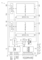
半導体記憶装置2の構成について説明する。図3に示されるように、半導体記憶装置2は、2つのプレーンPL1、PL2と、入出力回路21と、ロジック制御回路22と、シーケンサ41と、レジスタ42と、電圧生成回路43と、入出力用パッド群31と、ロジック制御用パッド群32と、電源入力用端子群33と、を備えている。
The configuration of the
プレーンPL1は、メモリセルアレイ110と、センスアンプ120と、ロウデコーダ130と、を備えている。また、プレーンPL2は、メモリセルアレイ210と、センスアンプ220と、ロウデコーダ230と、を備えている。プレーンPL1の構成とプレーンPL2の構成とは互いに同一である。つまり、メモリセルアレイ110の構成とメモリセルアレイ210の構成とは互いに同一であり、センスアンプ120の構成とセンスアンプ220の構成とは互いに同一であり、ロウデコーダ130の構成とロウデコーダ230の構成とは互いに同一である。半導体記憶装置2に設けられているプレーンの数は、本実施形態のように2つであってもよいが、1つでもよく、3つ以上であってもよい。
Plane PL1 includes a
メモリセルアレイ110及びメモリセルアレイ210は、データを記憶する部分である。メモリセルアレイ110及びメモリセルアレイ210のそれぞれは、ワード線及びビット線に関連付けられた複数のメモリセルトランジスタを含んでいる。これらの具体的な構成については後に説明する。
入出力回路21は、メモリコントローラ1との間で、信号DQ<7:0>、及び、データストローブ信号DQS、/DQSを送受信する。入出力回路21は、信号DQ<7:0>内のコマンド及びアドレスをレジスタ42に転送する。また、入出力回路21は、書き込みデータ及び読み出しデータを、センスアンプ120やセンスアンプ220との間で送受信する。入出力回路21は、メモリコントローラ1からのコマンド等を受信する「入力回路」としての機能と、メモリコントローラ1にデータを出力する「出力回路」としての機能と、の両方を有している。このような態様に換えて、入力回路と出力回路とが互いに別の回路として構成されている態様としてもよい。
The input/
ロジック制御回路22は、メモリコントローラ1からチップイネーブル信号/CE、コマンドラッチイネーブル信号CLE、アドレスラッチイネーブル信号ALE、ライトイネーブル信号/WE、リードイネーブル信号RE、/RE、及びライトプロテクト信号/WPを受信する。また、ロジック制御回路22は、レディービジー信号R/Bをメモリコントローラ1に転送して、半導体記憶装置2の状態を外部に通知する。
The
入出力回路21及びロジック制御回路22は、いずれも、メモリコントローラ1との間で信号が入出力される部分として構成された回路である。つまり、入出力回路21及びロジック制御回路22は、半導体記憶装置2のインターフェイス回路として設けられている。
The input/
シーケンサ41は、メモリコントローラ1から半導体記憶装置2へと入力された制御信号に基づいて、プレーンPL1、PL2や電圧生成回路43等の各部の動作を制御する。シーケンサ41は、メモリセルアレイ110、210等の動作を制御する部分であり、半導体記憶装置2の「制御部」に該当する。シーケンサ41とロジック制御回路22の両方を上記の「制御部」と見なすこともできる。
The
レジスタ42は、コマンドやアドレスを一時的に保持する部分である。レジスタ42は、プレーンPL1、PL2のそれぞれの状態を示すステータス情報をも保持する部分となっている。ステータス情報は、メモリコントローラ1からの要求に応じて、状態信号として入出力回路21からメモリコントローラ1へと出力される。
電圧生成回路43は、シーケンサ41からの指示に基づき、メモリセルアレイ110、210におけるデータの書き込み動作、読み出し動作、及び、消去動作のそれぞれに必要な電圧を生成する部分である。このような電圧には、例えば、後述のワード線WLに対し印加されるVPGMやVPASS_PGM、VPASS_READのような電圧や、後述のビット線BLに印加される電圧等が含まれる。電圧生成回路43は、プレーンPL1及びプレーンPL2が互いに並列動作し得るように、各ワード線WLやビット線BL等のそれぞれに対し個別に電圧を印加することが可能となっている。
The
入出力用パッド群31は、メモリコントローラ1と入出力回路21との間で各信号の送受信を行うための、複数の端子(パッド)が設けられた部分である。それぞれの端子は、信号DQ<7:0>、及び、データストローブ信号DQS、/DQSのそれぞれに対応して個別に設けられている。
The input/
ロジック制御用パッド群32は、メモリコントローラ1とロジック制御回路22との間で各信号の送受信を行うための、複数の端子(パッド)が設けられた部分である。それぞれの端子は、チップイネーブル信号/CE、コマンドラッチイネーブル信号CLE、アドレスラッチイネーブル信号ALE、ライトイネーブル信号/WE、リードイネーブル信号RE、/RE、ライトプロテクト信号/WP、及び、レディービジー信号R/Bのそれぞれに対応して個別に設けられている。
The logic
電源入力用端子群33は、半導体記憶装置2の動作に必要な各電圧の印加を受けるための、複数の端子が設けられた部分である。それぞれの端子に印加される電圧には、電源電圧Vcc、VccQ、Vpp、及び接地電圧Vssが含まれる。
The power
電源電圧Vccは、動作電源として外部から与えられる回路電源電圧であり、例えば3.3V程度の電圧である。電源電圧VccQは、例えば1.2Vの電圧である。電源電圧VccQは、メモリコントローラ1と半導体記憶装置2との間で信号を送受信する際に用いられる電圧である。電源電圧Vppは、電源電圧Vccよりも高圧の電源電圧であり、例えば12Vの電圧である。
The power supply voltage Vcc is a circuit power supply voltage provided from the outside as an operating power supply, and is, for example, a voltage of about 3.3 V. The power supply voltage VccQ is, for example, a voltage of 1.2 V. The power supply voltage VccQ is a voltage used when transmitting and receiving signals between the
メモリセルアレイ110、210へデータを書き込んだり、データを消去したりする際には、20V程度の高い電圧(VPGM)が必要となる。この際に、約3.3Vの電源電圧Vccを電圧生成回路43の昇圧回路で昇圧するよりも、約12Vの電源電圧Vppを昇圧するほうが、高速かつ低消費電力で所望の電圧を生成することができる。一方で、例えば、高電圧を供給することができない環境において半導体記憶装置2が用いられる場合、電源電圧Vppには電圧が供給されなくともよい。電源電圧Vppが供給されない場合であっても、半導体記憶装置2は、電源電圧Vccが供給されていれば、各種の動作を実行することができる。すなわち、電源電圧Vccは、半導体記憶装置2に標準的に供給される電源であり、電源電圧Vppは、例えば使用環境に応じて追加的・任意的に供給される電源である。
When writing data to the
プレーンPL1、PL2の構成について説明する。尚、先に述べたように、プレーンPL1の構成とプレーンPL2の構成とは互いに同一である。このため、以下ではプレーンPL1の構成についてのみ説明し、プレーンPL2の構成については図示及び説明を省略する。 The configuration of planes PL1 and PL2 will be described. As mentioned above, the configuration of plane PL1 and the configuration of plane PL2 are identical to each other. For this reason, only the configuration of plane PL1 will be described below, and illustrations and explanations of the configuration of plane PL2 will be omitted.
図4には、プレーンPL1に設けられたメモリセルアレイ110の構成が、等価回路図として示されている。メモリセルアレイ110は複数のブロックBLKにより構成されているのであるが、図4においては、これらのうちの1つのブロックBLKのみが図示されている。メモリセルアレイ110が有する他のブロックBLKの構成も、図4に示されるものと同じである。
Figure 4 shows the configuration of the
図4に示されるように、ブロックBLKは、例えば4つのストリングユニットSU(SU0~SU3)を含む。また各々のストリングユニットSUは、複数のNANDストリングNSを含む。NANDストリングNSの各々は、例えば8個のメモリセルトランジスタMT(MT0~MT7)と、選択トランジスタST1、ST2とを含む。 As shown in FIG. 4, the block BLK includes, for example, four string units SU (SU0 to SU3). Each string unit SU includes a plurality of NAND strings NS. Each of the NAND strings NS includes, for example, eight memory cell transistors MT (MT0 to MT7) and select transistors ST1 and ST2.
尚、メモリセルトランジスタMTの個数は8個に限られず、例えば、32個、48個、64個、96個でもよい。例えばカットオフ特性を高めるために、選択トランジスタST1、ST2のそれぞれが、単一ではなく複数のトランジスタにより構成されていてもよい。さらに、メモリセルトランジスタMTと選択トランジスタST1、ST2との間には、ダミーセルトランジスタが設けられていてもよい。 The number of memory cell transistors MT is not limited to eight, and may be, for example, 32, 48, 64, or 96. For example, in order to improve the cutoff characteristics, each of the select transistors ST1 and ST2 may be composed of multiple transistors rather than a single one. Furthermore, dummy cell transistors may be provided between the memory cell transistors MT and the select transistors ST1 and ST2.
メモリセルトランジスタMTは、選択トランジスタST1と選択トランジスタST2との間において、直列接続されるようにして配置されている。一端側のメモリセルトランジスタMT7が、選択トランジスタST1のソースに接続され、他端側のメモリセルトランジスタMT0が、選択トランジスタST2のドレインに接続されている。 The memory cell transistors MT are arranged between the select transistors ST1 and ST2 so that they are connected in series. The memory cell transistor MT7 on one end is connected to the source of the select transistor ST1, and the memory cell transistor MT0 on the other end is connected to the drain of the select transistor ST2.
ストリングユニットSU0~SU3の各々の選択トランジスタST1のゲートは、それぞれセレクトゲート線SGD0~SGD3に共通接続されている。選択トランジスタST2のゲートは、同一のブロックBLK内にある複数のストリングユニットSU間で同一のセレクトゲート線SGSに共通接続されている。同一のブロックBLK内にあるメモリセルトランジスタMT0~MT7のゲートは、それぞれワード線WL0~WL7に共通接続される。すなわち、ワード線WL0~WL7及びセレクトゲート線SGSは、同一ブロックBLK内の複数のストリングユニットSU0~SU3間で共通となっているのに対し、セレクトゲート線SGDは、同一ブロックBLK内であってもストリングユニットSU0~SU3毎に個別に設けられている。 The gates of the select transistors ST1 of the string units SU0 to SU3 are commonly connected to the select gate lines SGD0 to SGD3, respectively. The gates of the select transistors ST2 are commonly connected to the same select gate line SGS between multiple string units SU in the same block BLK. The gates of the memory cell transistors MT0 to MT7 in the same block BLK are commonly connected to the word lines WL0 to WL7, respectively. In other words, the word lines WL0 to WL7 and the select gate line SGS are common to multiple string units SU0 to SU3 in the same block BLK, while the select gate line SGD is provided individually for each string unit SU0 to SU3 even within the same block BLK.
メモリセルアレイ110には、m本のビット線BL(BL0、BL1、・・・、BL(m-1))が設けられている。上記の「m」は、1つのストリングユニットSUに含まれるNANDストリングNSの本数を表す整数である。それぞれのNANDストリングNSのうち、選択トランジスタST1のドレインは、対応するビット線BLに接続されている。選択トランジスタST2のソースは、ソース線SLに接続されている。ソース線SLは、ブロックBLKが有する複数の選択トランジスタST2のソースに対し、共通接続されている。
The
同一のブロックBLK内にある複数のメモリセルトランジスタMTに記憶されているデータは、一括して消去される。一方、データの読み出し及び書き込みは、1つのワード線WLに接続され、かつ1つのストリングユニットSUに属する複数のメモリセルトランジスタMTに対して一括して行われる。それぞれのメモリセルは、上位ビット、中位ビット、及び下位ビットからなる3ビットのデータを保持することができる。 Data stored in multiple memory cell transistors MT in the same block BLK is erased all at once. On the other hand, data is read and written all at once to multiple memory cell transistors MT connected to one word line WL and belonging to one string unit SU. Each memory cell can hold three bits of data consisting of an upper bit, a middle bit, and a lower bit.
つまり、本実施形態に係る半導体記憶装置2は、メモリセルトランジスタMTへのデータの書き込み方式として、1つのメモリセルトランジスタMTに3ビットデータを記憶させるTLC方式を採用している。このような態様に換えて、メモリセルトランジスタMTへのデータの書き込み方式としては、1つのメモリセルトランジスタMTに2ビットデータを記憶させるMLC方式等を採用してもよい。1つのメモリセルトランジスタMTに記憶されるデータのビット数は特に限定されない。
In other words, the
尚、以下の説明では、1つのワード線WLに接続され、かつ1つのストリングユニットSUに属する複数のメモリセルトランジスタMTが記憶する1ビットデータの集合のことを「ページ」と称する。図4では、上記のような複数のメモリセルトランジスタMTからなる集合の一つに、符号「MG」が付してある。 In the following description, a set of 1-bit data stored in multiple memory cell transistors MT connected to one word line WL and belonging to one string unit SU is referred to as a "page." In FIG. 4, one of the sets of multiple memory cell transistors MT as described above is marked with the symbol "MG."
本実施形態のように、1つのメモリセルトランジスタMTに3ビットのデータが記憶される場合、1つのストリングユニットSU内で共通のワード線WLに接続された複数のメモリセルトランジスタMTの集合は、3ページ分のデータを記憶することができる。これらのうち、下位ビットデータの集合からなるページのことを以下では「下位ページ」とも称し、下位ページのデータのことを以下では「下位ページデータ」とも称する。同様に、中位ビットデータの集合からなるページのことを以下では「中位ページ」とも称し、中位ページのデータのことを以下では「中位ページデータ」とも称する。上位ビットデータの集合からなるページのことを以下では「上位ページ」とも称し、上位ページのデータのことを以下では「上位ページデータ」とも称する。 When three bits of data are stored in one memory cell transistor MT as in this embodiment, a set of multiple memory cell transistors MT connected to a common word line WL in one string unit SU can store three pages of data. Of these, a page consisting of a set of lower bit data is also referred to as a "lower page" below, and the data of the lower page is also referred to as "lower page data" below. Similarly, a page consisting of a set of middle bit data is also referred to as a "middle page" below, and the data of the middle page is also referred to as "middle page data" below. A page consisting of a set of upper bit data is also referred to as an "upper page" below, and the data of the upper page is also referred to as "upper page data" below.
図5には、メモリセルアレイ110及びその周辺の構成が、模式的な断面図として示されている。同図に示されるように、メモリセルアレイ110では、導電体層320の上に複数のNANDストリングNSが形成されている。導電体層320は、埋め込みソース線(BSL)とも称されるものであり、図4のソース線SLに該当するものである。
FIG. 5 shows a schematic cross-sectional view of the
導電体層320の上方には、セレクトゲート線SGSとして機能する複数の配線層333、ワード線WLとして機能する複数の配線層332、及びセレクトゲート線SGDとして機能する複数の配線層331が積層されている。積層された配線層333、332、331のそれぞれの間には、不図示の絶縁層が配置されている。
Above the
メモリセルアレイ110には複数のメモリホール334が形成されている。メモリホール334は、上記の配線層333、332、331、及びこれらの間にある不図示の絶縁層を上下方向に貫通しており、且つ導電体層320に達する穴である。メモリホール334の側面には、ブロック絶縁膜335、電荷蓄積層336、及びゲート絶縁膜337が順次形成され、更にその内側に導電体柱338が埋め込まれている。導電体柱338は、例えばポリシリコンからなり、NANDストリングNSに含まれるメモリセルトランジスタMT並びに選択トランジスタST1及びST2の動作時にチャネルが形成される領域として機能する。このように、メモリホール334の内側には、ブロック絶縁膜335、電荷蓄積層336、ゲート絶縁膜337、及び導電体柱338からなる柱状体が形成されている。
A plurality of
メモリホール334の内側に形成された柱状体のうち、積層された配線層333、332、331のそれぞれと交差している各部分は、トランジスタとして機能する。これら複数のトランジスタのうち、配線層331と交差している部分にあるものは、選択トランジスタST1として機能する。複数のトランジスタのうち、配線層332と交差している部分にあるものは、メモリセルトランジスタMT(MT0~MT7)として機能する。複数のトランジスタのうち、配線層333と交差している部分にあるものは、選択トランジスタST2として機能する。このような構成により、各メモリホール334の内側に形成された柱状体のそれぞれは、図4を参照しながら説明したNANDストリングNSとして機能する。柱状体の内側にある導電体柱338は、メモリセルトランジスタMTや選択トランジスタST1、ST2のチャンネルとして機能する部分である。
Of the pillars formed inside the
導電体柱338よりも上側には、ビット線BLとして機能する配線層が形成される。導電体柱338の上端には、導電体柱338とビット線BLとを接続するコンタクトプラグ339が形成されている。
A wiring layer that functions as a bit line BL is formed above the
図5に示される構成と同様の構成が、図5の紙面の奥行き方向に沿って複数配列されている。図5の紙面の奥行き方向に沿って一列に並ぶ複数のNANDストリングNSの集合によって、1つのストリングユニットSUが形成されている。 Multiple configurations similar to the configuration shown in FIG. 5 are arranged in a row along the depth direction of the paper of FIG. 5. A single string unit SU is formed by a collection of multiple NAND strings NS aligned in a row along the depth direction of the paper of FIG. 5.
本実施形態に係る半導体記憶装置2では、メモリセルアレイ110の下方側、すなわち、メモリセルアレイ110と半導体基板300との間となる位置に、周辺回路PERが設けられている。周辺回路PERは、メモリセルアレイ110におけるデータの書き込み動作や読み出し動作、及び消去動作等を実現するために設けられた回路である。図3に示されるセンスアンプ120、ロウデコーダ130、及び電圧生成回路43等は、周辺回路PERの一部となっている。周辺回路PERは、各種のトランジスタやRC回路等を含んでいる。図5に示される例では、半導体基板300上に形成されたトランジスタTRと、メモリセルアレイ110の上方側にあるビット線BLとの間が、コンタクト924を介して電気的に接続されている。
In the
尚、このような構成に換えて、半導体基板300の上に直接メモリセルアレイ110が設けられている構成としてもよい。この場合、半導体基板300のp型ウェル領域が、ソース線SLとして機能することとなる。また、周辺回路PERは、半導体基板300の表面に沿ってメモリセルアレイ110と隣り合う位置に設けられることとなる。
Instead of this configuration, the
図3に戻って説明を続ける。先に述べたように、プレーンPL1には、上記のメモリセルアレイ110に加えて、センスアンプ120とロウデコーダ130とが設けられている。
Returning to FIG. 3, the explanation continues. As mentioned above, in addition to the
センスアンプ120は、ビット線BLに印加される電圧を調整したり、ビット線BLの電圧を読み出してデータに変換したりするための回路である。センスアンプ120は、データの読み出し時には、メモリセルトランジスタMTからビット線BLに読み出された読み出しデータを取得し、取得した読み出しデータを入出力回路21に転送する。センスアンプ120は、データの書き込み時には、ビット線BLを介して書き込まれる書き込みデータをメモリセルトランジスタMTに転送する。
The
ロウデコーダ130は、ワード線WLのそれぞれに電圧を印加するための、不図示のスイッチ群として構成された回路である。ロウデコーダ130は、レジスタ42からブロックアドレス及びロウアドレスを受け取り、当該ブロックアドレスに基づいて対応するブロックBLKを選択するとともに、当該ロウアドレスに基づいて対応するワード線WLを選択する。ロウデコーダ130は、選択されたワード線WLに対して電圧生成回路43からの電圧が印加されるよう、上記のスイッチ群の開閉を切り換える。
The
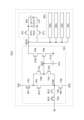
図6には、センスアンプ120の構成例が示されている。センスアンプ120は、複数のビット線BLのそれぞれに関連付けられた複数のセンスアンプユニットSAUを含む。図6には、これらのうちの1つのセンスアンプユニットSAUの詳細な回路構成が抽出して示されている。
Figure 6 shows an example of the configuration of the
図6に示されるように、センスアンプユニットSAUは、センスアンプ部SAと、ラッチ回路SDL、ADL、BDL、CDL、XDLとを含んでいる。センスアンプ部SA、ラッチ回路SDL、ADL、BDL、CDL、XDLは、互いにデータを送受信可能なように、バスLBUSによって接続されている。 As shown in FIG. 6, the sense amplifier unit SAU includes a sense amplifier section SA and latch circuits SDL, ADL, BDL, CDL, and XDL. The sense amplifier section SA and the latch circuits SDL, ADL, BDL, CDL, and XDL are connected by a bus LBUS so that they can transmit and receive data to and from each other.
センスアンプ部SAは、例えば読み出し動作において、対応するビット線BLに読み出されたデータをセンスして、読み出したデータが“0”であるか“1”であるかを判定する。センスアンプ部SAは、例えば、pチャネルMOSトランジスタであるトランジスタTR1と、nチャネルMOSトランジスタであるトランジスタTR2~TR9と、キャパシタC10とを含んでいる。 For example, in a read operation, the sense amplifier unit SA senses the data read to the corresponding bit line BL and determines whether the read data is "0" or "1". The sense amplifier unit SA includes, for example, a p-channel MOS transistor TR1, n-channel MOS transistors TR2 to TR9, and a capacitor C10.
トランジスタTR1の一端は電源線に接続されており、トランジスタTR1の他端はトランジスタTR2に接続されている。トランジスタTR1のゲートは、ラッチ回路SDL内のノードINVに接続されている。トランジスタTR2の一端はトランジスタTR1に接続されており、トランジスタTR2の他端はノードCOMに接続されている。トランジスタTR2のゲートには信号BLXが入力される。トランジスタTR3の一端はノードCOMに接続されており、トランジスタTR3の他端はトランジスタTR4に接続されている。トランジスタTR3のゲートには信号BLCが入力される。トランジスタTR4は、高耐圧のMOSトランジスタである。トランジスタTR4の一端はトランジスタTR3に接続されている。トランジスタTR4の他端は対応するビット線BLに接続されている。トランジスタTR4のゲートには信号BLSが入力される。 One end of transistor TR1 is connected to the power supply line, and the other end of transistor TR1 is connected to transistor TR2. The gate of transistor TR1 is connected to node INV in latch circuit SDL. One end of transistor TR2 is connected to transistor TR1, and the other end of transistor TR2 is connected to node COM. A signal BLX is input to the gate of transistor TR2. One end of transistor TR3 is connected to node COM, and the other end of transistor TR3 is connected to transistor TR4. A signal BLC is input to the gate of transistor TR3. Transistor TR4 is a high-voltage MOS transistor. One end of transistor TR4 is connected to transistor TR3. The other end of transistor TR4 is connected to the corresponding bit line BL. A signal BLS is input to the gate of transistor TR4.
トランジスタTR5の一端はノードCOMに接続されており、トランジスタTR5の他端はノードSRCに接続されている。トランジスタTR5のゲートはノードINVに接続されている。トランジスタTR6の一端は、トランジスタTR1とトランジスタTR2との間に接続されており、トランジスタTR6の他端はノードSENに接続されている。トランジスタTR6のゲートには信号HLLが入力される。トランジスタTR7の一端はノードSENに接続されており、トランジスタTR7の他端はノードCOMに接続されている。トランジスタTR7のゲートには信号XXLが入力される。 One end of transistor TR5 is connected to node COM, and the other end of transistor TR5 is connected to node SRC. The gate of transistor TR5 is connected to node INV. One end of transistor TR6 is connected between transistor TR1 and transistor TR2, and the other end of transistor TR6 is connected to node SEN. A signal HLL is input to the gate of transistor TR6. One end of transistor TR7 is connected to node SEN, and the other end of transistor TR7 is connected to node COM. A signal XXL is input to the gate of transistor TR7.
トランジスタTR8の一端は接地されており、トランジスタTR8の他端はトランジスタTR9に接続されている。トランジスタTR8のゲートはノードSENに接続されている。トランジスタTR9の一端はトランジスタTR8に接続されており、トランジスタTR9の他端はバスLBUSに接続されている。トランジスタTR9のゲートには信号STBが入力される。キャパシタC10の一端はノードSENに接続されている。キャパシタC10の他端にはクロックCLKが入力される。 One end of transistor TR8 is grounded, and the other end of transistor TR8 is connected to transistor TR9. The gate of transistor TR8 is connected to node SEN. One end of transistor TR9 is connected to transistor TR8, and the other end of transistor TR9 is connected to bus LBUS. A signal STB is input to the gate of transistor TR9. One end of capacitor C10 is connected to node SEN. A clock CLK is input to the other end of capacitor C10.
信号BLX、BLC、BLS、HLL、XXL、及びSTBは、例えばシーケンサ41によって生成される。また、トランジスタTR1の一端に接続された電源線には、例えば半導体記憶装置2の内部電源電圧である電圧Vddが印加され、ノードSRCには、例えば半導体記憶装置2の接地電圧である電圧Vssが印加される。
Signals BLX, BLC, BLS, HLL, XXL, and STB are generated, for example, by
ラッチ回路SDL、ADL、BDL、CDL、XDLは、読み出しデータを一時的に保持する。ラッチ回路XDLは入出力回路21に接続され、センスアンプユニットSAUと入出力回路21との間のデータの入出力に使用される。読み出しデータは、ラッチ回路XDLに保持されることで、入出力回路21からメモリコントローラ1へと出力可能な状態となる。例えば、センスアンプユニットSAUによって読み出されたデータは、ラッチ回路ADL、BDL、CDLのいずれかに格納された後、ラッチ回路XDLへ転送され、ラッチ回路XDLから入出力回路21に出力される。また、例えば、メモリコントローラ1から入出力回路21に入力されたデータは、入出力回路21からラッチ回路XDLへ転送され、ラッチ回路XDLからラッチ回路ADL、BDL、CDLのいずれかに転送される。
The latch circuits SDL, ADL, BDL, CDL, and XDL temporarily hold read data. The latch circuit XDL is connected to the input/
ラッチ回路SDLは、例えば、インバータIV11、IV12と、nチャネルMOSトランジスタであるトランジスタTR13、TR14とを含んでいる。インバータIV11の入力ノードはノードLATに接続されている。インバータIV11の出力ノードはノードINVに接続されている。インバータIV12の入力ノードはノードINVに接続されている。インバータIV12の出力ノードはノードLATに接続されている。トランジスタTR13の一端はノードINVに接続されており、トランジスタTR13の他端はバスLBUSに接続されている。トランジスタTR13のゲートには信号STIが入力される。トランジスタTR13の一端はノードLATに接続されており、トランジスタTR14の他端はバスLBUSに接続されている。トランジスタTR14のゲートには信号STLが入力される。例えば、ノードLATにおいて保持されるデータがラッチ回路SDLに保持されるデータに相当する。また、ノードINVにおいて保持されるデータは、ノードLATに保持されるデータの反転データに相当する。ラッチ回路ADL、BDL、CDL、XDLの回路構成は、例えば、ラッチ回路SDLの回路構成と同様のため、説明を省略する。 The latch circuit SDL includes, for example, inverters IV11 and IV12, and transistors TR13 and TR14, which are n-channel MOS transistors. The input node of the inverter IV11 is connected to a node LAT. The output node of the inverter IV11 is connected to a node INV. The input node of the inverter IV12 is connected to a node INV. The output node of the inverter IV12 is connected to a node LAT. One end of the transistor TR13 is connected to the node INV, and the other end of the transistor TR13 is connected to the bus LBUS. A signal STI is input to the gate of the transistor TR13. One end of the transistor TR13 is connected to the node LAT, and the other end of the transistor TR14 is connected to the bus LBUS. A signal STL is input to the gate of the transistor TR14. For example, the data held at the node LAT corresponds to the data held in the latch circuit SDL. The data held at the node INV corresponds to the inverted data of the data held at the node LAT. The circuit configuration of the latch circuits ADL, BDL, CDL, and XDL is similar to that of the latch circuit SDL, for example, and therefore will not be described.
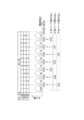
図7は、メモリセルトランジスタMTの閾値分布等を模式的に示す図である。図7の中段にある図は、メモリセルトランジスタMTの閾値電圧(横軸)と、メモリセルトランジスタMTの個数(縦軸)との対応関係を表している。 Figure 7 is a diagram showing a schematic of the threshold distribution of memory cell transistors MT. The diagram in the middle of Figure 7 shows the correspondence between the threshold voltage of memory cell transistors MT (horizontal axis) and the number of memory cell transistors MT (vertical axis).
本実施形態のようにTLC方式を採用した場合においては、複数のメモリセルトランジスタMTは、図7の中段に示されるように、8つの閾値分布を形成する。この8個の閾値分布(書き込みレベル)のことを、閾値電圧の低い方から順に“ER”レベル、“A”レベル、“B”レベル、“C”レベル、“D”レベル、“E”レベル、“F”レベル、“G”レベルと称する。 When the TLC method is adopted as in this embodiment, the multiple memory cell transistors MT form eight threshold distributions, as shown in the middle of Figure 7. These eight threshold distributions (write levels) are referred to as the "ER" level, "A" level, "B" level, "C" level, "D" level, "E" level, "F" level, and "G" level, in order from the lowest threshold voltage.
図7の上段にある表は、閾値電圧の上記各レベルのそれぞれに対応して、割り当てられるデータの例を表している。同表に示されるように、“ER”レベル、“A”レベル、“B”レベル、“C”レベル、“D”レベル、“E”レベル、“F”レベル、及び“G”レベルには、例えば以下に示すような、それぞれ異なる3ビットデータが割り当てられている。
“ER”レベル:“111”(“下位ビット/中位ビット/上位ビット”)
“A”レベル:“011”
“B”レベル:“001”
“C”レベル:“000”
“D”レベル:“010”
“E”レベル:“110”
“F”レベル:“100”
“G”レベル:“101”
7 shows an example of data assigned to each of the above threshold voltage levels. As shown in the table, different 3-bit data are assigned to the "ER" level, "A" level, "B" level, "C" level, "D" level, "E" level, "F" level, and "G" level, for example, as shown below.
"ER" level: "111"("lower bit/middle bit/upper bit")
"A" level: "011"
"B" level: "001"
"C" level: "000"
"D" level: "010"
"E" level: "110"
"F" level: "100"
"G" level: "101"
このように、本実施形態におけるメモリセルトランジスタMTの閾値電圧は、予め設定された8つの候補レベルのうちの1つをとり得るものとなっており、それぞれの候補レベルに対応して、上記のようにデータが割り当てられている。 In this way, the threshold voltage of the memory cell transistor MT in this embodiment can take one of eight preset candidate levels, and data is assigned to each candidate level as described above.
互いに隣り合う一対の閾値分布の間には、それぞれ書き込み動作で使用されるベリファイ電圧が設定される。具体的には、“A”レベル、“B”レベル、“C”レベル、“D”レベル、“E”レベル、“F”レベル、及び“G”レベルにそれぞれ対応して、ベリファイ電圧VfyA、VfyB、VfyC、VfyD、VfyE、VfyF、及びVfyGが設定される。 Between each pair of adjacent threshold distributions, a verify voltage is set to be used in the write operation. Specifically, verify voltages VfyA, VfyB, VfyC, VfyD, VfyE, VfyF, and VfyG are set to correspond to the "A" level, "B" level, "C" level, "D" level, "E" level, "F" level, and "G" level, respectively.
ベリファイ電圧VfyAは、“ER”レベルにおける最大の閾値電圧と“A”レベルにおける最小の閾値電圧との間に設定される。ワード線WLにベリファイ電圧VfyAが印加されると、当該ワード線WLに繋がるメモリセルトランジスタMTのうち、閾値電圧が“ER”レベルに含まれるメモリセルトランジスタMTがオン状態になり、閾値電圧が“A”レベル以上の閾値分布に含まれるメモリセルトランジスタMTがオフ状態になる。 The verify voltage VfyA is set between the maximum threshold voltage at the "ER" level and the minimum threshold voltage at the "A" level. When the verify voltage VfyA is applied to the word line WL, among the memory cell transistors MT connected to the word line WL, the memory cell transistors MT whose threshold voltage is included in the "ER" level are turned on, and the memory cell transistors MT whose threshold voltage is included in the threshold distribution at or above the "A" level are turned off.
その他のベリファイ電圧VfyB、VfyC、VfyD、VfyE、VfyF、及びVfyGも、上記のベリファイ電圧VfyAと同様に設定される。ベリファイ電圧VfyBは、“A”レベルと“B”レベルとの間に設定され、ベリファイ電圧VfyCは、“B”レベルと“C”レベルとの間に設定され、ベリファイ電圧VfyDは、“C”レベルと“D”レベルとの間に設定され、ベリファイ電圧VfyEは、“D”レベルと“E”レベルとの間に設定され、ベリファイ電圧VfyFは、“E”レベルと“F”レベルとの間に設定され、ベリファイ電圧VfyGは、“F”レベルと“G”レベルとの間に設定される。 The other verify voltages VfyB, VfyC, VfyD, VfyE, VfyF, and VfyG are set in the same manner as the verify voltage VfyA. The verify voltage VfyB is set between the "A" level and the "B" level, the verify voltage VfyC is set between the "B" level and the "C" level, the verify voltage VfyD is set between the "C" level and the "D" level, the verify voltage VfyE is set between the "D" level and the "E" level, the verify voltage VfyF is set between the "E" level and the "F" level, and the verify voltage VfyG is set between the "F" level and the "G" level.
例えば、ベリファイ電圧VfyAは0.8Vに、ベリファイ電圧VfyBは1.6Vに、ベリファイ電圧VfyCは2.4Vに、ベリファイ電圧VfyDは3.1Vに、ベリファイ電圧VfyEは3.8Vに、ベリファイ電圧VfyFは4.6Vに、ベリファイ電圧VfyGは5.6Vに、それぞれ設定してもよい。しかし、これに限定されることなく、ベリファイ電圧VfyA、VfyB、VfyC、VfyD、VfyE、VfyF、及びVfyGは、例えば、0V~7.0Vの範囲で、適宜、段階的に設定してもよい。 For example, verify voltage VfyA may be set to 0.8 V, verify voltage VfyB may be set to 1.6 V, verify voltage VfyC may be set to 2.4 V, verify voltage VfyD may be set to 3.1 V, verify voltage VfyE may be set to 3.8 V, verify voltage VfyF may be set to 4.6 V, and verify voltage VfyG may be set to 5.6 V. However, without being limited to this, verify voltages VfyA, VfyB, VfyC, VfyD, VfyE, VfyF, and VfyG may be set in stages as appropriate within the range of, for example, 0 V to 7.0 V.
また、隣り合う閾値分布の間には、それぞれ読み出し動作で使用される読み出し電圧が設定される。「読み出し電圧」とは、読み出し動作時において、読み出し対象となるメモリセルトランジスタMTに繋がるワード線WL、すなわち選択ワード線に対し印加される電圧である。読み出し動作では、読み出し対象となるメモリセルトランジスタMTの閾値電圧が、印加された読み出し電圧よりも高いか否かの判定結果に基づいてデータが決定される。 In addition, between adjacent threshold distributions, a read voltage is set to be used in the read operation. The "read voltage" is the voltage applied to the word line WL connected to the memory cell transistor MT to be read during the read operation, i.e., the selected word line. In the read operation, data is determined based on the result of determining whether the threshold voltage of the memory cell transistor MT to be read is higher than the applied read voltage.
図7の下段の図において模式的に示されるように、具体的には、メモリセルトランジスタMTの閾値電圧が“ER”レベルに含まれるのか“A”レベル以上に含まれるのかを判定する読み出し電圧VrAは、“ER”レベルにおける最大の閾値電圧と“A”レベルにおける最小の閾値電圧との間に設定される。 As shown in the lower diagram of FIG. 7, specifically, the read voltage VrA, which determines whether the threshold voltage of the memory cell transistor MT is included in the "ER" level or is included in the "A" level or higher, is set between the maximum threshold voltage at the "ER" level and the minimum threshold voltage at the "A" level.
その他の読み出し電圧VrB、VrC、VrD、VrE、VrF、及びVrGも、上記の読み出し電圧VrAと同様に設定される。読み出し電圧VrBは、“A”レベルと“B”レベルとの間に設定され、読み出し電圧VrCは、“B”レベルと“C”レベルとの間に設定され、読み出し電圧VrDは、“C”レベルと“D”レベルとの間に設定され、読み出し電圧VrEは、“D”レベルと“E”レベルとの間に設定され、読み出し電圧VrFは、“E”レベルと“F”レベルとの間に設定され、読み出し電圧VrGは、“F”レベルと“G”レベルとの間に設定される。 The other read voltages VrB, VrC, VrD, VrE, VrF, and VrG are set in the same manner as the read voltage VrA. The read voltage VrB is set between the "A" level and the "B" level, the read voltage VrC is set between the "B" level and the "C" level, the read voltage VrD is set between the "C" level and the "D" level, the read voltage VrE is set between the "D" level and the "E" level, the read voltage VrF is set between the "E" level and the "F" level, and the read voltage VrG is set between the "F" level and the "G" level.
そして、最も高い閾値分布(例えば“G”レベル)の最大の閾値電圧よりも高い電圧に、読み出しパス電圧VPASS_READが設定される。読み出しパス電圧VPASS_READがゲートに印加されたメモリセルトランジスタMTは、記憶するデータに依らずにオン状態になる。 Then, the read pass voltage VPASS_READ is set to a voltage higher than the maximum threshold voltage of the highest threshold distribution (e.g., the "G" level). The memory cell transistor MT to which the read pass voltage VPASS_READ is applied to its gate is turned on regardless of the data to be stored.
尚、ベリファイ電圧VfyA、VfyB、VfyC、VfyD、VfyE、VfyF、及びVfyGは、例えば、読み出し電圧VrA、VrB、VrC、VrD、VrE、VrF、及びVrGよりもそれぞれ高い電圧に設定される。つまり、ベリファイ電圧VfyA、VfyB、VfyC、VfyD、VfyE、VfyF、及びVfyGは、それぞれ“A”レベル、“B”レベル、“C”レベル、“D”レベル、“E”レベル、“F”レベル、及び“G”レベルの閾値分布の下裾近傍に設定される。 The verify voltages VfyA, VfyB, VfyC, VfyD, VfyE, VfyF, and VfyG are set to voltages higher than the read voltages VrA, VrB, VrC, VrD, VrE, VrF, and VrG, respectively. In other words, the verify voltages VfyA, VfyB, VfyC, VfyD, VfyE, VfyF, and VfyG are set near the lower tails of the threshold distributions of the "A" level, "B" level, "C" level, "D" level, "E" level, "F" level, and "G" level, respectively.
以上に説明したようなデータの割り付けが適用された場合、読み出し動作において下位ビットの1ページデータ(下位ページデータ)は、読み出し電圧VrA及びVrEを用いた読み出し結果によって確定させることができる。中位ビットの1ページデータ(中位ページデータ)は、読み出し電圧VrB、VrD、及びVrFを用いた読み出し結果によって確定させることができる。上位ビットの1ページデータ(上位ページデータ)は、読み出し電圧VrC及びVrGを用いた読み出し結果によって確定させることができる。このように、下位ページデータ、中位ページデータ、及び上位ページデータがそれぞれ、2回、3回、及び2回の読み出し動作によって確定するため、以上のようなデータの割り付けは“2-3-2コード”と称される。 When the data allocation described above is applied, one page of data of the lower bits (lower page data) in a read operation can be determined by the read result using read voltages VrA and VrE. One page of data of the middle bits (middle page data) can be determined by the read result using read voltages VrB, VrD, and VrF. One page of data of the upper bits (upper page data) can be determined by the read result using read voltages VrC and VrG. In this way, the lower page data, middle page data, and upper page data are determined by two, three, and two read operations, respectively, so the above data allocation is called a "2-3-2 code."
尚、以上で説明したようなデータの割り付けはあくまで一例であり、実際のデータの割り付けはこれに限定されない。例えば、2ビット又は4ビット以上のデータが1つのメモリセルトランジスタMTに記憶されてもよい。また、データが割り付けられる閾値分布の数(つまり、上記の「候補レベル」の数)は7以下であってもよく、9以上であってもよい。例えば、“2-3-2コード”に代えて、“1-3-3コード”又は“1-2-4コード”を用いてもよい。また、例えば、下位ビット/中位ビット/上位ビットの割り当てを変更してもよい。より具体的には、例えば、“2-3-2コード”において、下位ページデータを読み出し電圧VrC及びVrBを用いた読み出し結果によって確定させ、中位ページデータを読み出し電圧VrB、VrD、及びVrFを用いた読み出し結果によって確定させ、上位ページデータを読み出し電圧VrA及びVrEを用いた読み出し結果によって確定させるようにデータを割り当ててもよい。すなわち、例えば、下位ビットと上位ビットの割り当てを入れ換えてもよい。この場合、閾値電圧の各レベルのそれぞれに対応して、以下のようにデータが割り当てられる。
“ER”レベル:“111”(“下位ビット/中位ビット/上位ビット”)
“A”レベル:“110”
“B”レベル:“100”
“C”レベル:“000”
“D”レベル:“010”
“E”レベル:“011”
“F”レベル:“001”
“G”レベル:“101”
The data allocation described above is merely an example, and the actual data allocation is not limited to this. For example, 2-bit or 4-bit data or more may be stored in one memory cell transistor MT. The number of threshold distributions to which data is allocated (i.e., the number of the above-mentioned "candidate levels") may be 7 or less, or 9 or more. For example, instead of the "2-3-2 code", a "1-3-3 code" or a "1-2-4 code" may be used. Also, for example, the allocation of lower bits/middle bits/upper bits may be changed. More specifically, for example, in the "2-3-2 code", data may be allocated so that the lower page data is determined by the read result using the read voltages VrC and VrB, the middle page data is determined by the read result using the read voltages VrB, VrD, and VrF, and the upper page data is determined by the read result using the read voltages VrA and VrE. That is, for example, the allocation of the lower bits and the upper bits may be interchanged. In this case, data is allocated as follows in accordance with each level of the threshold voltage.
"ER" level: "111"("lower bit/middle bit/upper bit")
"A" level: "110"
"B" level: "100"
"C" level: "000"
"D" level: "010"
"E" level: "011"
"F" level: "001"
"G" level: "101"
半導体記憶装置2において行われる書き込み動作について説明する。書き込み動作では、プログラム動作及びベリファイ動作が行われる。「プログラム動作」とは、一部のメモリセルトランジスタMTの電荷蓄積層336に電子を注入することにより、当該メモリセルトランジスタMTの閾値電圧を変化させる動作のことである。「ベリファイ動作」とは、上記のプログラム動作の後、データを読み出すことで、メモリセルトランジスタMTの閾値電圧がターゲットレベルまで達したか否かを判定し検証する動作である。閾値電圧がターゲットレベルまで達したメモリセルトランジスタMTは、その後、書き込み禁止とされる。ここでいう「ターゲットレベル」とは、先に述べた8つの候補レベルの中から、目標のレベルとして設定された特定の候補レベルのことである。
The write operation performed in the
書き込み動作では、以上のプログラム動作及びベリファイ動作が繰り返し実行される。これにより、メモリセルトランジスタMTの閾値電圧がターゲットレベルまで上昇する。 During the write operation, the above program operation and verify operation are repeated. This causes the threshold voltage of the memory cell transistor MT to rise to the target level.
複数のワード線WLのうち、書き込み動作の対象(つまり、閾値電圧を変化させる対象)であるメモリセルトランジスタMTに繋がっているワード線WLのことを、以下では「選択ワード線」とも称する。また、書き込み動作の対象ではないメモリセルトランジスタMTに繋がっているワード線WLのことを、以下では「非選択ワード線」とも称する。書き込み対象であるメモリセルトランジスタMTのことを、以下では「選択メモリトランジスタ」とも称する。 Of the multiple word lines WL, the word line WL connected to the memory cell transistor MT that is the target of the write operation (i.e., the target for changing the threshold voltage) is also referred to as the "selected word line" below. Also, the word line WL connected to the memory cell transistor MT that is not the target of the write operation is also referred to as the "unselected word line" below. The memory cell transistor MT that is the target of the write operation is also referred to as the "selected memory transistor" below.
複数のストリングユニットSUのうち、書き込み動作の対象となるストリングユニットSUのことを、以下では「選択ストリングユニット」とも称する。また、書き込み動作の対象とはならないストリングユニットSUのことを、以下では「非選択ストリングユニット」とも称する。 Of the multiple string units SU, the string unit SU that is the target of the write operation is also referred to as the "selected string unit" below. Also, the string unit SU that is not the target of the write operation is also referred to as the "non-selected string unit" below.
選択ストリングユニットに含まれる各NANDストリングNSの導電体柱338、すなわち、選択ストリングユニットにおける各チャンネルのことを、以下では「選択チャンネル」とも称する。また、非選択ストリングユニットに含まれる各NANDストリングNSの導電体柱338、すなわち、非選択ストリングユニットにおける各チャンネルのことを、以下では「非選択チャンネル」とも称する。
The
複数のビット線BLのうち、選択メモリトランジスタに繋がっているビット線BLのことを、以下では「選択ビット線」とも称する。また、選択メモリトランジスタに繋がっていないビット線BLのことを、以下では「非選択ビット線」とも称する。 Of the multiple bit lines BL, the bit line BL connected to the selected memory transistor is also referred to as the "selected bit line" below. Also, the bit line BL that is not connected to the selected memory transistor is also referred to as the "unselected bit line" below.
プログラム動作について説明する。以下では、プログラム動作の対象がプレーンPL1である場合の例について説明するが、プレーンPL2の場合も以下と同様である。図8は、プログラム動作時における各配線の電位変化を示している。プログラム動作では、センスアンプ120が、プログラムデータに対応して各ビット線BLの電位を変化させる。プログラム対象の(閾値電圧を上昇させるべき)メモリセルトランジスタMTに繋がるビット線BLには、“L”レベルとして例えば接地電圧Vss(0V)が印加される。プログラム対象ではない(閾値電圧を維持させるべき)メモリセルトランジスタMTに繋がるビット線BLには、“H”レベルとして、例えば2.5Vが印加される。前者のビット線BLは、図8においては「BL(0)」と表記されている。後者のビット線BLは、図8においては「BL(1)」と表記されている。
The program operation will be described. In the following, an example in which the target of the program operation is the plane PL1 will be described, but the same applies to the case of the plane PL2. FIG. 8 shows the potential change of each wiring during the program operation. In the program operation, the
ロウデコーダ130は、書き込み動作の対象としていずれかのブロックBLKを選択し、更にいずれかのストリングユニットSUを選択する。より具体的には、選択されたストリングユニットSUにおけるセレクトゲート線SGD(選択セレクトゲート線SGDsel)には、電圧生成回路43からロウデコーダ130を介して例えば5Vが印加される。これにより、選択トランジスタST1はオン状態となる。他方で、セレクトゲート線SGSには、電圧生成回路43からロウデコーダ130を介して例えば電圧Vssが印加される。これにより、選択トランジスタST2はオフ状態となる。
The
また、選択ブロックBLKにおける非選択ストリングユニットSUのセレクトゲート線SGD(非選択セレクトゲート線SGDusel)には、電圧生成回路43からロウデコーダ130を介して例えば電圧5Vが印加される。これにより、選択トランジスタST1がオン状態となる。なお、各ブロックBLKに含まれるストリングユニットSUにおいて、セレクトゲート線SGSは共通に接続されている。従って、非選択ストリングユニットSUにおいても、選択トランジスタST2はオフ状態となる。
In addition, a voltage of, for example, 5V is applied to the select gate line SGD (unselected select gate line SGDusel) of the unselected string unit SU in the selected block BLK from the
更に、非選択ブロックBLKにおけるセレクトゲート線SGD及びセレクトゲート線SGSには、電圧生成回路43からロウデコーダ130を介して例えば電圧Vssが印加される。これにより、選択トランジスタST1及び選択トランジスタST2はオフ状態となる。
Furthermore, the voltage Vss, for example, is applied to the select gate line SGD and the select gate line SGS in the unselected block BLK from the
ソース線SLは、セレクトゲート線SGSの電位よりも高い電位とされる。当該電位は、例えば1Vである。 The source line SL is at a higher potential than the select gate line SGS. This potential is, for example, 1 V.
その後、選択ブロックBLKにおける選択セレクトゲート線SGDselの電位を、例えば2.5Vとする。この電位は、上記の例で0Vが与えられたビット線BL(0)に対応する選択トランジスタST1はオンさせるが、2.5Vが与えられたビット線BL(1)に対応する選択トランジスタST1はカットオフさせる電圧である。これにより、選択ストリングユニットSUにおいては、ビット線BL(0)に対応する選択トランジスタST1はオンされ、2.5Vが与えられたビット線BL(1)に対応する選択トランジスタST1はカットオフされる。一方で、非選択セレクトゲート線SGDuselの電位を、例えば電圧Vssとする。これにより、非選択ストリングユニットSUにおいては、ビット線BL(0)及びビット線BL(1)の電位に関わらず、選択トランジスタST1はカットオフされる。 Then, the potential of the selected select gate line SGDsel in the selected block BLK is set to, for example, 2.5V. This potential is a voltage that turns on the select transistor ST1 corresponding to the bit line BL(0) to which 0V is applied in the above example, but cuts off the select transistor ST1 corresponding to the bit line BL(1) to which 2.5V is applied. As a result, in the selected string unit SU, the select transistor ST1 corresponding to the bit line BL(0) is turned on, and the select transistor ST1 corresponding to the bit line BL(1) to which 2.5V is applied is cut off. On the other hand, the potential of the unselected select gate line SGDusel is set to, for example, voltage Vss. As a result, in the unselected string unit SU, the select transistor ST1 is cut off regardless of the potentials of the bit lines BL(0) and BL(1).
そしてロウデコーダ130は、選択ブロックBLKにおいて、書き込み動作の対象としていずれかのワード線WLを選択する。書き込み動作の対象となるワード線WL(選択ワード線WLsel)に、電圧生成回路43からロウデコーダ130を介して例えば電圧VPGMが印加される。一方で、その他のワード線WL(非選択ワード線WLusel)に、電圧生成回路43からロウデコーダ130を介して例えば電圧VPASS_PGMが印加される。電圧VPGMは、トンネル現象により電子を電荷蓄積層336に注入するための高電圧である。電圧VPASS_PGMは、ワード線WLに繋がるメモリセルトランジスタMTをONとする一方で、閾定電圧は変化させない程度の電圧である。VPGMはVPASS_PGMよりも高い電圧である。
Then, the
プログラム対象のビット線BL(0)に対応するNANDストリングNSでは、選択トランジスタST1がオン状態となる。そのため、選択ワード線WLselに接続されたメモリセルトランジスタMTのチャネル電位は0Vとなる。制御ゲートとチャネルとの間の電位差が大きくなり、その結果、電子が電荷蓄積層336に注入されるので、メモリセルトランジスタMTの閾値電圧が上昇される。
In the NAND string NS corresponding to the bit line BL(0) to be programmed, the select transistor ST1 is turned on. Therefore, the channel potential of the memory cell transistor MT connected to the selected word line WLsel becomes 0V. The potential difference between the control gate and the channel becomes large, and as a result, electrons are injected into the
プログラム対象ではないビット線BL(1)に対応するNANDストリングNSでは、選択トランジスタST1がカットオフ状態となる。そのため、選択ワード線WLselに接続されたメモリセルトランジスタMTのチャネルは電気的にフローティングとなり、ワード線WL等との容量カップリングによりチャネル電位は電圧VPGM近くまで上昇される。制御ゲートとチャネルとの間の電位差が小さくなり、その結果、電子は電荷蓄積層336に注入されないので、メモリセルトランジスタMTの閾値電圧は維持される。正確にいうと、閾値分布レベルがより高い分布に遷移するほどには、閾値電圧は変動しない。
In the NAND string NS corresponding to the bit line BL(1) that is not to be programmed, the select transistor ST1 is cut off. As a result, the channel of the memory cell transistor MT connected to the selected word line WLsel is electrically floating, and the channel potential is raised to close to the voltage VPGM due to capacitive coupling with the word line WL, etc. The potential difference between the control gate and the channel becomes small, and as a result, electrons are not injected into the
読み出し動作について説明する。以下では、読み出し動作の対象がプレーンPL1である場合の例について説明するが、プレーンPL2の場合も以下と同様である。プログラム動作に続いて行われるベリファイ動作は、以下に説明する読み出し動作と同じである。図9は、読み出し動作時における各配線の電位変化を示している。読み出し動作では、読み出し動作の対象となるメモリセルトランジスタMT、を含むNANDストリングNSが選択される。あるいは、読み出し動作の対象となるページを含むストリングユニットSUが選択される。 The read operation will be described. Below, an example will be described in which the target of the read operation is plane PL1, but the same applies to the case of plane PL2. The verify operation performed following the program operation is the same as the read operation described below. Figure 9 shows the potential changes of each wiring during a read operation. In a read operation, a NAND string NS including a memory cell transistor MT that is the target of the read operation is selected. Alternatively, a string unit SU including a page that is the target of the read operation is selected.
まず、選択セレクトゲート線SGDsel、非選択セレクトゲート線SGDusel及びセレクトゲート線SGSには、電圧生成回路43からロウデコーダ130を介して例えば5Vが印加される。これにより、選択ブロックBLKに含まれる選択トランジスタST1及び選択トランジスタST2はオン状態となる。また、選択ワード線WLsel及び非選択ワード線には、電圧生成回路43からロウデコーダ130を介して例えば読み出しパス電圧VPASS_READが印加される。読み出しパス電圧VPASS_READは、メモリセルトランジスタMTの閾値電圧にかかわらず、メモリセルトランジスタMTをONとすることができ、かつ、閾定電圧は変化させない程度の電圧である。これにより、選択ストリングユニットSUであるか非選択ストリングユニットSUであるかにかかわらず、選択ブロックBLKに含まれる全てのNANDストリングNSにおいて、電流が導通する。
First, a voltage of, for example, 5V is applied to the selected select gate line SGDsel, the unselected select gate line SGDusel, and the select gate line SGS from the
次に、読み出し動作の対象となるメモリセルトランジスタMTに繋がるワード線WL(選択ワード線WLsel)に対し、電圧生成回路43からロウデコーダ130を介して例えばVrAのような読み出し電圧Vrが印加される。それ以外のワード線(非選択ワード線WLusel)に対しては、読み出しパス電圧VPASS_READが印加される。
Next, a read voltage Vr, such as VrA, is applied from the
また、選択セレクトゲート線SGDsel及びセレクトゲート線SGSに印加する電圧は維持しつつ、非選択セレクトゲート線SGDuselには、電圧生成回路43からロウデコーダ130を介して例えば電圧Vssが印加される。これにより、選択ストリングユニットSUに含まれる選択トランジスタST1はオン状態を維持するが、非選択ストリングユニットSUに含まれる選択トランジスタST1はオフ状態となる。なお、選択ストリングユニットSUであるか非選択ストリングユニットSUであるかにかかわらず、選択ブロックBLKに含まれる選択トランジスタST2はオン状態となる。
While maintaining the voltage applied to the selected select gate line SGDsel and the select gate line SGS, the
これにより、非選択ストリングユニットSUに含まれるNANDストリングNSは、少なくとも選択トランジスタST1がオフ状態となるため、電流パスを形成しない。一方で、選択ストリングユニットSUに含まれるNANDストリングNSは、選択ワード線WLselに印加される読み出し電圧VrとメモリセルトランジスタMTの閾値電圧との関係に応じて、電流パスが形成され、または、形成されない。 As a result, the NAND string NS included in the unselected string unit SU does not form a current path because at least the selection transistor ST1 is in the off state. On the other hand, the NAND string NS included in the selected string unit SU forms or does not form a current path depending on the relationship between the read voltage Vr applied to the selected word line WLsel and the threshold voltage of the memory cell transistor MT.
センスアンプ120は、選択されたNANDストリングNSに繋がるビット線BLに対して電圧を印加する。この状態で、センスアンプ120は、当該ビット線BLを流れる電流の値に基づいてデータの読み出しを行う。具体的には、読み出し動作の対象となるメモリセルトランジスタMTの閾値電圧が、当該メモリセルトランジスタMTに印加された読み出し電圧よりも高いか否かを判定する。尚、データの読み出しは、ビット線BLを流れる電流の値に基づくのではなく、ビット線BLにおける電位の時間変化に基づいて行われてもよい。後者の場合、ビット線BLは、予め所定の電位となるようにプリチャージされる。
The
先に述べたベリファイ動作も、上記のような読み出し動作と同様に行われる。ベリファイ動作では、ベリファイの対象となるメモリセルトランジスタMTに繋がるワード線WLに対し、例えばVfyAのようなベリファイ電圧が電圧生成回路43からロウデコーダ130を介して印加されることとなる。
The verify operation described above is performed in the same manner as the read operation described above. In the verify operation, a verify voltage such as VfyA is applied from the
なお、先に述べたプログラム動作の初期段階における選択セレクトゲート線SGDsel及び非選択セレクトゲート線SGDuselに5Vの電圧を印加する動作は、省略される場合がある。同様に、先に述べた読み出し動作(ベリファイ動作)の初期段階における非選択セレクトゲート線SGDuselに5Vの電圧を印加し選択ワード線WLselに読み出しパス電圧VPASS_READを印加する動作は、省略される場合がある。 Note that the operation of applying a voltage of 5V to the selected select gate line SGDsel and the unselected select gate line SGDusel in the initial stage of the program operation described above may be omitted. Similarly, the operation of applying a voltage of 5V to the unselected select gate line SGDusel and applying a read pass voltage VPASS_READ to the selected word line WLsel in the initial stage of the read operation (verify operation) described above may be omitted.
読み出し動作時において、半導体記憶装置2とメモリコントローラ1との間で送受信される具体的な信号の流れ等について説明する。以下では、読み出し動作の対象がプレーンPL1である場合の例について説明するが、プレーンPL2の場合も以下と同様である。
The specific flow of signals transmitted and received between the
先ず、本実施形態の比較例について説明する。図10には、比較例に係る構成において、半導体記憶装置2とメモリコントローラ1との間で送受信される各種の信号等の例が示されている。
First, a comparative example of this embodiment will be described. FIG. 10 shows examples of various signals transmitted and received between the
読み出し動作時においては、メモリコントローラ1から半導体記憶装置2に向けて、信号DQ<7:0>として、「05h」、複数の「ADD」、及び「E0h」からなる信号が順に入力される。「05h」は、メモリセルアレイ110からのデータの読み出し動作を実行させるためのコマンドである。「ADD」は、データの読み出し元となるアドレスを指定する信号である。「E0h」は、読み出し動作を開始させるためのコマンドである。
During a read operation, signals consisting of "05h", multiple "ADD", and "E0h" are input in sequence as signal DQ<7:0> from the
図10では、「E0h」が半導体記憶装置2に入力されたタイミングが時刻t0として示されている。時刻t0から所定期間が経過した時刻t1において、メモリコントローラ1は、リードイネーブル信号/REのトグルを開始させる。先に述べたように、リードイネーブル信号/REは、メモリコントローラ1が、半導体記憶装置2からデータを読み出すための信号であり、半導体記憶装置2の入出力用パッド群31に入力される。時刻t1以降は、リードイネーブル信号/REが、HレベルとLレベルとの間において交互に切り換えられる(トグルされる)。このように切り換えられるリードイネーブル信号/REのそれぞれが、データを読み出すための「読み出し信号」として用いられる。入出力用パッド群31は、メモリコントローラ1から「読み出し信号」を繰り返し受信する「受信部」に該当する。
In FIG. 10, the timing when "E0h" is input to the
半導体記憶装置2は、リードイネーブル信号/REが切り換わる毎に(すなわち、それぞれの読み出し信号が入力される毎に)、信号DQ<7:0>としてデータを出力すると共に、データストローブ信号DQSをHレベルとLレベルとの間で切り換える。図10においては、信号DQ<7:0>として出力されるデータのそれぞれが「D」として示されている。また、最初のデータが出力され、データストローブ信号DQSが切り換わるタイミングが、時刻t2として示されている。メモリコントローラ1から入力されるリードイネーブル信号/REの切り換えと、半導体記憶装置2から出力されるデータストローブ信号DQSの切り換えと、の対応関係が、図10では点線の矢印で示されている。
The
尚、半導体記憶装置2からの読み出しデータの出力は、1つのデータを、偶数ビットからなるイーブンデータと、奇数ビットからなるオッドデータと、に分けた上で、それぞれを交互に出力することで行われる。図10において「D」と示されるそれぞれのデータは、イーブンデータ及びオッドデータのいずれかとして出力されるものである。
The output of read data from the
ところで、読み出し動作時において、プレーンPL1では、メモリセルトランジスタMTを含む多数のトランジスタを開閉動作させる必要がある。このとき、電圧生成回路43から各部へと出力される電流が増加するため、電源電圧が一時的に低下してしまうことがある。より具体的には、電源転圧をフィードバック制御によって制御している場合、電圧生成回路43から各部へと出力される電流が増加することにより、電源電圧が一時的に低下してしまうことがある。図10の最上段には、このように変動する電源電圧の変化の一例が示されている。この例において、電源電圧は、リードイネーブル信号/REのトグルが開始される時刻t0もしくはその近くから低下し始め、時刻t2以降においてもしばらくの間は目標電圧よりも低下してしまっている。このような電源電圧の低下が生じると、半導体記憶装置2におけるI/O出力特性が悪化し、読み出しデータの出力が不安定になってしまうことが懸念される。
During a read operation, the plane PL1 needs to open and close a large number of transistors, including the memory cell transistor MT. At this time, the current output from the
電源電圧の低下に対する対策としては、例えば、半導体記憶装置2を図11のように動作させることが考えられる。図11には、図10の比較例とは別の比較例において送受信される各種の信号等の例が示されている。
As a countermeasure against a drop in the power supply voltage, for example, it is possible to operate the
図11の比較例において、半導体記憶装置2は、図10の比較例と同様のタイミング(時刻t2)においてデータストローブ信号DQSのトグルを開始する。ただし、データストローブ信号DQSのトグルを開始してからしばらくの間は、半導体記憶装置2はメモリコントローラ1に向けてデータを出力しない。半導体記憶装置2からのデータの出力が開始されるのは、時刻t2よりも後の時刻t3からとなっている。この例における時刻t2から時刻t3までの期間の長さは、イーブンデータ又はオッドデータが計4つ出力され得る期間の長さ(換言すれば、2つのイーブンデータと2つのオッドデータが出力され得る期間の長さ)となっている。データストローブ信号DQSのトグルが開始されてから、メモリコントローラ1が要求するデータの出力が開始されるまでの期間のことを、以下では「レイテンシ期間」とも称する。
11, the
図11の比較例のようにレイテンシ期間を設けると、データの出力タイミングが時刻t2よりも遅くなるので、データ出力開始時点における電源電圧の一時的な低下を抑制できる。違う言い方をすると、図11の比較例のようにレイテンシ期間を設けると、データストローブ信号DQSのトグルが開始することによる電流の増加に起因する電源電圧の一時的な低下が抑制された状態で、データの出力を開始することができる。しかしながら、時刻t3においてデータの出力が開始されると、これによる電流の増加が生じることとなる。違う言い方をすると、図11の比較例のようにデータの出力開始をデータストローブ信号DQSのトグル開始から遅れさせたとしても、データの出願が開始することによる電流の増加に起因する電源電圧の一時的な低下による影響は避けることができない。 When a latency period is provided as in the comparative example of FIG. 11, the data output timing is delayed from time t2, so that a temporary drop in the power supply voltage at the start of data output can be suppressed. In other words, when a latency period is provided as in the comparative example of FIG. 11, data output can be started in a state in which a temporary drop in the power supply voltage caused by an increase in current due to the start of toggling of the data strobe signal DQS is suppressed. However, when data output starts at time t3, an increase in current occurs due to this. In other words, even if the start of data output is delayed from the start of toggling of the data strobe signal DQS as in the comparative example of FIG. 11, the effect of a temporary drop in the power supply voltage caused by an increase in current due to the start of data application cannot be avoided.
そこで、本実施形態に係る半導体記憶装置2では、読み出し動作時において以下のように動作する。図12には、本実施形態に係る半導体記憶装置2で送受信される各種の信号等の例が、図10や図11と同様の方法により示されている。
The
本実施形態においても、図11の例と同様のレイテンシ期間が設けられており、メモリコントローラ1が要求するデータの出力は時刻t3から開始される。ただし、本実施形態では、レイテンシ期間においても、半導体記憶装置2からメモリコントローラ1に向けてデータが出力される。この時出力されるデータは、メモリコントローラ1が要求するデータとは異なるダミーデータである。このようなダミーデータのことを、以下では「非正規データ」とも称する。また、メモリコントローラ1が要求する読み出しデータのことを、非正規データとは区別して以下では「正規データ」とも称する。図12では、信号DQ<7:0>として出力されるデータのうち、正規データを図10等と同様に「D」と表記しており、非正規データを「d」と表記している。尚、「d」として示されるそれぞれのデータは、イーブンデータ又はオッドデータのいずれかとして出力される個々のデータのことである。
In this embodiment, a latency period similar to that in the example of FIG. 11 is provided, and the output of data requested by the
本実施形態に係る半導体記憶装置2において、レイテンシ期間の開始時である時刻t2においては電圧生成回路43からの出力電流が増加するが、レイテンシ期間の終了時である時刻t3においては電圧生成回路43からの出力電流が増加しない。このため、図12に示すように、時刻t2の直後においては電源電圧が大きく低下するものの、時刻t3よりも前の時点では電源電圧がある程度回復している。本実施形態に係る半導体記憶装置2においては、図12に示すように、電源電圧が安定した後に、半導体記憶装置2からメモリコントローラ1に向けて正規データが送信されるので、I/O出力特性が悪化するという上記の問題を解消することができる。尚、メモリコントローラ1において、レイテンシ期間において入力される非正規データを無視する(例えば、受信後に破棄する)ように予め取り決めておけば、非正規データが読み出し動作に悪影響を及ぼしてしまうことは無い。
In the
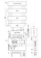
レイテンシ期間における非正規データ(d)の送信を可能とするための、半導体記憶装置2の具体的な構成について、図13を主に参照しながら説明する。同図においては、メモリセルアレイ110から入出力用パッド群31に至るまでの経路、すなわち、読み出しデータの流れる経路に沿った構成が模式的に描かれている。
The specific configuration of the
センスアンプ120には、先に述べた複数のセンスアンプユニットSAUと、複数のラッチ回路XDLと、マルチプレクサ121と、が含まれる。メモリセルアレイ110から読み出されたデータは、センスアンプユニットSAUからラッチ回路XDLへと送信され一旦保持された後、マルチプレクサ121を介して第1保持部510へと転送される。マルチプレクサ121と第1保持部510との間は、例えば128本の配線からなる第1データバス501により接続されている。なお、第1データバス501に含まれる配線の数は128本に限られない。第1データバス501に含まれる配線の数は、複数のラッチ回路XDLとマルチプレクサ121との間を繋いでいる配線の数よりも少ない。マルチプレクサ121は、複数のラッチ回路XDLから送信されるそれぞれのデータを、第1データバス501を介して、後段の第1保持部510へと順次転送する。
The
第1保持部510は、メモリセルアレイ110から読み出されたデータを複数保持するものであり、所謂「先入れ先出し」(FIFO:First In First Out)の動作を行うように構成された記憶装置である。第1保持部510は、マルチプレクサ121から転送されてきたデータを一時的複数保持し、当該データを、先に入力されていたものから順に入出力回路21に向けて出力する。第1保持部510と入出力回路21との間は、例えば16本の信号線からなる第2データバス502を介して接続されている。なお、第2データバス502に含まれる配線の数は16本に限られない。第1保持部510から入出力回路21へと入力されたデータは、次に述べる第2保持部520によって一時的に保持された後、入出力用パッド群31から信号DQ<7:0>として外部に出力される。
The
入出力回路21は、第2保持部520と、ライトポインタ生成回路541と、リードポインタ生成回路542と、マルチプレクサ531と、ドライバ532と、を有しており、これらを組み合わせてなる回路が、入出力用パッド群31が有する8つのパッド、すなわち、DQ<7:0>に対応する8つパッドのそれぞれに対応して個別に設けられている。つまり、入出力回路21においては、第2保持部520やマルチプレクサ531等のそれぞれが8つずつ設けられている。図13においては、これらのうちDQ<0>のパッドに接続されるもののみが図示されており、その他については図示が省略されている。
The input/
第2保持部520は、第1保持部510から送信されるデータを受け入れて、当該データを複数保持するものである。本実施形態の第2保持部520には、イーブンデータを保持する部分と、オッドデータを保持する部分とに分けられている。前者のことを、以下では「第2保持部521」とも表記する。後者のことを、以下では「第2保持部522」とも表記する。
The
第2保持部520は、先に述べた第1保持部510と同様に、所謂「先入れ先出し」(FIFO:First In First Out)の動作を行うように構成された記憶装置である。第2保持部520は、第1保持部510から入力されるデータを上記のように一時的に受け入れた後、当該データを、入力されたものから順にDQ<0>のパッドへと出力する。このようなデータの出力は、マルチプレクサ531及びドライバ532を介して、第2保持部521及び第2保持部522のそれぞれから交互に行われる。
The
ライトポインタ生成回路541は、ライトポインタWptrを生成する回路である。「ライトポインタWptr」とは、第1保持部510から送信されるデータを第2保持部520に保持させる際において、その保持位置(つまり書き込み位置)を指示するポインタのことである。
The write
リードポインタ生成回路542は、リードポインタRptrを生成する回路である。「リードポインタRptr」とは、第2保持部520からドライバ532に向けてデータを送信させる際において、第2保持部520における当該データの保持位置(つまり読み出し位置)を指示するポインタのことである。
The read
ライトポインタ生成回路541及びリードポインタ生成回路542からなる一対の回路は、第2保持部521及び第2保持部522のそれぞれについて設けられている。ただし、図13においては、第2保持部522について設けられたライトポインタ生成回路541及びリードポインタ生成回路542のみが図示されており、第2保持部521について設けられたライトポインタ生成回路541及びリードポインタ生成回路542の図示が省略されている。
A pair of circuits consisting of a write
第1保持部510から第2保持部520へのデータの送信、及び、第2保持部520からマルチプレクサ531へのデータの送信、のそれぞれは、シーケンサ41によって制御される。
The transmission of data from the
第2保持部520の構成、及びライトポインタ生成回路541やリードポインタ生成回路542の機能について説明する。図14には、第2保持部522の構成が模式的に描かれている。尚、第2保持部521の構成は、第2保持部522の構成と同じであるから、その説明を省略する。
The configuration of the
図14に示されるように、第2保持部522は、マルチプレクサM1と、複数のフリップフロップFFと、マルチプレクサM2と、を有している。尚、フリップフロップFFは第2保持部522において複数設けられているが、図14においては、これらのうちの3つのみが「FF1」、「FF2」、「FF3」として描かれている。
As shown in FIG. 14, the
マルチプレクサM1は、ライトポインタ生成回路541から入力されるライトポインタWptrに基づいて、いずれかのフリップフロップFFをデータの書き込み対象として選択し、当該フリップフロップFFにデータを送信する。
The multiplexer M1 selects one of the flip-flops FF to which data is to be written based on the write pointer Wptr input from the write
それぞれのフリップフロップFFは、第2保持部522における1ビットデータの記憶場所として機能する。フリップフロップFFは、入力されるクロック信号CLK1がLレベルからHレベルに立ち上がるタイミングで、それまで保持していたデータをマルチプレクサM2側へと出力すると共に、マルチプレクサM1側から入力される新たなデータを保持する。
Each flip-flop FF functions as a storage location for 1-bit data in the
クロック信号CLK1は、それぞれのフリップフロップFFがデータを取り込むタイミング、を規定する信号である。クロック信号CLK1はシーケンサ41により生成される。クロック信号CLK1は、後述のレイテンシ回路410及びライトポインタ生成回路541を介して、シーケンサ41からそれぞれのフリップフロップFFへと入力される。
The clock signal CLK1 is a signal that specifies the timing at which each flip-flop FF takes in data. The clock signal CLK1 is generated by the
ライトポインタ生成回路541は、入力されるクロック信号CLK1に基づいて、ライトポインタWptrを生成する。ライトポインタWptrは、クロック信号CLK1がLレベルからHレベルに立ち上がるタイミングで、ライトポインタ生成回路541によりインクリメントされる。ライトポインタWptrは、第1保持部510から入力されるデータを、どのフリップフロップFFに取り込むべきかを指定する信号である。ライトポインタWptrがインクリメントされて行くことで、データの書き込み対象となるフリップフロップFFが順次切り換えられて行くこととなる。
The write
マルチプレクサM2は、リードポインタ生成回路542から入力されるリードポインタRptrに基づいて、いずれかのフリップフロップFFをデータの読み出し対象として選択し、当該フリップフロップFFからデータを受信する。マルチプレクサM2は、リードポインタRptrがインクリメントされるタイミングで、当該データをマルチプレクサ531側へと出力する。
The multiplexer M2 selects one of the flip-flops FF as the data read target based on the read pointer Rptr input from the read
リードポインタRptrは、どのフリップフロップFFからのデータをマルチプレクサ531側へと出力するか、を指定すると共に、データの出力タイミングを指定する信号である。リードポインタRptrは、リードポインタ生成回路542によって生成され、リードポインタ生成回路542からマルチプレクサM2へと入力される。
The read pointer Rptr is a signal that specifies which flip-flop FF data is to be output to the
リードポインタ生成回路542は、入力されるクロック信号CLK2に基づいて、リードポインタRptrを生成する。リードポインタRptrは、クロック信号CLK2がLレベルからHレベルに立ち上がるタイミングで、リードポインタ生成回路542によりインクリメントされ、マルチプレクサM2へと入力される。リードポインタRptrがインクリメントされて行くことで、データの読み出し対象となるフリップフロップFFが順次切り換えられて行くこととなる。データの読み出し対象となるフリップフロップFFが切り換えられて行く順序は、データの書き込み対象となるフリップフロップFFが切り換えられて行く順序と同じである。これにより、第2保持部522による「先入れ先出し」の動作が実現される。
The read
クロック信号CLK2は、上記のようにリードポインタRptrの元となる信号である。クロック信号CLK2は、メモリコントローラ1から入力されるリードイネーブル信号/REに基づいて、シーケンサ41により生成される。図13に示されるように、クロック信号CLK2は、シーケンサ41からリードポインタ生成回路542に入力されると共に、マルチプレクサ531にも入力される。
The clock signal CLK2 is the signal that is the source of the read pointer Rptr as described above. The clock signal CLK2 is generated by the
マルチプレクサ531は、第2保持部521から入力されるイーブンデータと、第2保持部522から入力されるオッドデータと、を交互に受け入れて、これをドライバ532へと出力するものである。
The
尚、マルチプレクサM1からマルチプレクサM2に向かって、複数のフリップフロップFFが多段に並んでいるような構成であってもよい。また、先に述べた第1保持部510も、以上のような第2保持部522と同様の構成とすることができる。
In addition, a configuration in which multiple flip-flops FF are arranged in multiple stages from multiplexer M1 to multiplexer M2 may be used. Also, the
「先入れ先出し」の動作を行う第2保持部520は、複数のデータの記憶場所を所定順序に沿って並べたもの、であると理解することができる。図15には、このような第2保持部520の構成が模式的に描かれている。図15において横一列に並ぶよう描かれたそれぞれの矩形が、データの記憶場所(具体的にはフリップフロップFF)を表している。それぞれの記憶場所は、データの書き込み順序(及び読み込み順序)に沿って、図15では左から右へと一列に並ぶように描かれている。ライトポインタWptr及びリードポインタRptrのそれぞれは、矢印に沿って図15の右方向へとインクリメントされて行く。
The
図15(A)は、レイテンシ期間が設定されない場合において(レイテンシ期間の長さが0である場合において)、メモリコントローラ1からデータの読み出しコマンドが入力され、半導体記憶装置2においてデータの出力準備が完了した時点、における第2保持部520の状態を示している。図12の例においては、時刻t1の直前の状態である。半導体記憶装置2では、プリフェッチ動作(先読み動作)を行うことで、これから出力すべき一連のデータの一部を第2保持部520に保持した状態となっている。
Figure 15 (A) shows the state of the
図15(A)の例では、メモリコントローラ1の要求に応じて、正規データD0、D1、D2、D3・・・が出力される例が示されている。
The example in FIG. 15(A) shows an example in which normal data D0, D1, D2, D3, etc. are output in response to a request from
図15(B)は、レイテンシ期間が設定される場合において、メモリコントローラ1からデータの読み出しコマンドが入力され、半導体記憶装置2においてデータの出力準備が完了した時点、における第2保持部520の状態を示している。この場合、正規データD0、D1、D2、D3・・・が出力される前に、レイテンシ期間の長さに対応して、非正規データ・・・d3、d2、d1、d0が出力される。より具体的には、レイテンシ期間の長さが8である場合には、オッドデータに対応する第2保持部522からは、正規データD0、D1、D2、D3・・・(D0o、D1o、D2o、D3o・・・)が出力される前に、非正規データd3、d2、d1、d0(d3o、d2o、d1o、d0o)が出力される。同様に、イーブンデータに対応する第2保持部521からも、正規データD0、D1、D2、D3・・・(D0e、D1e、D2e、D3e・・・)が出力される前に、非正規データd3、d2、d1、d0(d3e、d2e、d1e、d0e)が出力される。
15B shows the state of the
レイテンシ期間が設定されない場合(レイテンシ期間の長さが0である場合)、図15(A)のように、リードポインタRptrは最初に出力されるD0の記憶場所を示す。しかしながら、本実施形態では、レイテンシ期間が設定された場合、その長さに応じてリードポインタRptrを予めマイナス側(図15では左側)の位置を示すように調整しておくことで、最初にD0とは異なるデータが出力されるようにする。当該処理は、例えば、シーケンサ41の制御によって行われる。
When no latency period is set (when the length of the latency period is 0), the read pointer Rptr points to the memory location of D0 that is to be output first, as shown in FIG. 15(A). However, in this embodiment, when a latency period is set, the read pointer Rptr is adjusted in advance to point to a position on the negative side (the left side in FIG. 15) according to the length of the latency period, so that data different from D0 is output first. This process is performed, for example, under the control of the
例えば、図15(B)の例のように、レイテンシ期間が設定されその長さが8である場合、オッドデータに対応する第2保持部522とイーブンデータに対応する第2保持部521とのそれぞれにおいて、最初の正規データ(D0)の保持位置から4回分だけマイナス側の位置となるようにリードポインタRptrを調整する。このようにリードポインタRptrをマイナス側の位置となるように調整することで、メモリコントローラ1には、正規データとしてD0e、D0o、D1e、D1o、D2o、D2e、D3o、D3e・・・が順に出力される前に、非正規データとしてd3e、d3o、d2e、d2o、d1e、d1o、d0e、d0oが順に出力される。
15B, when a latency period is set and its length is 8, the read pointer Rptr is adjusted so that it is four times more negative than the holding position of the first regular data (D0) in each of the
図15(B)のようにリードポインタRptrが調整された後に、データが出力される場合の信号の例が、図16に示されている。同図に示される「d3e」とは、第2保持部521からイーブンデータとして出力されるd3のデータを表しており、「d3o」とは、第2保持部522からオッドデータとして出力されるd3のデータを表している。「d2e」、「d2o」、「d1e」、「d1o」、「d0e」、「d0o」、や「D0e」、「D0o」、「D1e」、「D1o」、「D2e」、「D2o」、「D3e」、「D3o」、等のその他のデータについても同様である。
An example of a signal when data is output after the read pointer Rptr is adjusted as in FIG. 15(B) is shown in FIG. 16. In the figure, "d3e" represents the d3 data output as even data from the
レイテンシ期間における、第2保持部520のフリップフロップ回路FF1、FF2、FF3が保持するデータと、第2保持部520から出力されるデータとの関係を図18に示す。
Figure 18 shows the relationship between the data held by the flip-flop circuits FF1, FF2, and FF3 of the
レイテンシ期間が終了すると、第2保持部520は正規データの出力を開始する。レイテンシ期間終了後のデータ出力期間における、第2保持部520のフリップフロップ回路FF1、FF2、FF3が保持するデータと、第2保持部520から出力されるデータとの関係を図19及び図20に示す。
When the latency period ends, the
この例では、時刻t2から時刻t3までのレイテンシ期間の長さが、イーブンデータ又はオッドデータが計8つ出力され得る期間の長さ(換言すれば、4つのイーブンデータと4つのオッドデータが出力され得る期間の長さ)として設定されている。このため、第2保持部521、522のそれぞれで、上位のようにリードポインタRptrをマイナス側に4回分移動させておくことで、レイテンシ期間においては非正規データを出力し、レイテンシ期間の後においては正規データを出力するような動作を実現することができる。
In this example, the length of the latency period from time t2 to time t3 is set as the length of the period during which a total of eight even data or odd data can be output (in other words, the length of the period during which four even data and four odd data can be output). Therefore, by moving the read pointer Rptr four times to the negative side as in the upper level in each of the
ところで、第2保持部520から非正規データが出力されているレイテンシ期間において、仮に、ライトポインタWptrがインクリメントされてしまうと、今後出力されるべきデータの一部が、出力されないまま上書きされてしまう可能性がある。そこで、本実施形態に係る半導体記憶装置2では、第2保持部520から非正規データを送信させているレイテンシ期間において、シーケンサ41が、第1保持部510から第2保持部520へのデータの送信を一時的に停止させておくこととしている。
However, if the write pointer Wptr is incremented during the latency period when non-regular data is being output from the
図13に示されるレイテンシ回路410は、シーケンサ41から出力されるクロック信号CLK1を、後段の第1保持部510やライトポインタ生成回路541へと送信するものである。レイテンシ期間において、レイテンシ回路410は、クロック信号CLK1の送信を一時的に停止する。具体的には、シーケンサ41から入力されるクロック信号CLK1をカウントし、レイテンシ期間においてデータの更新を停止させておくべき所定回数だけカウントされた時点で、後段に向けたクロック信号CLK1の送出を開始する。
The
その結果、レイテンシ期間においては、第1保持部510から第2保持部520へのデータの送信が停止した状態となる。これにより、第2保持部520のデータが未送信のまま上書きされてしまうような事態が防止される。レイテンシ回路410は、シーケンサ41の一部として構成されてもよい。
As a result, during the latency period, data transmission from the
以上のように、本実施形態に係る半導体記憶装置2は、メモリセルアレイ110から読み出されたデータを一時的に複数保持する第1保持部510及び第2保持部520と、第2保持部520から繰り返し送信されるデータを外部のメモリコントローラ1に出力する出力部(ドライバ532や入出力用パッド群31)と、メモリコントローラ1から、データを読み出すための読み出し信号(リードイネーブル信号/RE)を繰り返し受信する受信部(ロジック制御用パッド群32やロジック制御回路22)と、それぞれの読み出し信号に対応して、第2保持部520から出力部へとデータを送信させる制御部(シーケンサ41)と、を備える。
As described above, the
制御部であるシーケンサ41は、受信部によって最初に所定回数だけ受信されたそれぞれの読み出し信号に対応するデータとして、メモリコントローラ1が要求するデータとは異なる非正規データを、保持部から出力部へと送信させ、受信部によってその後に受信された読み出し信号に対応するデータとして、メモリコントローラ1が要求するデータである正規データを、保持部から出力部へと送信させる。これにより、正規データの送信開始時までには、低下していた電源電圧を正常値近くまで復帰させておくことができるので、メモリコントローラ1に向けたデータの出力を安定して行うことが可能となる。
The
制御部であるシーケンサ41は、第2保持部520に保持されている複数のデータのうち、出力部に向けて次に送信されるデータ、の保持位置を示すリードポインタRptrを、上記の「所定回数」に応じて予め調整しておくことで、保持部から非正規データを送信させる。具体的には、シーケンサ41は、リードポインタRptrを、正規データの保持位置から上記所定回数に応じた数だけマイナス側となる保持位置を示すように、予め調整しておく。これにより、レイテンシ期間における非正規データの出力を容易に実現することができる。
The
尚、レイテンシ期間において非正規データを送信するような半導体記憶装置2の構成としては、図17に示される比較例の構成とすることも考えられる。この比較例では、入出力回路21にレイテンシ回路543が設けられている点において、本実施形態と異なっている。
As a configuration of the
レイテンシ回路543は、シーケンサ41から出力されるクロック信号CLK2を、後段のリードポインタ生成回路542へと送信するものである。レイテンシ期間において、レイテンシ回路543は、クロック信号CLK2の送信を一時的に停止する。具体的には、シーケンサ41から入力されるクロック信号CLK2をカウントし、レイテンシ期間においてデータの更新を停止させておくべき所定回数だけカウントされた時点で、後段に向けたクロック信号CLK2の送出を開始する。尚、マルチプレクサ531には、レイテンシ期間においてもクロック信号CLK2が送信され続ける。
The
この場合、レイテンシ期間においては、第2保持部520から出力されるデータが更新されず、(移動せず止まったままの)リードポインタRptrで示された同じデータが、非正規データとして送信され続けることとなる。レイテンシ期間が終了すると、本実施形態と同様に正規データの送信が開始される。
In this case, during the latency period, the data output from the
しかしながら、上記のようなレイテンシ回路543は、高速で切り換わるクロック信号CLK2をカウントする必要があるため、消費電力の比較的大きな高速のトランジスタ等で構成する必要がある。更に、レイテンシ期間が長くなり、カウントすべき回数が多くなると、より多くのトランジスタ等が必要となり、レイテンシ回路543は更に大規模なものとなってしまう。その結果、消費電力の増大や、回路の大型化に繋がる可能性がある。また、レイテンシ期間において第2保持部520から出力されるデータが更新されず、移動せず止まったままのリードポインタRptrで示された同じデータが、非正規データとして送信され続けることから、電圧生成回路に適切な電流負荷をかけることができない。
However, since the
これに対し、本実施形態では、レイテンシ期間において第2保持部520から出力されるデータの更新を一時的に停止する必要が無い。このため、比較例におけるレイテンシ回路543を設ける必要が無いため、消費電力の増大や、回路の大型化を回避できる。
In contrast, in this embodiment, there is no need to temporarily stop updating the data output from the
実施形態においては、第2保持部520が入出力回路21の中に設けられていた。しかし、第2保持部520の構成はこれに限られない。第2保持部520は、例えば、図21に示される変形例のように、第2データバス502を跨ぐように設けられてもよい。
In the embodiment, the
この変形例のように、例えば、第2保持部520のマルチプレクサM1と複数のフリップフロップFFを第1保持部510の直後に配置し、第2保持部520のマルチプレクサM2を入出力回路21の中に配置してもよい。この場合、ライトポインタ生成回路541はマルチプレクサM1と複数のフリップフロップFFの近傍に配置され、リードポインタ生成回路542はマルチプレクサM2の近傍に配置される。
As in this modified example, for example, the multiplexer M1 and the multiple flip-flops FF of the
第2保持部520を第2データバス502を跨ぐように配置する場合、第1保持部510と入出力回路21とを第2データバス502で接続する場合と比べて、配線数が増加する。例えば、第2データバス502が16本の配線で構成されているとすると、第2保持部520を第2データバス502を跨ぐように配置する場合、オッドデータに対応する第2保持部522とイーブンデータに対応する第2保持部521とがそれぞれ3つのフリップフロップFFを有している場合、第1保持部510と入出力回路21とを接続する配線は48本必要となる。しかし、配線数が増加したことに伴い、各配線を伝搬する信号の切り替え速度を遅くすることができる。これにより、信号を送受信するためのトランジスタの閾値電圧を低く設定する必要がなくなるため、データ転送に伴う半導体記憶装置2の消費電力を低減することができる。
When the
その一方で、ライトポインタ生成回路541を第1保持部510の近傍に配置することができる。ライトポインタ生成回路541と第1保持部510には、高速で遷移するクロック信号CLK1が供給される。従って、第2保持部520を第2データバス502を跨ぐように配置することにより、ライトポインタ生成回路541と第1保持部510とを近接して配置することができるため、クロック信号CLK1を伝搬させるための制御信号線を短くすることができる。これにより、データ転送に伴う半導体記憶装置2の消費電力をさらに低減することができる。
On the other hand, the write
また、実施形態においては、第1保持部510および第2保持部520のそれぞれが、複数のフリップフロップFFを含むものとして説明した。しかし、第1保持部510および第2保持部520の構成はこれに限られない。第1保持部510および第2保持部520のそれぞれは、複数のフリップフロップFFの代わりに、複数のラッチ回路によって構成されていてもよい。ライトポインタWptrに応じてデータを格納可能なデータ保持回路を用いることで、所謂「先入れ先出し」(FIFO:First In First Out)の動作を行うように構成されていればよい。
In the embodiment, the
以上、具体例を参照しつつ本実施形態について説明した。しかし、本開示はこれらの具体例に限定されるものではない。これら具体例に、当業者が適宜設計変更を加えたものも、本開示の特徴を備えている限り、本開示の範囲に包含される。前述した各具体例が備える各要素およびその配置、条件、形状などは、例示したものに限定されるわけではなく適宜変更することができる。前述した各具体例が備える各要素は、技術的な矛盾が生じない限り、適宜組み合わせを変えることができる。 The present embodiment has been described above with reference to specific examples. However, the present disclosure is not limited to these specific examples. Design modifications to these specific examples made by a person skilled in the art are also included within the scope of the present disclosure as long as they have the features of the present disclosure. The elements of each of the above-mentioned specific examples, as well as their arrangement, conditions, shape, etc., are not limited to those exemplified and can be modified as appropriate. The elements of each of the above-mentioned specific examples can be combined in different ways as appropriate, as long as no technical contradictions arise.
1:メモリコントローラ、2:半導体記憶装置、31:入出力用パッド群、32:ロジック制御用パッド群、41:シーケンサ、110,210:メモリセルアレイ、510:第1保持部、520:第2保持部。 1: memory controller, 2: semiconductor memory device, 31: input/output pad group, 32: logic control pad group, 41: sequencer, 110, 210: memory cell array, 510: first holding unit, 520: second holding unit.
Claims (5)
前記メモリセルアレイから読み出されたデータを一時的に複数保持する保持部と、
前記保持部から繰り返し送信されるデータを外部のメモリコントローラに出力する出力部と、
前記メモリコントローラから、データを読み出すための読み出し信号を繰り返し受信する受信部と、
それぞれの前記読み出し信号に対応して、前記保持部から前記出力部へとデータを送信させる制御部と、を備え、
前記制御部は、
前記受信部によって最初に所定回数だけ受信されたそれぞれの前記読み出し信号に対応するデータとして、前記メモリコントローラが要求するデータとは異なる非正規データを、前記保持部から前記出力部へと送信させ、
前記受信部によってその後に受信された前記読み出し信号に対応するデータとして、前記メモリコントローラが要求するデータである正規データを、前記保持部から前記出力部へと送信させるものであり、
前記制御部は、
前記保持部に保持されている複数のデータのうち、前記出力部に向けて次に送信されるデータ、の保持位置を示すリードポインタを、前記所定回数に応じて予め調整しておくことで、前記保持部から前記非正規データを送信させる、半導体記憶装置。 a memory cell array for storing data;
a holding unit that temporarily holds a plurality of pieces of data read from the memory cell array;
an output unit that outputs the data repeatedly transmitted from the holding unit to an external memory controller;
a receiving unit that repeatedly receives a read signal for reading data from the memory controller;
a control unit that transmits data from the holding unit to the output unit in response to each of the read signals;
The control unit is
transmit, from the holding unit to the output unit, non-normal data different from data requested by the memory controller as data corresponding to each of the read signals initially received a predetermined number of times by the receiving unit;
and transmitting normal data, which is data requested by the memory controller, from the holding unit to the output unit as data corresponding to the read signal subsequently received by the receiving unit;
The control unit is
A semiconductor memory device that transmits the irregular data from the holding unit by pre-adjusting a read pointer indicating a holding position of the data to be next transmitted to the output unit among the multiple data held in the holding unit according to the predetermined number of times.
前記リードポインタを、前記正規データの保持位置から、前記所定回数に応じた数だけマイナス側となる保持位置を示すように、予め調整しておく、請求項1に記載の半導体記憶装置。 The control unit is
2. The semiconductor memory device according to claim 1, wherein said read pointer is adjusted in advance so as to indicate a holding position which is on the negative side of a holding position of said normal data by a number corresponding to said predetermined number of times.
前記メモリセルアレイから読み出されたデータを複数保持する第1保持部と、
前記第1保持部から送信されるデータを複数保持する第2保持部と、を含み、
前記読み出し信号に対応した前記出力部へのデータの送信を、前記第2保持部から行うものであり、
前記制御部は、
前記第1保持部から前記第2保持部へのデータの送信、及び、前記第2保持部から前記出力部へのデータの送信、のそれぞれを制御する、請求項1又は2に記載の半導体記憶装置。 The holding portion is
a first holding unit that holds a plurality of data read from the memory cell array;
a second storage unit configured to store a plurality of data transmitted from the first storage unit;
The second holding unit transmits data corresponding to the read signal to the output unit,
The control unit is
3 . The semiconductor memory device according to claim 1 , further comprising: a control circuit configured to control data transmission from the first holding unit to the second holding unit and data transmission from the second holding unit to the output unit.
前記第2保持部から前記出力部へと前記非正規データを送信させている期間において、
前記第1保持部から前記第2保持部へのデータの送信を停止させる、請求項3に記載の半導体記憶装置。 The control unit is
During a period in which the irregular data is transmitted from the second holding unit to the output unit,
The semiconductor memory device according to claim 3 , further comprising: a step of stopping transmission of data from said first holding unit to said second holding unit.
Priority Applications (4)
| Application Number | Priority Date | Filing Date | Title |
|---|---|---|---|
| JP2022043340A JP7703473B2 (en) | 2022-03-18 | 2022-03-18 | Semiconductor memory device |
| TW111119512A TWI828162B (en) | 2022-03-18 | 2022-05-25 | semiconductor memory device |
| CN202210704968.7A CN116798491A (en) | 2022-03-18 | 2022-06-21 | Semiconductor memory device |
| US17/896,907 US12136469B2 (en) | 2022-03-18 | 2022-08-26 | Semiconductor memory device |
Applications Claiming Priority (1)
| Application Number | Priority Date | Filing Date | Title |
|---|---|---|---|
| JP2022043340A JP7703473B2 (en) | 2022-03-18 | 2022-03-18 | Semiconductor memory device |
Publications (2)
| Publication Number | Publication Date |
|---|---|
| JP2023137230A JP2023137230A (en) | 2023-09-29 |
| JP7703473B2 true JP7703473B2 (en) | 2025-07-07 |
Family
ID=88048606
Family Applications (1)
| Application Number | Title | Priority Date | Filing Date |
|---|---|---|---|
| JP2022043340A Active JP7703473B2 (en) | 2022-03-18 | 2022-03-18 | Semiconductor memory device |
Country Status (4)
| Country | Link |
|---|---|
| US (1) | US12136469B2 (en) |
| JP (1) | JP7703473B2 (en) |
| CN (1) | CN116798491A (en) |
| TW (1) | TWI828162B (en) |
Families Citing this family (2)
| Publication number | Priority date | Publication date | Assignee | Title |
|---|---|---|---|---|
| JP7608293B2 (en) * | 2021-08-17 | 2025-01-06 | キオクシア株式会社 | Memory device and memory system |
| US12027211B2 (en) * | 2022-05-26 | 2024-07-02 | Micron Technology, Inc. | Partial block handling protocol in a non-volatile memory device |
Citations (3)
| Publication number | Priority date | Publication date | Assignee | Title |
|---|---|---|---|---|
| JP2007220271A (en) | 2006-02-15 | 2007-08-30 | Samsung Electronics Co Ltd | Burst read circuit and burst data output method for semiconductor memory device |
| JP2014021892A (en) | 2012-07-23 | 2014-02-03 | Renesas Electronics Corp | Semiconductor device |
| WO2021049033A1 (en) | 2019-09-13 | 2021-03-18 | キオクシア株式会社 | Memory system |
Family Cites Families (6)
| Publication number | Priority date | Publication date | Assignee | Title |
|---|---|---|---|---|
| US6928494B1 (en) * | 2000-03-29 | 2005-08-09 | Intel Corporation | Method and apparatus for timing-dependant transfers using FIFOs |
| TW563132B (en) | 2001-10-09 | 2003-11-21 | Via Tech Inc | Common DRAM controller supports double-data-rate and quad-data-rate memory |
| TWI433150B (en) | 2009-07-27 | 2014-04-01 | Sunplus Technology Co Ltd | Apparatus and method for data strobe and timing variation detection of an sdram interface |
| JP2013034133A (en) * | 2011-08-02 | 2013-02-14 | Fujitsu Ltd | Transmission apparatus, transmitting-receiving system, and control method |
| US11562780B2 (en) * | 2019-10-04 | 2023-01-24 | Samsung Electronics Co., Ltd. | Memory device and memory system including the same |
| JP2021149659A (en) * | 2020-03-19 | 2021-09-27 | キオクシア株式会社 | Semiconductor integrated circuit, memory controller, and memory system |
-
2022
- 2022-03-18 JP JP2022043340A patent/JP7703473B2/en active Active
- 2022-05-25 TW TW111119512A patent/TWI828162B/en active
- 2022-06-21 CN CN202210704968.7A patent/CN116798491A/en active Pending
- 2022-08-26 US US17/896,907 patent/US12136469B2/en active Active
Patent Citations (3)
| Publication number | Priority date | Publication date | Assignee | Title |
|---|---|---|---|---|
| JP2007220271A (en) | 2006-02-15 | 2007-08-30 | Samsung Electronics Co Ltd | Burst read circuit and burst data output method for semiconductor memory device |
| JP2014021892A (en) | 2012-07-23 | 2014-02-03 | Renesas Electronics Corp | Semiconductor device |
| WO2021049033A1 (en) | 2019-09-13 | 2021-03-18 | キオクシア株式会社 | Memory system |
Also Published As
| Publication number | Publication date |
|---|---|
| TWI828162B (en) | 2024-01-01 |
| CN116798491A (en) | 2023-09-22 |
| TW202338801A (en) | 2023-10-01 |
| JP2023137230A (en) | 2023-09-29 |
| US12136469B2 (en) | 2024-11-05 |
| US20230298641A1 (en) | 2023-09-21 |
Similar Documents
| Publication | Publication Date | Title |
|---|---|---|
| JP5330136B2 (en) | Semiconductor memory device | |
| JP7614966B2 (en) | Semiconductor memory device | |
| US10026484B2 (en) | High-speed readable semiconductor storage device | |
| JP7703473B2 (en) | Semiconductor memory device | |
| JP2023130590A (en) | semiconductor storage device | |
| TWI838805B (en) | Semiconductor memory devices | |
| TWI767789B (en) | semiconductor memory device | |
| CN114203241B (en) | Semiconductor memory devices | |
| US20250299743A1 (en) | Semiconductor memory device and memory system | |
| TWI919676B (en) | Semiconductor memory devices | |
| US12125528B2 (en) | Semiconductor memory device | |
| CN115620777B (en) | Semiconductor memory devices | |
| US20240079067A1 (en) | Semiconductor memory device | |
| US20220284972A1 (en) | Semiconductor storage device | |
| TW202607736A (en) | Semiconductor memory devices | |
| JP2024178717A (en) | Semiconductor memory device | |
| JP2024136643A (en) | Semiconductor Device | |
| JP2026025363A (en) | semiconductor memory device |
Legal Events
| Date | Code | Title | Description |
|---|---|---|---|
| A621 | Written request for application examination |
Free format text: JAPANESE INTERMEDIATE CODE: A621 Effective date: 20240905 |
|
| TRDD | Decision of grant or rejection written | ||
| A01 | Written decision to grant a patent or to grant a registration (utility model) |
Free format text: JAPANESE INTERMEDIATE CODE: A01 Effective date: 20250527 |
|
| A977 | Report on retrieval |
Free format text: JAPANESE INTERMEDIATE CODE: A971007 Effective date: 20250530 |
|
| A61 | First payment of annual fees (during grant procedure) |
Free format text: JAPANESE INTERMEDIATE CODE: A61 Effective date: 20250625 |
|
| R150 | Certificate of patent or registration of utility model |
Ref document number: 7703473 Country of ref document: JP Free format text: JAPANESE INTERMEDIATE CODE: R150 |