JP7704007B2 - 半導体装置の製造方法 - Google Patents
半導体装置の製造方法 Download PDFInfo
- Publication number
- JP7704007B2 JP7704007B2 JP2021182833A JP2021182833A JP7704007B2 JP 7704007 B2 JP7704007 B2 JP 7704007B2 JP 2021182833 A JP2021182833 A JP 2021182833A JP 2021182833 A JP2021182833 A JP 2021182833A JP 7704007 B2 JP7704007 B2 JP 7704007B2
- Authority
- JP
- Japan
- Prior art keywords
- layer
- region
- concentration
- deep
- drift
- Prior art date
- Legal status (The legal status is an assumption and is not a legal conclusion. Google has not performed a legal analysis and makes no representation as to the accuracy of the status listed.)
- Active
Links
Images






Classifications
-
- H—ELECTRICITY
- H10—SEMICONDUCTOR DEVICES; ELECTRIC SOLID-STATE DEVICES NOT OTHERWISE PROVIDED FOR
- H10D—INORGANIC ELECTRIC SEMICONDUCTOR DEVICES
- H10D62/00—Semiconductor bodies, or regions thereof, of devices having potential barriers
- H10D62/10—Shapes, relative sizes or dispositions of the regions of the semiconductor bodies; Shapes of the semiconductor bodies
-
- H—ELECTRICITY
- H10—SEMICONDUCTOR DEVICES; ELECTRIC SOLID-STATE DEVICES NOT OTHERWISE PROVIDED FOR
- H10D—INORGANIC ELECTRIC SEMICONDUCTOR DEVICES
- H10D12/00—Bipolar devices controlled by the field effect, e.g. insulated-gate bipolar transistors [IGBT]
- H10D12/01—Manufacture or treatment
- H10D12/031—Manufacture or treatment of IGBTs
-
- H—ELECTRICITY
- H10—SEMICONDUCTOR DEVICES; ELECTRIC SOLID-STATE DEVICES NOT OTHERWISE PROVIDED FOR
- H10D—INORGANIC ELECTRIC SEMICONDUCTOR DEVICES
- H10D30/00—Field-effect transistors [FET]
- H10D30/60—Insulated-gate field-effect transistors [IGFET]
-
- H—ELECTRICITY
- H10—SEMICONDUCTOR DEVICES; ELECTRIC SOLID-STATE DEVICES NOT OTHERWISE PROVIDED FOR
- H10D—INORGANIC ELECTRIC SEMICONDUCTOR DEVICES
- H10D30/00—Field-effect transistors [FET]
- H10D30/60—Insulated-gate field-effect transistors [IGFET]
- H10D30/64—Double-diffused metal-oxide semiconductor [DMOS] FETs
- H10D30/66—Vertical DMOS [VDMOS] FETs
- H10D30/662—Vertical DMOS [VDMOS] FETs having a drift region having a doping concentration that is higher between adjacent body regions relative to other parts of the drift region
-
- H—ELECTRICITY
- H10—SEMICONDUCTOR DEVICES; ELECTRIC SOLID-STATE DEVICES NOT OTHERWISE PROVIDED FOR
- H10D—INORGANIC ELECTRIC SEMICONDUCTOR DEVICES
- H10D30/00—Field-effect transistors [FET]
- H10D30/60—Insulated-gate field-effect transistors [IGFET]
- H10D30/64—Double-diffused metal-oxide semiconductor [DMOS] FETs
- H10D30/66—Vertical DMOS [VDMOS] FETs
- H10D30/668—Vertical DMOS [VDMOS] FETs having trench gate electrodes, e.g. UMOS transistors
-
- H—ELECTRICITY
- H10—SEMICONDUCTOR DEVICES; ELECTRIC SOLID-STATE DEVICES NOT OTHERWISE PROVIDED FOR
- H10D—INORGANIC ELECTRIC SEMICONDUCTOR DEVICES
- H10D62/00—Semiconductor bodies, or regions thereof, of devices having potential barriers
- H10D62/10—Shapes, relative sizes or dispositions of the regions of the semiconductor bodies; Shapes of the semiconductor bodies
- H10D62/102—Constructional design considerations for preventing surface leakage or controlling electric field concentration
- H10D62/103—Constructional design considerations for preventing surface leakage or controlling electric field concentration for increasing or controlling the breakdown voltage of reverse-biased devices
- H10D62/105—Constructional design considerations for preventing surface leakage or controlling electric field concentration for increasing or controlling the breakdown voltage of reverse-biased devices by having particular doping profiles, shapes or arrangements of PN junctions; by having supplementary regions, e.g. junction termination extension [JTE]
-
- H—ELECTRICITY
- H10—SEMICONDUCTOR DEVICES; ELECTRIC SOLID-STATE DEVICES NOT OTHERWISE PROVIDED FOR
- H10D—INORGANIC ELECTRIC SEMICONDUCTOR DEVICES
- H10D62/00—Semiconductor bodies, or regions thereof, of devices having potential barriers
- H10D62/10—Shapes, relative sizes or dispositions of the regions of the semiconductor bodies; Shapes of the semiconductor bodies
- H10D62/102—Constructional design considerations for preventing surface leakage or controlling electric field concentration
- H10D62/103—Constructional design considerations for preventing surface leakage or controlling electric field concentration for increasing or controlling the breakdown voltage of reverse-biased devices
- H10D62/105—Constructional design considerations for preventing surface leakage or controlling electric field concentration for increasing or controlling the breakdown voltage of reverse-biased devices by having particular doping profiles, shapes or arrangements of PN junctions; by having supplementary regions, e.g. junction termination extension [JTE]
- H10D62/109—Reduced surface field [RESURF] PN junction structures
- H10D62/111—Multiple RESURF structures, e.g. double RESURF or 3D-RESURF structures
-
- H—ELECTRICITY
- H10—SEMICONDUCTOR DEVICES; ELECTRIC SOLID-STATE DEVICES NOT OTHERWISE PROVIDED FOR
- H10D—INORGANIC ELECTRIC SEMICONDUCTOR DEVICES
- H10D62/00—Semiconductor bodies, or regions thereof, of devices having potential barriers
- H10D62/10—Shapes, relative sizes or dispositions of the regions of the semiconductor bodies; Shapes of the semiconductor bodies
- H10D62/124—Shapes, relative sizes or dispositions of the regions of semiconductor bodies or of junctions between the regions
-
- H—ELECTRICITY
- H10—SEMICONDUCTOR DEVICES; ELECTRIC SOLID-STATE DEVICES NOT OTHERWISE PROVIDED FOR
- H10D—INORGANIC ELECTRIC SEMICONDUCTOR DEVICES
- H10D62/00—Semiconductor bodies, or regions thereof, of devices having potential barriers
- H10D62/10—Shapes, relative sizes or dispositions of the regions of the semiconductor bodies; Shapes of the semiconductor bodies
- H10D62/13—Semiconductor regions connected to electrodes carrying current to be rectified, amplified or switched, e.g. source or drain regions
- H10D62/149—Source or drain regions of field-effect devices
- H10D62/151—Source or drain regions of field-effect devices of IGFETs
- H10D62/156—Drain regions of DMOS transistors
- H10D62/157—Impurity concentrations or distributions
-
- H—ELECTRICITY
- H10—SEMICONDUCTOR DEVICES; ELECTRIC SOLID-STATE DEVICES NOT OTHERWISE PROVIDED FOR
- H10D—INORGANIC ELECTRIC SEMICONDUCTOR DEVICES
- H10D62/00—Semiconductor bodies, or regions thereof, of devices having potential barriers
- H10D62/10—Shapes, relative sizes or dispositions of the regions of the semiconductor bodies; Shapes of the semiconductor bodies
- H10D62/17—Semiconductor regions connected to electrodes not carrying current to be rectified, amplified or switched, e.g. channel regions
- H10D62/213—Channel regions of field-effect devices
- H10D62/221—Channel regions of field-effect devices of FETs
- H10D62/235—Channel regions of field-effect devices of FETs of IGFETs
- H10D62/292—Non-planar channels of IGFETs
-
- H—ELECTRICITY
- H10—SEMICONDUCTOR DEVICES; ELECTRIC SOLID-STATE DEVICES NOT OTHERWISE PROVIDED FOR
- H10D—INORGANIC ELECTRIC SEMICONDUCTOR DEVICES
- H10D62/00—Semiconductor bodies, or regions thereof, of devices having potential barriers
- H10D62/10—Shapes, relative sizes or dispositions of the regions of the semiconductor bodies; Shapes of the semiconductor bodies
- H10D62/17—Semiconductor regions connected to electrodes not carrying current to be rectified, amplified or switched, e.g. channel regions
- H10D62/213—Channel regions of field-effect devices
- H10D62/221—Channel regions of field-effect devices of FETs
- H10D62/235—Channel regions of field-effect devices of FETs of IGFETs
- H10D62/299—Channel regions of field-effect devices of FETs of IGFETs having lateral doping variations
-
- H—ELECTRICITY
- H10—SEMICONDUCTOR DEVICES; ELECTRIC SOLID-STATE DEVICES NOT OTHERWISE PROVIDED FOR
- H10D—INORGANIC ELECTRIC SEMICONDUCTOR DEVICES
- H10D62/00—Semiconductor bodies, or regions thereof, of devices having potential barriers
- H10D62/10—Shapes, relative sizes or dispositions of the regions of the semiconductor bodies; Shapes of the semiconductor bodies
- H10D62/17—Semiconductor regions connected to electrodes not carrying current to be rectified, amplified or switched, e.g. channel regions
- H10D62/393—Body regions of DMOS transistors or IGBTs
-
- H—ELECTRICITY
- H10—SEMICONDUCTOR DEVICES; ELECTRIC SOLID-STATE DEVICES NOT OTHERWISE PROVIDED FOR
- H10D—INORGANIC ELECTRIC SEMICONDUCTOR DEVICES
- H10D62/00—Semiconductor bodies, or regions thereof, of devices having potential barriers
- H10D62/80—Semiconductor bodies, or regions thereof, of devices having potential barriers characterised by the materials
- H10D62/83—Semiconductor bodies, or regions thereof, of devices having potential barriers characterised by the materials being Group IV materials, e.g. B-doped Si or undoped Ge
- H10D62/832—Semiconductor bodies, or regions thereof, of devices having potential barriers characterised by the materials being Group IV materials, e.g. B-doped Si or undoped Ge being Group IV materials comprising two or more elements, e.g. SiGe
- H10D62/8325—Silicon carbide
-
- H—ELECTRICITY
- H10—SEMICONDUCTOR DEVICES; ELECTRIC SOLID-STATE DEVICES NOT OTHERWISE PROVIDED FOR
- H10D—INORGANIC ELECTRIC SEMICONDUCTOR DEVICES
- H10D64/00—Electrodes of devices having potential barriers
- H10D64/20—Electrodes characterised by their shapes, relative sizes or dispositions
- H10D64/27—Electrodes not carrying the current to be rectified, amplified, oscillated or switched, e.g. gates
- H10D64/311—Gate electrodes for field-effect devices
- H10D64/411—Gate electrodes for field-effect devices for FETs
- H10D64/511—Gate electrodes for field-effect devices for FETs for IGFETs
- H10D64/512—Disposition of the gate electrodes, e.g. buried gates
- H10D64/513—Disposition of the gate electrodes, e.g. buried gates within recesses in the substrate, e.g. trench gates, groove gates or buried gates
-
- H—ELECTRICITY
- H10—SEMICONDUCTOR DEVICES; ELECTRIC SOLID-STATE DEVICES NOT OTHERWISE PROVIDED FOR
- H10P—GENERIC PROCESSES OR APPARATUS FOR THE MANUFACTURE OR TREATMENT OF DEVICES COVERED BY CLASS H10
- H10P30/00—Ion implantation into wafers, substrates or parts of devices
- H10P30/20—Ion implantation into wafers, substrates or parts of devices into semiconductor materials, e.g. for doping
- H10P30/202—Ion implantation into wafers, substrates or parts of devices into semiconductor materials, e.g. for doping characterised by the semiconductor materials
- H10P30/204—Ion implantation into wafers, substrates or parts of devices into semiconductor materials, e.g. for doping characterised by the semiconductor materials into Group IV semiconductors
- H10P30/2042—Ion implantation into wafers, substrates or parts of devices into semiconductor materials, e.g. for doping characterised by the semiconductor materials into Group IV semiconductors into crystalline silicon carbide
-
- H—ELECTRICITY
- H10—SEMICONDUCTOR DEVICES; ELECTRIC SOLID-STATE DEVICES NOT OTHERWISE PROVIDED FOR
- H10P—GENERIC PROCESSES OR APPARATUS FOR THE MANUFACTURE OR TREATMENT OF DEVICES COVERED BY CLASS H10
- H10P30/00—Ion implantation into wafers, substrates or parts of devices
- H10P30/20—Ion implantation into wafers, substrates or parts of devices into semiconductor materials, e.g. for doping
- H10P30/21—Ion implantation into wafers, substrates or parts of devices into semiconductor materials, e.g. for doping of electrically active species
-
- H—ELECTRICITY
- H10—SEMICONDUCTOR DEVICES; ELECTRIC SOLID-STATE DEVICES NOT OTHERWISE PROVIDED FOR
- H10D—INORGANIC ELECTRIC SEMICONDUCTOR DEVICES
- H10D12/00—Bipolar devices controlled by the field effect, e.g. insulated-gate bipolar transistors [IGBT]
- H10D12/411—Insulated-gate bipolar transistors [IGBT]
- H10D12/441—Vertical IGBTs
- H10D12/461—Vertical IGBTs having non-planar surfaces, e.g. having trenches, recesses or pillars in the surfaces of the emitter, base or collector regions
- H10D12/481—Vertical IGBTs having non-planar surfaces, e.g. having trenches, recesses or pillars in the surfaces of the emitter, base or collector regions having gate structures on slanted surfaces, on vertical surfaces, or in grooves, e.g. trench gate IGBTs
Landscapes
- Electrodes Of Semiconductors (AREA)
- Recrystallisation Techniques (AREA)
- Chemical & Material Sciences (AREA)
- Composite Materials (AREA)
Description
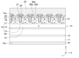
第1実施形態の半導体装置について、図面を参照しつつ説明する。本実施形態の半導体装置は、例えば、自動車等の車両に搭載され、車両用の各種電子装置を駆動するための装置として適用されると好適である。また、本実施形態では、トレンチゲート構造の反転型のMOSFETが形成されている炭化珪素(以下では、SiCともいう)半導体装置について説明する。なお、本実施形態では、MOSFETが形成されているセル領域の構成について説明するが、実際のSiC半導体装置には、セル領域を囲むように、FLR(Field Limiting Ringの略)構造等が形成された外周領域が備えられている。
上記第1実施形態の変形例について説明する。上記第1実施形態において、第1ディープ層15は、第1長さL1が第2長さL2より短くなる濃度プロファイルとされるのであれば、詳細な濃度プロファイルの形状は適宜変更可能である。例えば、図4Aに示されるように、第1ディープ層15は、第2位置P2が第1位置P1と一致し、第1長さL1が0となる濃度プロファイルとされていてもよい。また、図4Bに示されるように、第1ディープ層15は、第2位置P2と第1位置P1との間に段差Cを有する濃度プロファイルとされていてもよい。
本開示は、実施形態に準拠して記述されたが、本開示は当該実施形態や構造に限定されるものではないと理解される。本開示は、様々な変形例や均等範囲内の変形をも包含する。加えて、様々な組み合わせや形態、さらには、それらに一要素のみ、それ以上、あるいはそれ以下、を含む他の組み合わせや形態をも、本開示の範疇や思想範囲に入るものである。
15 ディープ層
15a 高濃度領域
15b 低濃度領域
19 ドリフト層
21 ベース層
22 ソース領域(不純物領域)
25 トレンチ
26 ゲート絶縁膜
27 ゲート電極
29 上部電極(第1電極)
30 下部電極(第2電極)
P1 第1位置
P2 第2位置
P3 第3位置
Claims (3)
- 第1導電型のドリフト層(19)と、
前記ドリフト層の表層部に形成された第2導電型のベース層(21)と、
前記ベース層の表層部に形成され、前記ドリフト層よりも高不純物濃度とされた第1導電型の不純物領域(22)と、
前記ベース層および前記不純物領域を貫通して前記ドリフト層に達するトレンチ(25)の壁面に形成されたゲート絶縁膜(26)と、前記ゲート絶縁膜上に形成されたゲート電極(27)とを有するトレンチゲート構造と、
前記ドリフト層のうちの前記トレンチの下方であって、前記トレンチと離れた状態で形成された第2導電型の第1ディープ層(15)と、
前記ベース層と前記第1ディープ層とを接続する第2導電型の第2ディープ層(18)と、
前記ドリフト層を挟んで前記ベース層と反対側に形成され、前記ドリフト層よりも高不純物濃度とされた第1導電型または第2導電型の高濃度層(11)と、
前記ベース層および前記不純物領域と電気的に接続される第1電極(29)と、
前記高濃度層と電気的に接続される第2電極(30)と、を備え、
前記ゲート電極に所定電圧以上のゲート電圧が印加されることで前記第1電極と前記第2電極との間に電流が流れるオン状態となると共に、前記ゲート電極に前記所定電圧未満のゲート電圧が印加されることでオフ状態となるように構成され、
前記第1ディープ層は、前記ドリフト層と前記ベース層との積層方向を深さ方向とした際の前記深さ方向に沿った不純物濃度の濃度プロファイルにおいて、不純物濃度が最大となる高濃度ピークを有し、前記オフ状態である際に空乏化しない領域を含む高濃度領域(15a)と、前記高濃度領域より前記高濃度層側に、前記深さ方向に沿った不純物濃度の変化の傾きが所定値未満となる領域を有し、前記オフ状態である際に空乏化する低濃度領域(15b)とを有する構成とされ、
前記第1ディープ層における最も前記ベース層側の位置を第1位置(P1)とし、前記高濃度ピークとなる位置を第2位置(P2)とし、前記低濃度領域における最も前記ベース層側の位置を第3位置(P3)とすると、前記第1位置と前記第3位置との間に前記高濃度領域が配置され、
前記第1位置と前記第2位置との間の第1長さ(L1)は、前記第2位置と前記第3位置との間の第2長さ(L2)よりも短くされている半導体装置の製造方法であって、
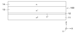
前記ドリフト層のうちの前記高濃度層側となる部分を含んで構成される構成基板(100)を用意することと、
前記構成基板にイオン注入を行って前記第1ディープ層を形成することと、
前記第1ディープ層上に構成層(17a)をエピタキシャル成長させることで前記第1ディープ層を内部に有する前記ドリフト層を形成することと、を行う半導体装置の製造方法。 - 前記ドリフト層を形成することでは、前記構成層にイオン注入を行うことにより、前記ドリフト層のうちの前記第1ディープ層との境界面を構成する部分の不純物濃度を調整する請求項1に記載の半導体装置の製造方法。
- 前記ドリフト層を形成することでは、前記構成層をエピタキシャル成長させる際に、前記構成層のうちの前記第1ディープ層との境界面を構成する部分の不純物濃度を調整する請求項1に記載の半導体装置の製造方法。
Priority Applications (3)
| Application Number | Priority Date | Filing Date | Title |
|---|---|---|---|
| JP2021182833A JP7704007B2 (ja) | 2021-11-09 | 2021-11-09 | 半導体装置の製造方法 |
| US17/977,420 US12426319B2 (en) | 2021-11-09 | 2022-10-31 | Semiconductor device and method for manufacturing the same |
| CN202211382957.8A CN116110934A (zh) | 2021-11-09 | 2022-11-07 | 半导体器件及其制造方法 |
Applications Claiming Priority (1)
| Application Number | Priority Date | Filing Date | Title |
|---|---|---|---|
| JP2021182833A JP7704007B2 (ja) | 2021-11-09 | 2021-11-09 | 半導体装置の製造方法 |
Publications (2)
| Publication Number | Publication Date |
|---|---|
| JP2023070568A JP2023070568A (ja) | 2023-05-19 |
| JP7704007B2 true JP7704007B2 (ja) | 2025-07-08 |
Family
ID=86229899
Family Applications (1)
| Application Number | Title | Priority Date | Filing Date |
|---|---|---|---|
| JP2021182833A Active JP7704007B2 (ja) | 2021-11-09 | 2021-11-09 | 半導体装置の製造方法 |
Country Status (3)
| Country | Link |
|---|---|
| US (1) | US12426319B2 (ja) |
| JP (1) | JP7704007B2 (ja) |
| CN (1) | CN116110934A (ja) |
Families Citing this family (3)
| Publication number | Priority date | Publication date | Assignee | Title |
|---|---|---|---|---|
| JP6981890B2 (ja) * | 2018-01-29 | 2021-12-17 | ルネサスエレクトロニクス株式会社 | 半導体装置 |
| JP7704007B2 (ja) * | 2021-11-09 | 2025-07-08 | 株式会社デンソー | 半導体装置の製造方法 |
| CN120264819B (zh) * | 2025-06-04 | 2025-09-26 | 杭州谱析光晶半导体科技有限公司 | 一种具有沟槽隔离和改进通道结构的垂直d-mosfet及制备方法 |
Citations (4)
| Publication number | Priority date | Publication date | Assignee | Title |
|---|---|---|---|---|
| JP2012169384A (ja) | 2011-02-11 | 2012-09-06 | Denso Corp | 炭化珪素半導体装置およびその製造方法 |
| JP2019046908A (ja) | 2017-08-31 | 2019-03-22 | 株式会社デンソー | 炭化珪素半導体装置およびその製造方法 |
| JP2020120072A (ja) | 2019-01-28 | 2020-08-06 | 株式会社デンソー | 半導体装置 |
| JP2021072359A (ja) | 2019-10-30 | 2021-05-06 | 株式会社デンソー | 炭化珪素半導体装置およびその製造方法 |
Family Cites Families (3)
| Publication number | Priority date | Publication date | Assignee | Title |
|---|---|---|---|---|
| JP2015072999A (ja) * | 2013-10-02 | 2015-04-16 | 株式会社デンソー | 炭化珪素半導体装置 |
| JP6811118B2 (ja) | 2017-02-27 | 2021-01-13 | 株式会社豊田中央研究所 | Mosfet |
| JP7704007B2 (ja) * | 2021-11-09 | 2025-07-08 | 株式会社デンソー | 半導体装置の製造方法 |
-
2021
- 2021-11-09 JP JP2021182833A patent/JP7704007B2/ja active Active
-
2022
- 2022-10-31 US US17/977,420 patent/US12426319B2/en active Active
- 2022-11-07 CN CN202211382957.8A patent/CN116110934A/zh active Pending
Patent Citations (4)
| Publication number | Priority date | Publication date | Assignee | Title |
|---|---|---|---|---|
| JP2012169384A (ja) | 2011-02-11 | 2012-09-06 | Denso Corp | 炭化珪素半導体装置およびその製造方法 |
| JP2019046908A (ja) | 2017-08-31 | 2019-03-22 | 株式会社デンソー | 炭化珪素半導体装置およびその製造方法 |
| JP2020120072A (ja) | 2019-01-28 | 2020-08-06 | 株式会社デンソー | 半導体装置 |
| JP2021072359A (ja) | 2019-10-30 | 2021-05-06 | 株式会社デンソー | 炭化珪素半導体装置およびその製造方法 |
Also Published As
| Publication number | Publication date |
|---|---|
| US12426319B2 (en) | 2025-09-23 |
| CN116110934A (zh) | 2023-05-12 |
| US20230143618A1 (en) | 2023-05-11 |
| JP2023070568A (ja) | 2023-05-19 |
Similar Documents
| Publication | Publication Date | Title |
|---|---|---|
| JP5728992B2 (ja) | 炭化珪素半導体装置およびその製造方法 | |
| US9818860B2 (en) | Silicon carbide semiconductor device and method for producing the same | |
| JP4577355B2 (ja) | 炭化珪素半導体装置およびその製造方法 | |
| JP2012169384A (ja) | 炭化珪素半導体装置およびその製造方法 | |
| JP7593225B2 (ja) | 炭化珪素半導体装置 | |
| JP2019046908A (ja) | 炭化珪素半導体装置およびその製造方法 | |
| JP2012169385A (ja) | 炭化珪素半導体装置 | |
| JP2015072999A (ja) | 炭化珪素半導体装置 | |
| JP2013214661A (ja) | 炭化珪素半導体装置およびその製造方法 | |
| JP7704007B2 (ja) | 半導体装置の製造方法 | |
| JP2009200300A (ja) | 半導体装置およびその製造方法 | |
| TWI760453B (zh) | 半導體裝置之製造方法 | |
| WO2023112547A1 (ja) | 半導体装置 | |
| JP7683466B2 (ja) | 半導体装置およびその製造方法 | |
| US9825125B2 (en) | Silicon carbide semiconductor device and manufacturing method of silicon carbide semiconductor device | |
| JP7439746B2 (ja) | 炭化珪素半導体装置 | |
| JP7439417B2 (ja) | 超接合半導体装置および超接合半導体装置の製造方法 | |
| JP7803229B2 (ja) | 炭化珪素半導体装置 | |
| JP2023056697A (ja) | 半導体装置およびその製造方法 | |
| CN117581382A (zh) | 半导体装置和半导体装置的制造方法 | |
| CN114388612A (zh) | 半导体装置及半导体装置的制造方法 | |
| JP2022182509A (ja) | 半導体装置およびその製造方法 | |
| JP7806602B2 (ja) | 半導体装置 | |
| US12622026B2 (en) | Semiconductor device and method for manufacturing the same | |
| WO2025258666A1 (ja) | 半導体装置 |
Legal Events
| Date | Code | Title | Description |
|---|---|---|---|
| A621 | Written request for application examination |
Free format text: JAPANESE INTERMEDIATE CODE: A621 Effective date: 20240510 |
|
| A977 | Report on retrieval |
Free format text: JAPANESE INTERMEDIATE CODE: A971007 Effective date: 20250123 |
|
| A131 | Notification of reasons for refusal |
Free format text: JAPANESE INTERMEDIATE CODE: A131 Effective date: 20250218 |
|
| A521 | Request for written amendment filed |
Free format text: JAPANESE INTERMEDIATE CODE: A523 Effective date: 20250415 |
|
| TRDD | Decision of grant or rejection written | ||
| A01 | Written decision to grant a patent or to grant a registration (utility model) |
Free format text: JAPANESE INTERMEDIATE CODE: A01 Effective date: 20250527 |
|
| A61 | First payment of annual fees (during grant procedure) |
Free format text: JAPANESE INTERMEDIATE CODE: A61 Effective date: 20250609 |
|
| R150 | Certificate of patent or registration of utility model |
Ref document number: 7704007 Country of ref document: JP Free format text: JAPANESE INTERMEDIATE CODE: R150 |