JPWO2005073743A1 - Rotation angle sensor, method for manufacturing the same, and throttle control device including the rotation angle sensor - Google Patents
Rotation angle sensor, method for manufacturing the same, and throttle control device including the rotation angle sensor Download PDFInfo
- Publication number
- JPWO2005073743A1 JPWO2005073743A1 JP2005517520A JP2005517520A JPWO2005073743A1 JP WO2005073743 A1 JPWO2005073743 A1 JP WO2005073743A1 JP 2005517520 A JP2005517520 A JP 2005517520A JP 2005517520 A JP2005517520 A JP 2005517520A JP WO2005073743 A1 JPWO2005073743 A1 JP WO2005073743A1
- Authority
- JP
- Japan
- Prior art keywords
- terminal
- sensor
- rotation angle
- angle sensor
- connection
- Prior art date
- Legal status (The legal status is an assumption and is not a legal conclusion. Google has not performed a legal analysis and makes no representation as to the accuracy of the status listed.)
- Granted
Links
- 238000004519 manufacturing process Methods 0.000 title claims abstract description 19
- 238000000034 method Methods 0.000 title description 2
- 238000004382 potting Methods 0.000 claims abstract description 55
- 239000000463 material Substances 0.000 claims abstract description 53
- 239000003990 capacitor Substances 0.000 claims description 178
- 238000001514 detection method Methods 0.000 claims description 106
- 229920005989 resin Polymers 0.000 claims description 93
- 239000011347 resin Substances 0.000 claims description 93
- 238000003466 welding Methods 0.000 claims description 63
- 238000000465 moulding Methods 0.000 claims description 61
- 230000003014 reinforcing effect Effects 0.000 claims description 6
- 239000002184 metal Substances 0.000 description 9
- 229910052751 metal Inorganic materials 0.000 description 9
- 238000005476 soldering Methods 0.000 description 9
- 238000005452 bending Methods 0.000 description 6
- 238000005520 cutting process Methods 0.000 description 6
- 230000007547 defect Effects 0.000 description 6
- 238000006073 displacement reaction Methods 0.000 description 5
- 229910000881 Cu alloy Inorganic materials 0.000 description 4
- 230000004308 accommodation Effects 0.000 description 4
- 239000003822 epoxy resin Substances 0.000 description 4
- 238000002347 injection Methods 0.000 description 4
- 239000007924 injection Substances 0.000 description 4
- 238000003780 insertion Methods 0.000 description 4
- 230000037431 insertion Effects 0.000 description 4
- 230000002093 peripheral effect Effects 0.000 description 4
- 229920000647 polyepoxide Polymers 0.000 description 4
- 230000008646 thermal stress Effects 0.000 description 4
- 239000004020 conductor Substances 0.000 description 3
- 239000010931 gold Substances 0.000 description 3
- 230000007246 mechanism Effects 0.000 description 3
- 230000009467 reduction Effects 0.000 description 3
- 229910000859 α-Fe Inorganic materials 0.000 description 3
- XUIMIQQOPSSXEZ-UHFFFAOYSA-N Silicon Chemical compound [Si] XUIMIQQOPSSXEZ-UHFFFAOYSA-N 0.000 description 2
- 230000006378 damage Effects 0.000 description 2
- 230000005611 electricity Effects 0.000 description 2
- 239000000696 magnetic material Substances 0.000 description 2
- 238000013508 migration Methods 0.000 description 2
- 230000005012 migration Effects 0.000 description 2
- 238000012986 modification Methods 0.000 description 2
- 230000004048 modification Effects 0.000 description 2
- 238000007747 plating Methods 0.000 description 2
- 229910052710 silicon Inorganic materials 0.000 description 2
- 239000010703 silicon Substances 0.000 description 2
- 229910000679 solder Inorganic materials 0.000 description 2
- 230000003068 static effect Effects 0.000 description 2
- 239000011800 void material Substances 0.000 description 2
- XLYOFNOQVPJJNP-UHFFFAOYSA-N water Substances O XLYOFNOQVPJJNP-UHFFFAOYSA-N 0.000 description 2
- 230000005540 biological transmission Effects 0.000 description 1
- 230000015572 biosynthetic process Effects 0.000 description 1
- 230000008859 change Effects 0.000 description 1
- 238000012937 correction Methods 0.000 description 1
- 238000011161 development Methods 0.000 description 1
- 230000000694 effects Effects 0.000 description 1
- 239000000446 fuel Substances 0.000 description 1
- PCHJSUWPFVWCPO-UHFFFAOYSA-N gold Chemical compound [Au] PCHJSUWPFVWCPO-UHFFFAOYSA-N 0.000 description 1
- 229910052737 gold Inorganic materials 0.000 description 1
- 238000001746 injection moulding Methods 0.000 description 1
- 238000009434 installation Methods 0.000 description 1
- 230000005415 magnetization Effects 0.000 description 1
- 230000000149 penetrating effect Effects 0.000 description 1
- 230000002265 prevention Effects 0.000 description 1
- 238000012545 processing Methods 0.000 description 1
- 229910052761 rare earth metal Inorganic materials 0.000 description 1
- 150000002910 rare earth metals Chemical class 0.000 description 1
- 230000000717 retained effect Effects 0.000 description 1
- 238000007493 shaping process Methods 0.000 description 1
- 238000009751 slip forming Methods 0.000 description 1
- 238000011144 upstream manufacturing Methods 0.000 description 1
Images


Classifications
-
- G—PHYSICS
- G01—MEASURING; TESTING
- G01D—MEASURING NOT SPECIALLY ADAPTED FOR A SPECIFIC VARIABLE; ARRANGEMENTS FOR MEASURING TWO OR MORE VARIABLES NOT COVERED IN A SINGLE OTHER SUBCLASS; TARIFF METERING APPARATUS; MEASURING OR TESTING NOT OTHERWISE PROVIDED FOR
- G01D5/00—Mechanical means for transferring the output of a sensing member; Means for converting the output of a sensing member to another variable where the form or nature of the sensing member does not constrain the means for converting; Transducers not specially adapted for a specific variable
- G01D5/12—Mechanical means for transferring the output of a sensing member; Means for converting the output of a sensing member to another variable where the form or nature of the sensing member does not constrain the means for converting; Transducers not specially adapted for a specific variable using electric or magnetic means
- G01D5/14—Mechanical means for transferring the output of a sensing member; Means for converting the output of a sensing member to another variable where the form or nature of the sensing member does not constrain the means for converting; Transducers not specially adapted for a specific variable using electric or magnetic means influencing the magnitude of a current or voltage
- G01D5/142—Mechanical means for transferring the output of a sensing member; Means for converting the output of a sensing member to another variable where the form or nature of the sensing member does not constrain the means for converting; Transducers not specially adapted for a specific variable using electric or magnetic means influencing the magnitude of a current or voltage using Hall-effect devices
- G01D5/145—Mechanical means for transferring the output of a sensing member; Means for converting the output of a sensing member to another variable where the form or nature of the sensing member does not constrain the means for converting; Transducers not specially adapted for a specific variable using electric or magnetic means influencing the magnitude of a current or voltage using Hall-effect devices influenced by the relative movement between the Hall device and magnetic fields
-
- F—MECHANICAL ENGINEERING; LIGHTING; HEATING; WEAPONS; BLASTING
- F02—COMBUSTION ENGINES; HOT-GAS OR COMBUSTION-PRODUCT ENGINE PLANTS
- F02D—CONTROLLING COMBUSTION ENGINES
- F02D9/00—Controlling engines by throttling air or fuel-and-air induction conduits or exhaust conduits
- F02D9/08—Throttle valves specially adapted therefor; Arrangements of such valves in conduits
- F02D9/10—Throttle valves specially adapted therefor; Arrangements of such valves in conduits having pivotally-mounted flaps
- F02D9/1035—Details of the valve housing
- F02D9/105—Details of the valve housing having a throttle position sensor
-
- F—MECHANICAL ENGINEERING; LIGHTING; HEATING; WEAPONS; BLASTING
- F02—COMBUSTION ENGINES; HOT-GAS OR COMBUSTION-PRODUCT ENGINE PLANTS
- F02D—CONTROLLING COMBUSTION ENGINES
- F02D11/00—Arrangements for, or adaptations to, non-automatic engine control initiation means, e.g. operator initiated
- F02D11/06—Arrangements for, or adaptations to, non-automatic engine control initiation means, e.g. operator initiated characterised by non-mechanical control linkages, e.g. fluid control linkages or by control linkages with power drive or assistance
- F02D11/10—Arrangements for, or adaptations to, non-automatic engine control initiation means, e.g. operator initiated characterised by non-mechanical control linkages, e.g. fluid control linkages or by control linkages with power drive or assistance of the electric type
- F02D11/106—Detection of demand or actuation
-
- Y—GENERAL TAGGING OF NEW TECHNOLOGICAL DEVELOPMENTS; GENERAL TAGGING OF CROSS-SECTIONAL TECHNOLOGIES SPANNING OVER SEVERAL SECTIONS OF THE IPC; TECHNICAL SUBJECTS COVERED BY FORMER USPC CROSS-REFERENCE ART COLLECTIONS [XRACs] AND DIGESTS
- Y10—TECHNICAL SUBJECTS COVERED BY FORMER USPC
- Y10T—TECHNICAL SUBJECTS COVERED BY FORMER US CLASSIFICATION
- Y10T29/00—Metal working
- Y10T29/49—Method of mechanical manufacture
- Y10T29/49002—Electrical device making
- Y10T29/49117—Conductor or circuit manufacturing
- Y10T29/49124—On flat or curved insulated base, e.g., printed circuit, etc.
- Y10T29/4913—Assembling to base an electrical component, e.g., capacitor, etc.
- Y10T29/49146—Assembling to base an electrical component, e.g., capacitor, etc. with encapsulating, e.g., potting, etc.
Landscapes
- Engineering & Computer Science (AREA)
- Chemical & Material Sciences (AREA)
- Combustion & Propulsion (AREA)
- Mechanical Engineering (AREA)
- General Engineering & Computer Science (AREA)
- Physics & Mathematics (AREA)
- General Physics & Mathematics (AREA)
- Transmission And Conversion Of Sensor Element Output (AREA)
- Measurement Of Length, Angles, Or The Like Using Electric Or Magnetic Means (AREA)
Abstract
コストを低減することのできる回転角センサ及びその製造方法並びに回転角センサを用いたスロットル制御装置を提供する。回転体に回転軸線を間にして配置された一対の磁石の間に発生する磁界に基づいて該回転体の回転角を検出する各センサIC50(1),50(2)と、各センサIC50(1),50(2)の各接続端子55,56,57が接続される各メインターミナル61,62,63,64と、各センサIC50(1),50(2)及び各メインターミナル61,62,63,64の各センサIC50(1),50(2)側の接続部分を保持するホルダ部材90とを備える。各センサIC50(1),50(2)と各メインターミナル61,62,63,64とホルダ部材90とをアッシー化したセンサアッセンブリ100を構成する。ホルダ部材90内にポッティング材102がポッティングされる。Provided are a rotation angle sensor capable of reducing the cost, a manufacturing method thereof, and a throttle control device using the rotation angle sensor. The sensor ICs 50 (1), 50 (2) that detect the rotation angle of the rotating body based on a magnetic field generated between a pair of magnets arranged on the rotating body with the rotation axis in between, and the sensor IC 50 ( The main terminals 61, 62, 63 and 64 to which the connection terminals 55, 56 and 57 of 1) and 50 (2) are connected, the sensor ICs 50 (1) and 50 (2) and the main terminals 61 and 62, respectively. , 63, 64 are provided with a holder member 90 that holds connection portions on the sensor ICs 50 (1), 50 (2) side. Each sensor IC 50 (1), 50 (2), each main terminal 61, 62, 63, 64, and the holder member 90 are assembled to constitute a sensor assembly 100. The potting material 102 is potted in the holder member 90.
Description
本発明は、回転角センサ及びその製造方法並びに回転角センサを備えたスロットル制御装置に関する。 The present invention relates to a rotation angle sensor, a manufacturing method thereof, and a throttle control device including the rotation angle sensor.
例えば、自動車用のエンジンの吸入空気量を制御するための電子制御式のスロットル制御装置には、スロットルバルブを駆動する電動モータのモータ軸の回転角を検出するためのスロットルセンサとして回転角センサを備えたものがある(例えば、特許文献1参照。)。
このようなスロットル制御装置に用いられる回転角センサには、回転体に回転軸線を間にして配置された一対の磁石の間に発生する磁界に基づいて該回転体の回転角を検出する磁気検出装置と、その磁気検出装置の各接続端子が電気的に接続されたプリント基板とを備えたものがある(例えば、特許文献2参照。)。
また、回転体に回転軸線を間にして配置された一対の磁石の間に発生する磁界に基づいて該回転体の回転角を検出する磁気検出装置と、外部コネクタの端子ピンを接続可能な各配線用ターミナル(本明細書でいうメインターミナルとサブターミナルとが一体に形成されたターミナルが相当する。)と磁気検出装置とを樹脂一体成形により一体化し、それにより磁気検出装置の各接続端子と各配線用ターミナルの磁気検出装置側の接続部とを接続するものがある(例えば、特許文献3参照。)。
The rotation angle sensor used in such a throttle control device includes a magnetic detection that detects the rotation angle of a rotating body based on a magnetic field generated between a pair of magnets arranged on the rotating body with a rotation axis therebetween. Some devices include a device and a printed circuit board to which each connection terminal of the magnetic detection device is electrically connected (see, for example, Patent Document 2).
In addition, a magnetic detection device that detects a rotation angle of a rotating body based on a magnetic field generated between a pair of magnets arranged on the rotating body with a rotation axis in between, and each terminal pin of an external connector that can be connected A wiring terminal (which corresponds to a terminal in which the main terminal and the sub-terminal are integrally formed in this specification) and the magnetic detection device are integrated by resin integral molding, thereby connecting each connection terminal of the magnetic detection device. There is one that connects the connection part of each wiring terminal on the magnetic detection device side (see, for example, Patent Document 3).
前記特許文献2の回転角センサによると、一般的に高価とされるプリント基板が用いられていることにより、コストアップを余儀なくされるという問題があった。
また、特許文献3の回転角センサによると、磁気検出装置と各配線用ターミナルとを樹脂一体成形(1次成形)するための金型が必要であることから、設備費がかかることにより、コストアップを余儀なくされるという問題があった。According to the rotation angle sensor of
Further, according to the rotation angle sensor of
本発明が解決しようとする課題は、コストを低減することのできる回転角センサ及びその製造方法並びに回転角センサを備えたスロットル制御装置を提供することにある。 The problem to be solved by the present invention is to provide a rotation angle sensor capable of reducing the cost, a manufacturing method thereof, and a throttle control device including the rotation angle sensor.
前記課題は、特許請求の範囲の欄に記載された構成を要旨とする回転角センサ及びその製造方法並びに回転角センサを備えたスロットル制御装置により解決することができる。
すなわち、第1の発明は、回転体に回転軸線を間にして配置された一対の磁石の間に発生する磁界に基づいて該回転体の回転角を検出する磁気検出装置と、前記磁気検出装置の各接続端子が接続される各メインターミナルと、前記磁気検出装置、及び、前記各メインターミナルの磁気検出装置側の接続部分を保持するホルダ部材とを備え、前記磁気検出装置と前記メインターミナルと前記ホルダ部材とをアッシー化してセンサアッセンブリとして構成した回転角センサである。このように構成された第1の発明によると、回転体の回転角を検出する磁気検出装置の各接続端子が各メインターミナルに接続されている。したがって、従来必要とされた高価なプリント基板に比べて、安価なメインターミナルを用いることにより、コストを低減することができる。また、磁気検出装置、及び、各メインターミナルの磁気検出装置側の接続部分をホルダ部材に挿入するため、従来(特許文献3参照。)の磁気検出装置と各配線用ターミナルとを樹脂一体成形する金型を不要とすることができる。これにより、設備費を削減し、コストを低減することができる。また、磁気検出装置とメインターミナルとホルダ部材とをアッシー化したセンサアッセンブリを構成したことにより、磁気検出装置及びメインターミナルの取り扱いに有利である。また、プリント基板を用いる場合に比べて、構造が簡略化されるので、センサアッセンブリを小型化することができる。これにより、設備費を削減し、コストを低減することができる。The above-described problems can be solved by a rotation angle sensor, a method for manufacturing the rotation angle sensor, and a throttle control device including the rotation angle sensor.
That is, the first invention is a magnetic detection device that detects a rotation angle of a rotating body based on a magnetic field generated between a pair of magnets arranged on the rotating body with a rotation axis therebetween, and the magnetic detection device. Main terminals to which the connection terminals are connected, the magnetic detection device, and a holder member for holding a connection portion of each main terminal on the magnetic detection device side, the magnetic detection device and the main terminal, A rotation angle sensor configured as a sensor assembly by assembling the holder member. According to the first invention configured as described above, each connection terminal of the magnetic detection device for detecting the rotation angle of the rotating body is connected to each main terminal. Therefore, the cost can be reduced by using an inexpensive main terminal as compared with an expensive printed circuit board that has been conventionally required. Further, in order to insert the magnetic detection device and the connecting portion of each main terminal on the magnetic detection device side into the holder member, the conventional magnetic detection device (see Patent Document 3) and each wiring terminal are integrally molded with resin. A mold can be dispensed with. Thereby, equipment cost can be reduced and cost can be reduced. Further, since the sensor assembly in which the magnetic detection device, the main terminal, and the holder member are assembled is configured, it is advantageous for handling the magnetic detection device and the main terminal. Further, since the structure is simplified as compared with the case where a printed board is used, the sensor assembly can be reduced in size. Thereby, equipment cost can be reduced and cost can be reduced.
また、第2の発明は、第1の発明の回転角センサであって、前記磁気検出装置の各接続端子と前記各メインターミナルとが溶接により接続されている回転角センサである。このように構成された第2の発明によると、磁気検出装置の各接続端子と各メインターミナルとが溶接により接続されている。このため、磁気検出装置の各接続端子と各メインターミナルとの接続強度が高まるので、温度サイクルの繰り返しでの断線を防止あるいは低減することができる。さらには、回転角センサの信頼性を向上することができる。 Moreover, 2nd invention is a rotation angle sensor of 1st invention, Comprising: Each connection terminal of the said magnetic detection apparatus and each said main terminal are connected by welding. According to the 2nd invention comprised in this way, each connection terminal and each main terminal of a magnetic detection apparatus are connected by welding. For this reason, since the connection intensity | strength of each connection terminal and each main terminal of a magnetic detection apparatus increases, the disconnection by the repetition of a temperature cycle can be prevented or reduced. Furthermore, the reliability of the rotation angle sensor can be improved.
また、第3の発明は、第1又は第2の発明の回転角センサであって、前記ホルダ部材に、前記磁気検出装置を所定のセット位置に案内するための案内部を設けた回転角センサである。このように構成された第3の発明によると、ホルダ部材に設けた案内部により、磁気検出装置を所定のセット位置に案内することができる。このため、磁気検出装置をホルダ部材内の所定のセット位置に容易にかつ精度良く組付けることができる。このため、磁気検出装置の組付性を向上するとともに、回転角センサの検出精度及び信頼性を向上することができる。 A third invention is the rotation angle sensor according to the first or second invention, wherein the holder member is provided with a guide portion for guiding the magnetic detection device to a predetermined set position. It is. According to the third invention thus configured, the magnetic detection device can be guided to a predetermined set position by the guide portion provided on the holder member. For this reason, a magnetic detection apparatus can be easily and accurately assembled | attached to the predetermined setting position in a holder member. For this reason, while improving the assembly | attachment property of a magnetic detection apparatus, the detection accuracy and reliability of a rotation angle sensor can be improved.
また、第4の発明は、第1〜第3の発明のいずれか1つに記載の回転角センサであって、前記ホルダ部材に、前記磁気検出装置、及び、該磁気検出装置の各接続端子と前記各メインターミナルとの接続部分を覆うポッティング材がポッティングされている回転角センサである。このように構成された第4の発明によると、ホルダ部材に、磁気検出装置、及び、磁気検出装置の各接続端子と各メインターミナルとの接続部分を覆うポッティング材がポッティングされている。このため、電気的な導通部分に対する水気の侵入を防止することができ、短絡すなわちショート、マイグレーションの発生を防止あるいは低減することができる。さらに、ポッティング材が柔軟性を有する場合は、熱応力、振動等から磁気検出装置を保護することができる。さらに、ポッティング時に磁気検出装置に余分な圧力が加わらないので、その圧力による磁気検出装置の特性変化を回避することができる。このような理由により、回転角センサの信頼性を向上することができる。また、プリント基板を用いた場合には、そのプリント基板を覆うために多量のポッティング材が必要となるのに比べて、ホルダ部材で囲繞された空間内において磁気検出装置の各接続端子と各メインターミナルとの接続部分をポッティング材で覆うすなわちモールドすることにより、ポッティング材の使用量を少なくし、ポッティング材にかかる材料費を低減することができる。また、磁気検出装置と各配線用ターミナル(本明細書でいうメインターミナルとサブターミナルとが一体に形成されたターミナルが相当する。)とを樹脂一体成形(1次成形)する場合と異なり、樹脂成形のための金型にかかる設備費を削減し、コストを低減することができる。また、樹脂成形の成形圧による磁気検出装置及び各メインターミナルの位置ずれ、磁気検出装置の各接続端子及び各メインターミナルの変形等による成形不良を防止あるいは低減することができる。 Moreover, 4th invention is a rotation angle sensor as described in any one of 1st-3rd invention, Comprising: The said magnetic detection apparatus and each connection terminal of this magnetic detection apparatus to the said holder member And a rotation angle sensor in which a potting material covering a connection portion between the main terminal and the main terminal is potted. According to the fourth invention thus configured, the holder member is potted with the magnetic detection device and the potting material that covers the connection portions between the connection terminals and the main terminals of the magnetic detection device. For this reason, it is possible to prevent water from entering the electrically conductive portion, and it is possible to prevent or reduce the occurrence of short circuits, that is, short circuits and migration. Furthermore, when the potting material has flexibility, the magnetic detection device can be protected from thermal stress, vibration, and the like. Furthermore, since no extra pressure is applied to the magnetic detection device during potting, it is possible to avoid changes in the characteristics of the magnetic detection device due to the pressure. For this reason, the reliability of the rotation angle sensor can be improved. In addition, when using a printed circuit board, a large amount of potting material is required to cover the printed circuit board. By covering or molding the connecting portion with the terminal with a potting material, the amount of the potting material used can be reduced and the material cost for the potting material can be reduced. In addition, unlike the case of resin integral molding (primary molding), the magnetic detection device and each wiring terminal (corresponding to the terminal in which the main terminal and the sub terminal are integrally formed in this specification) are formed. The equipment cost concerning the metal mold | die for shaping | molding can be reduced, and cost can be reduced. In addition, it is possible to prevent or reduce molding defects due to misalignment of the magnetic detection device and each main terminal due to molding pressure of resin molding, deformation of each connection terminal and each main terminal of the magnetic detection device, and the like.
また、第5の発明は、第4の発明の回転角センサであって、正電荷放電対策のためのコンデンサを備え、前記コンデンサが、前記各メインターミナルの相互間に接続されかつ前記ポッティング材により覆われている回転角センサである。このように構成された第5の発明によると、正電荷放電対策のためのコンデンサが、メインターミナルの相互間に接続されかつポッティング材により覆われている。このため、ポッティング材により、熱応力、振動等からコンデンサを保護することができる。また、ポッティング時にコンデンサに余分な圧力が加わらないので、その圧力によるコンデンサの断線、破壊等を回避することができる。これにより、回転角センサの信頼性を向上することができる。 The fifth aspect of the present invention is the rotation angle sensor according to the fourth aspect of the present invention, comprising a capacitor for measures against positive charge discharge, wherein the capacitor is connected between the main terminals and the potting material. The rotation angle sensor is covered. According to the fifth aspect of the invention thus configured, the capacitor for positive charge discharge countermeasures is connected between the main terminals and covered with the potting material. Therefore, the potting material can protect the capacitor from thermal stress, vibration and the like. In addition, since no extra pressure is applied to the capacitor during potting, disconnection or destruction of the capacitor due to the pressure can be avoided. Thereby, the reliability of a rotation angle sensor can be improved.
また、第6の発明は、第5の発明の回転角センサであって、前記コンデンサが、前記各メインターミナルにおける前記磁気検出装置の接続側と同一側に配置されている回転角センサである。このように構成された第6の発明によると、コンデンサが、各メインターミナルにおける磁気検出装置の接続側と同一側に配置されている。このため、各メインターミナルに対して磁気検出装置とコンデンサを容易に配置することができる。 The sixth invention is the rotation angle sensor according to the fifth invention, wherein the capacitor is arranged on the same side as the connection side of the magnetic detection device in each main terminal. According to the sixth invention thus configured, the capacitor is disposed on the same side as the connection side of the magnetic detection device in each main terminal. For this reason, a magnetic detection apparatus and a capacitor | condenser can be easily arrange | positioned with respect to each main terminal.
また、第7の発明は、第5又は第6の発明の回転角センサであって、前記各メインターミナルにおける前記磁気検出装置及び前記コンデンサを接続する収容側部分と、外部ターミナルを接続する露出側部分とを段違い状に形成し、前記露出側部分を、前記ホルダ部材の外部に配置し、前記収容側部分を、前記ホルダ部材内で前記露出側部分よりも底側寄りにおいて前記磁気検出装置及び前記コンデンサとともに収容する構成とした回転角センサである。このように構成された第7の発明によると、各メインターミナルにおける磁気検出装置及びコンデンサを接続する収容側部分と、外部ターミナルを接続する露出側部分とを段違い状に形成して、露出側部分をホルダ部材の外部に配置し、収容側部分をホルダ部材内で露出側部分よりも底側寄りにおいて磁気検出装置及びコンデンサとともに収容している。このため、磁気検出装置及びコンデンサを含む電気的な導通部分に対する防水性が必要な部位に対するポッティング材のポッティングを容易にかつ確実に行なうことができる。これにより、電気的な導通部分におけるショートの発生を防止あるいは低減することができる。 Further, the seventh invention is the rotation angle sensor of the fifth or sixth invention, wherein an accommodation side portion for connecting the magnetic detection device and the capacitor in each main terminal and an exposed side for connecting an external terminal And the exposed side portion is arranged outside the holder member, and the accommodating side portion is located closer to the bottom side than the exposed side portion in the holder member, and The rotation angle sensor is configured to be housed together with the capacitor. According to the seventh invention thus configured, the housing side portion for connecting the magnetic detection device and the capacitor in each main terminal and the exposed side portion for connecting the external terminal are formed in a stepped manner, and the exposed side portion Is disposed outside the holder member, and the accommodating portion is accommodated together with the magnetic detection device and the capacitor in the holder member closer to the bottom than the exposed portion. For this reason, potting of the potting material can be easily and reliably performed on a portion that needs to be waterproof with respect to the electrically conducting portion including the magnetic detection device and the capacitor. As a result, it is possible to prevent or reduce the occurrence of a short circuit in the electrically conductive portion.
また、第8の発明は、第5〜第7の発明の回転角センサであって、前記コンデンサを、リードを有するリードタイプのコンデンサとした回転角センサである。このように構成された第8の発明によると、コンデンサを、リードを有するリードタイプのコンデンサとしている。このため、メインターミナル等を保持する治具により、コンデンサのリードを保持することができる。このため、コンデンサが位置決めされるので、コンデンサの位置ずれによる接続不良を防止あるいは低減することができる。 The eighth invention is the rotation angle sensor of the fifth to seventh inventions, wherein the capacitor is a lead type capacitor having leads. According to the eighth invention thus configured, the capacitor is a lead-type capacitor having leads. For this reason, the lead of the capacitor can be held by a jig for holding the main terminal or the like. For this reason, since the capacitor is positioned, it is possible to prevent or reduce connection failure due to displacement of the capacitor.
また、第9の発明は、第8の発明の回転角センサであって、前記コンデンサのリードと前記メインターミナルのコンデンサ接続部とを溶接により接続した回転角センサである。このように構成された第9の発明によると、コンデンサのリードとメインターミナルのコンデンサ接続部とが溶接により接続されている。このため、コンデンサのリードとメインターミナルのコンデンサ接続部との接続強度が高まるので、回転角センサの信頼性を向上することができる。また、溶接によると、リフロー炉によるハンダ付けに比べて、高価なリフロー炉を使用しないで、簡単な溶接設備を用いることが可能となり、コストを低減することができる。また、ハンダ付けではハンダ量のばらつきによって接続不良をきたすことが懸念されるのに対し、溶接によるとコンデンサのリードとメインターミナルのコンデンサ接続部とを確実に接続することができる。 A ninth invention is the rotation angle sensor according to the eighth invention, wherein the lead of the capacitor and the capacitor connecting portion of the main terminal are connected by welding. According to the ninth invention thus configured, the lead of the capacitor and the capacitor connecting portion of the main terminal are connected by welding. For this reason, since the connection strength between the capacitor lead and the capacitor connecting portion of the main terminal is increased, the reliability of the rotation angle sensor can be improved. Further, according to welding, it is possible to use simple welding equipment without using an expensive reflow furnace as compared with soldering using a reflow furnace, thereby reducing costs. Further, in connection with soldering, there is a concern that a connection failure may be caused due to a variation in the amount of solder, but according to welding, the lead of the capacitor and the capacitor connecting portion of the main terminal can be reliably connected.
また、第10の発明は、第4の発明の回転角センサであって、前記ホルダ部材内に、前記磁気検出装置を収容し、前記ホルダ部材内の底面部を、その底面部に面する前記磁気検出装置の外形形状に対して所定間隔を隔てて沿う形状に形成した回転角センサである。このように構成された第10の発明によると、ホルダ部材内の底面部を、その底面部に面する磁気検出装置の外形形状に対して所定間隔を隔てて沿う形状に形成している。このため、ポッティング材のポッティングに際し、ボイドが生じやすい部位すなわちホルダ部材内の底面部と磁気検出装置との間に対して、ポッティング材が流入しやすくなることにより、ボイドの発生を抑制し、成形不良を防止あるいは低減することができる。 A tenth aspect of the invention is the rotation angle sensor according to the fourth aspect of the invention, wherein the magnetic detection device is accommodated in the holder member, and the bottom surface portion in the holder member faces the bottom surface portion. It is the rotation angle sensor formed in the shape which follows a predetermined space | interval with respect to the external shape of a magnetic detection apparatus. According to the tenth aspect of the invention thus configured, the bottom surface portion in the holder member is formed in a shape along a predetermined interval with respect to the external shape of the magnetic detection device facing the bottom surface portion. For this reason, when potting the potting material, the potting material easily flows into a portion where a void is likely to occur, that is, between the bottom surface portion in the holder member and the magnetic detection device, thereby suppressing the generation of voids and molding. Defects can be prevented or reduced.
また、第11の発明は、第1〜10のいずれか1つの発明の回転角センサであって、前記センサアッセンブリ、及び、前記各メインターミナルのターミナル接続部に接続されかつ外部コネクタの端子ピンを接続可能なサブターミナルをインサートして樹脂成形した樹脂成形体を備えた回転角センサである。このように構成された第11の発明によると、センサアッセンブリ、及び、センサアッセンブリの各ターミナル接続部に接続されかつ外部コネクタの端子ピンを接続可能なサブターミナルをインサートして樹脂成形された樹脂成形体を備えている。このため、樹脂成形体に対してセンサアッセンブリ及びサブターミナルを容易に配置することができる。また、センサアッセンブリのメインターミナルとサブターミナルとを接続する構成であるので、外部コネクタの接続位置及び接続方向並びにサブターミナルの配線経路等が異なる形式の樹脂成形体に対してセンサアッセンブリを共通化することができる。 The eleventh invention is the rotation angle sensor according to any one of the first to tenth inventions, wherein the sensor assembly and the terminal pin of the external connector connected to the terminal connection portion of each main terminal are provided. It is a rotation angle sensor provided with the resin molding which inserts the subterminal which can be connected and was resin-molded. According to the eleventh aspect of the invention thus configured, resin molding is performed by inserting a sub-terminal connected to each terminal connection portion of the sensor assembly and the sensor assembly and capable of connecting terminal pins of an external connector. Has a body. For this reason, a sensor assembly and a subterminal can be easily arrange | positioned with respect to a resin molding. In addition, since the main terminal and the sub terminal of the sensor assembly are connected, the sensor assembly is made common to resin molded bodies of different types in which the connection position and connection direction of the external connector, the wiring path of the sub terminal, and the like are different. be able to.
また、第12の発明は、第11の発明の回転角センサであって、前記ホルダ部材が有する側壁部に、前記樹脂成形体の樹脂成形時の成形圧による該側壁部の変形を抑制するための補強リブが設けられている回転角センサである。このように構成された第12の発明によると、ホルダ部材が有する側壁部に設けた補強リブにより、樹脂成形体の樹脂成形時の成形圧による側壁部の変形を抑制することができる。このため、樹脂成形体の樹脂成形時の成形圧によるホルダ部材の側壁部の変形による成形不良を防止あるいは低減することができる。 A twelfth aspect of the invention is the rotation angle sensor according to the eleventh aspect of the invention, in order to suppress deformation of the side wall portion due to molding pressure during resin molding of the resin molded body on the side wall portion of the holder member. The rotation angle sensor is provided with a reinforcing rib. According to the twelfth aspect of the present invention configured as described above, the reinforcing rib provided on the side wall portion of the holder member can suppress the deformation of the side wall portion due to the molding pressure during resin molding of the resin molded body. For this reason, it is possible to prevent or reduce molding defects due to deformation of the side wall portion of the holder member due to the molding pressure during resin molding of the resin molded body.
また、第13の発明は、第11又は第12の発明の回転角センサであって、前記ホルダ部材が、その外側面に軸線に交差する段差面を備え、前記ホルダ部材を取り巻く前記樹脂成形体の樹脂部を、前記段差面と同一面においてばり止めした回転角センサである。このように構成された第13の発明によると、ホルダ部材に備えた段差面と同一面において、ホルダ部材を取り巻く樹脂成形体の樹脂部をばり止めしている。このため、樹脂成形体の樹脂成形用金型に対するホルダ部材の高い寸法精度を必要とすることなく、バリの発生を抑制することができる。したがって、ホルダ部材の寸法精度にかかるコストを低減することができる。 The thirteenth invention is the rotation angle sensor of the eleventh or twelfth invention, wherein the holder member has a stepped surface intersecting the axis on the outer surface thereof, and the resin molded body surrounding the holder member A rotation angle sensor in which the resin portion is flashed on the same surface as the step surface. According to the thirteenth aspect of the invention thus configured, the resin portion of the resin molded body surrounding the holder member is flashed on the same surface as the step surface provided on the holder member. For this reason, generation | occurrence | production of a burr | flash can be suppressed, without requiring the high dimensional accuracy of the holder member with respect to the resin molding metal mold | die of a resin molding. Therefore, the cost concerning the dimensional accuracy of the holder member can be reduced.
また、第14の発明は、第13の発明の回転角センサであって、前記ホルダ部材の段差面に、前記樹脂成形体の樹脂部が回り込む抜け止め凹部が設けられている回転角センサである。このように構成された第14の発明によると、ホルダ部材の段差面に、樹脂成形体の樹脂部が回り込む抜け止め凹部が設けられている。このため、ホルダ部材の抜け止め凹部に樹脂成形体の樹脂部が回り込むことにより、ホルダ部材を樹脂成形体に抜け止めすることができる。 The fourteenth invention is the rotation angle sensor according to the thirteenth invention, wherein the stepped surface of the holder member is provided with a retaining recess where the resin part of the resin molded body goes around. . According to the fourteenth aspect of the invention thus configured, the retaining recess is provided on the stepped surface of the holder member so that the resin portion of the resin molded body wraps around. For this reason, when the resin part of the resin molded body wraps around the retaining recess of the holder member, the holder member can be retained on the resin molded body.
また、第15の発明は、回転体に回転軸線を間にして配置された一対の磁石の間に発生する磁界に基づいて該回転体の回転角を検出する磁気検出装置と、前記磁気検出装置の各接続端子が接続される各メインターミナルと、前記磁気検出装置及び前記各メインターミナルの磁気検出装置側の接続部分を収容するホルダ部材とを備えている回転角センサの製造方法であって、導電性を有する1枚の素材をプレス成形することにより、前記各メインターミナルがタイバーを介して連結されたメインターミナルユニットを形成する工程と、前記メインターミナルユニットに前記磁気検出装置の各接続端子を接続してメインターミナルアッセンブリを形成する工程と、前記ホルダ部材に、前記メインターミナルアッセンブリの前記磁気検出装置及び前記各メインターミナルの磁気検出装置側の接続部分を収容した状態に配置する工程と、前記メインターミナルユニットから前記タイバーを除去する工程とを備えている回転角センサの製造方法である。このように構成された第15の発明の回転角センサの製造方法によると、1枚の素材のプレス成形によりメインターミナルユニットを形成することにより、各メインターミナルを精度良く形成することができる。また、メインターミナルユニットに磁気検出装置の各接続端子を接続してメインターミナルアッセンブリを形成することにより、各メインターミナルに磁気検出装置の各接続端子を精度良く接続することができる。また、ホルダ部材に、メインターミナルアッセンブリの磁気検出装置及び各メインターミナルの磁気検出装置側の接続部分を収容した状態に配置することにより、磁気検出装置をメインターミナルアッセンブリに支持した状態でホルダ部材に所定位置に容易に配置することができる。また、メインターミナルユニットからタイバーを除去することにより、個々に独立した各メインターミナルを容易に形成することができる。したがって、第1の発明に記載の回転角センサを合理的に製造することができる。 According to a fifteenth aspect of the present invention, there is provided a magnetic detection device for detecting a rotation angle of a rotating body based on a magnetic field generated between a pair of magnets arranged on the rotating body with a rotation axis therebetween, and the magnetic detection device. A rotation angle sensor comprising: a main member to which each connection terminal is connected; and a holder member that houses the magnetic detection device and a connection portion of each main terminal on the magnetic detection device side, A step of forming a main terminal unit in which each main terminal is connected via a tie bar by press-molding one conductive material, and each connection terminal of the magnetic detection device is connected to the main terminal unit. Connecting the main terminal assembly to the holder member and connecting the magnetic detection device and the front of the main terminal assembly to the holder member; Placing in a state of accommodating the connection portion of the magnetic detector side of the main terminal, a method for producing a rotation angle sensor and a step of removing the tie bar from the main terminal unit. According to the manufacturing method of the rotation angle sensor of the fifteenth aspect of the invention thus configured, each main terminal can be formed with high accuracy by forming the main terminal unit by press-molding one material. Further, by connecting each connection terminal of the magnetic detection device to the main terminal unit to form a main terminal assembly, it is possible to accurately connect each connection terminal of the magnetic detection device to each main terminal. In addition, the holder member is arranged in a state in which the magnetic detection device of the main terminal assembly and the connection portion on the magnetic detection device side of each main terminal are accommodated, so that the magnetic detection device is supported on the main terminal assembly. It can be easily arranged at a predetermined position. Further, by removing the tie bars from the main terminal unit, it is possible to easily form each independently independent main terminal. Therefore, the rotation angle sensor described in the first invention can be reasonably manufactured.
また、第16の発明は、第15の発明の回転角センサの製造方法であって、前記メインターミナルユニットと前記磁気検出装置の各接続端子との接続部を列状に配置しておき、
前記磁気検出装置の各接続端子と前記各メインターミナルとを前記接続部において溶接する溶接ヘッドを、前記列方向に順次移行させながら前記溶接を行なう回転角センサの製造方法である。このように構成された第16の発明によると、メインターミナルユニットと磁気検出装置の各接続端子との接続部を列状に配置しておき、溶接ヘッドを列方向に順次移行させながら、磁気検出装置の各接続端子と各メインターミナルとを溶接することができる。したがって、溶接設備の溶接ヘッドの動作を単純化することができるので、簡単な溶接設備を用いることが可能となり、コストを低減することができる。The sixteenth invention is a method of manufacturing a rotation angle sensor according to the fifteenth invention, wherein the connection portions between the main terminal unit and each connection terminal of the magnetic detection device are arranged in a row,
It is a manufacturing method of a rotation angle sensor for performing the welding while sequentially shifting a welding head for welding each connection terminal of the magnetic detection device and each main terminal at the connection portion in the column direction. According to the sixteenth aspect of the invention thus configured, the magnetic detection is performed while the connection portions between the main terminal unit and each connection terminal of the magnetic detection device are arranged in a row, and the welding head is sequentially shifted in the row direction. Each connection terminal of the apparatus and each main terminal can be welded. Therefore, since the operation of the welding head of the welding equipment can be simplified, it becomes possible to use a simple welding equipment and reduce the cost.
また、第17の発明は、スロットルボデーに設けられた吸気通路を回動によって開閉するスロットルバルブをモータにより駆動し、前記スロットルバルブの開閉により前記吸気通路を流れる吸入空気量を制御するスロットル制御装置であって、第1〜第14の発明のいずれか1つの回転角センサを備えて、前記スロットルバルブの開度を検出する構成としたスロットル制御装置である。このように構成された第17の発明のスロットル制御装置によると、第1〜第14の発明のいずれか1つの回転角センサを備えて、スロットルバルブの開度を検出するように構成されている。したがって、コストを低減することのできる回転角センサを備えたスロットル制御装置を提供することができる。 According to a seventeenth aspect of the invention, there is provided a throttle control device for driving a throttle valve that opens and closes an intake passage provided in a throttle body by a motor to control an intake air amount flowing through the intake passage by opening and closing the throttle valve. The throttle control device includes the rotation angle sensor according to any one of the first to fourteenth aspects of the invention and detects the opening of the throttle valve. According to the throttle control device of the seventeenth aspect thus configured, the rotation angle sensor of any one of the first to fourteenth aspects is provided to detect the opening of the throttle valve. . Therefore, it is possible to provide a throttle control device including a rotation angle sensor that can reduce the cost.
次に、本発明を実施するための最良の形態について実施例を参照して説明する。
[実施例1]
本発明の実施例1を説明する。なお、本実施例では、電子制御式のスロットル制御装置のスロットルバルブの回転角、詳しくはスロットルバルブが取り付けられたスロットルシャフトの回転角を検出するスロットルセンサとして用いられる回転角センサについて例示することにする。Next, the best mode for carrying out the present invention will be described with reference to examples.
[Example 1]
Example 1 of the present invention will be described. In the present embodiment, a rotation angle sensor used as a throttle sensor for detecting a rotation angle of a throttle valve of an electronically controlled throttle control device, more specifically, a rotation angle of a throttle shaft to which the throttle valve is attached will be exemplified. To do.
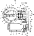
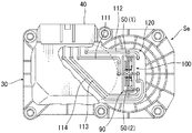
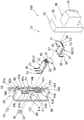
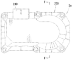
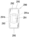
まず、電子制御式のスロットル制御装置を述べる。図1に示すように、このスロットル制御装置TCは、例えばPBT等の樹脂製のスロットルボデー1を備えている。スロットルボデー1は、ボア壁部2とモータ収容部3とを一体に有している。ボア壁部2内には、図1において紙面表裏方向に貫通するほぼ中空円筒状の吸気通路4が形成されている。なお、図示しないが、スロットルボデー1のボア壁部2の上流側にはエアクリーナが接続され、また、そのボア壁部2の下流側にはインテークマニホルドが接続されるようになっている。
First, an electronically controlled throttle control device will be described. As shown in FIG. 1, the throttle control device TC includes a
前記ボア壁部2には、前記吸気通路4を径方向に横切る金属製のスロットルシャフト6が配置されている。スロットルシャフト6の一方の端部(図1において左端部)6aは、ボア壁部2に一体形成された左側の軸受部7に軸受8を介して回転可能に支持されている。また、スロットルシャフト6の他方の端部(図1において右端部)6bは、ボア壁部2に一体形成された右側の軸受部9に軸受10を介して回転可能に支持されている。
また、スロットルシャフト6には、吸気通路4を回動によって開閉可能なスロットルバルブ12が、例えばリベット13により固定されている。スロットルバルブ12は、モータ20(後述する。)の駆動によって吸気通路4を開閉することにより、その吸気通路4を流れる吸入空気量を制御する。A
Further, a
前記左側の軸受部7には、その開口端部を密封するプラグ14が装着されている。
また、前記スロットルシャフト6の右端部6bは、前記軸受部9を貫通している。そのスロットルシャフト6の右端部6bには、例えば樹脂製の扇形ギヤからなるスロットルギヤ16が回り止めされた状態で固定されている。
また、前記スロットルボデー1と前記スロットルギヤ16との間には、バックスプリング17が設けられている。バックスプリング17は、スロットルギヤ16を前記スロットルバルブ12の常に閉じる方向へ付勢している。
なお、図示しないが、スロットルボデー1とスロットルギヤ16との間には、スロットルバルブ12を所定の閉止位置にて停止させるためのストッパ手段が設けられている。The left bearing portion 7 is provided with a
The
A
Although not shown, stopper means for stopping the
前記スロットルボデー1のモータ収容部3は、前記スロットルシャフト6の回転軸線Lに平行しかつ図1において右端面を開口するほぼ有底円筒状に形成されている。モータ収容部3内には、例えばDCモータ等からなるモータ20が挿入されている。モータ20の外郭を形成するモータケーシング21に設けられた取付フランジ22は、モータ収容部3の開口側端部に対してスクリュ23により固定されている。
The
前記モータ20の図1において右方へ突出する出力回転軸24には、例えば樹脂製のモータピニオン26が設けられている。
また、前記スロットルボデー1には、前記スロットルシャフト6の回転軸線Lに平行するカウンタシャフト27が設けられている。カウンタシャフト27には、例えば樹脂製のカウンタギヤ28が回転可能に支持されている。カウンタギヤ28は、ギヤ径の異なる大径側のギヤ部28aと小径側のギヤ部28bとを有している。大径側のギヤ部28aが前記モータピニオン26に噛み合わされ、また小径側のギヤ部28bが前記スロットルギヤ16に噛み合わされている。
なお、スロットルギヤ16とモータピニオン26とカウンタギヤ28とにより、減速ギヤ機構29が構成されている。A
The
The
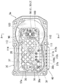
前記スロットルボデー1の側面(図1において右側面)には、例えばPBT等の樹脂製のカバー体30が結合されている。カバー体30により前記減速ギヤ機構29等が覆われている。また、スロットルボデー1とカバー体30との間には、内部の気密を保持するためのOリング(オーリング)31が介在されている。
また、スロットルボデー1に対するカバー体30の接合面には、ピン部32が突出されている。また、カバー体30に対するスロットルボデー1の接合面には、ピン部32を係入可能な受入部33が形成されている。ピン部32が受入部33内に係合されることにより、スロットルボデー1とカバー体30とが所定位置に位置決めされている。
なお、カバー体30は、本明細書でいう「樹脂成形体」に相当する。A
A
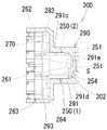
The
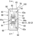
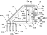
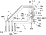
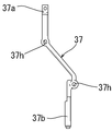
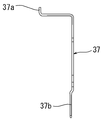
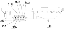
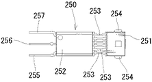
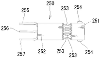
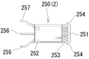
前記モータ20が有する2つのモータ端子35(図1では1個を示す。)は、前記カバー体30に設けられた中継コネクタ36にそれぞれ接続されている(図2参照。)。一方(図2において上側)の中継コネクタ36は、カバー体30にインサート成形すなわちインサートして樹脂成形された第1のプレートターミナル37のコネクタ接続端部37aに接続されている。また、他方(図2において下側)の中継コネクタ36は、カバー体30にインサート成形すなわちインサートして樹脂成形された第2のプレートターミナル38のコネクタ接続端部38aに接続されている。なお、図28は第1のプレートターミナル37を示す正面図、図29は同じく右側面図である。また、図30は第2のプレートターミナル38を示す正面図、図31は同じく右側面図である。また、各プレートターミナル37,38の外表面には、Niメッキ(図示省略)が施されている。
Two motor terminals 35 (one is shown in FIG. 1) of the
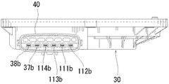
また、図2に示すように、各プレートターミナル37,38の外部接続端部37b,38bは、カバー体30の所定部位(図2において下側部)に形成されたほぼ横長四角形筒状のコネクタ部40内に突出されている(図4参照。)。また、カバー体30のコネクタ部40には、図示しない外部コネクタが接続可能となっている。また、各プレートターミナル37,38の外部接続端部37b,38b、及び、後述する各センサターミナル111,112,113,114の外部接続端部111b,112b,113b,114bには、コネクタ部40に対する外部コネクタ(図示しない。)の接続と共に、該外部コネクタ内の各端子ピン(図示省略)が接続可能になっている。
Further, as shown in FIG. 2, the external
図1において、前記モータ20は、自動車のエンジンコントロールユニットいわゆるECU等の制御手段(図示省略)によって、アクセルペダルの踏み込み量に関するアクセル信号やトラクション制御信号,定速走行信号,アイドルスピードコントロール信号に応じて駆動制御される。また、モータ20の出力回転軸24の駆動力が、モータピニオン26からカウンタギヤ28、スロットルギヤ16を介してスロットルシャフト6に伝達されることにより、スロットルバルブ12が開閉されるようになっている。
In FIG. 1, the
前記スロットルギヤ16には、ほぼ円筒状の筒状部16aが形成されている。筒状部16aは、前記スロットルシャフト6と同心状をなしている。筒状部16aの内周面には、リング状の磁性材料からなるヨーク43がスロットルシャフト6と同心状をなすようにインサート成形すなわちインサートされて樹脂成形されている。なお、スロットルギヤ16は、本明細書でいう「回転体」に相当する。
The
前記スロットルギヤ16の内側面には、前記スロットルシャフト6の回転軸線Lを間にして線対称状に配置されて磁界を発生する一対の磁石44,45が、前記ヨーク43とともにインサート成形すなわちインサートして樹脂成形されている。一対の磁石44,45は、例えばフェライト磁石からなり、ヨーク43の内側面に沿う円弧状に形成されている(図22中、二点鎖線44,45参照。)。
また、一対の磁石44,45は、両者間に発生する磁力線すなわち磁界が平行をなすように平行着磁されており、ヨーク43内の空間にほぼ平行な磁界を発生させる。なお、一対の磁石44,45を形成するフェライト磁石は、希土類磁石と比較して軟らかくて靭性が高いので円弧状に成形し易く、また材料も低コストであるので安価である。On the inner surface of the
The pair of
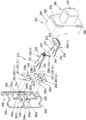
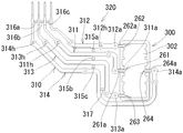
次に、前記カバー体30は、図2に示すように、前記各中継コネクタ36及び前記各プレートターミナル37,38とともにセンサターミナルアッセンブリ120(後述する。図27参照。)をインサート成形すなわちインサートして樹脂成形されている。
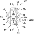
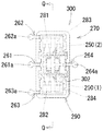
また、センサターミナルアッセンブリ120は、図26に示すように、センサアッセンブリ100とセンサターミナルユニット110とにより構成されており、そのセンサターミナルユニット110から各タイバー115a,115b,115c,116a,116b,116c(後述する。)を除去することにより形成されている(図27参照。)。
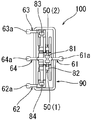
また、センサアッセンブリ100は、図18〜図20に示すように、メインターミナルアッセンブリ70とホルダ部材90とにより構成されており、そのメインターミナルアッセンブリ70から各タイバー65,66,67,68(後述する。)を除去することにより形成されている(図22〜図24参照。)。Next, as shown in FIG. 2, the
26, the
18 to 20, the
以下、説明の都合上、メインターミナルアッセンブリ70、ホルダ部材90、センサアッセンブリ100、センサターミナルユニット110、センサターミナルアッセンブリ120、カバー体30の順に詳述する。なお、図21にセンサアッセンブリ100の構成部品が分解斜視図で示されている。また、本実施例では、メインターミナルアッセンブリ70、ホルダ部材90、センサアッセンブリ100、センサターミナルユニット110、センサターミナルアッセンブリ120に関しては、カバー体30の裏面側(図1において左側)を正面側(前面側)とし、カバー体30の表面側(図1において右側)を背面側(後面側)として説明を行なうことにする。
Hereinafter, for convenience of explanation, the main
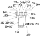
まず、メインターミナルアッセンブリ70を説明する。なお、図13はメインターミナルアッセンブリ70を示す側面図、図14は同じく背面図である。
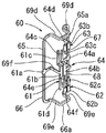
図13及び図14に示すように、メインターミナルアッセンブリ70は、2個のセンサIC50(1),50(2)と1個のメインターミナルユニット60と4個のコンデンサ81,82,83,84とにより構成されている(図21参照。)。
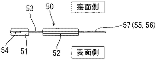
2個のセンサIC50(1),50(2)には、2個同一のセンサIC50が使用されている。図6及び図7に示すように、センサIC50は、感磁部51と、その感磁部51の後方(図6及び図7において右方)に並ぶ演算部52とを備えている。感磁部51はほぼ四角形板状をなし、また、演算部52はほぼ長四角形板状をなしている。感磁部51と演算部52とは、例えば6本の連結端子53(図7参照。)によって電気的に接続されている。感磁部51は、例えば樹脂製の外郭内に磁気抵抗素子を内蔵してなる。
また、感磁部51の外郭の左右の両側面には、金属製の位置決め片54が左右対称状(図7において上下対称状)に突出されている。この位置決め片54は、センサIC50の射出成形時における磁気抵抗素子の位置決め部材として成形型に保持されるものである。また、演算部52は、相互に平行状にかつ後方(図7において右方)へ突出する入力用接続端子55と接地用接続端子56と出力用接続端子57とを有している。
なお、センサIC50は、本明細書でいう「磁気検出装置」に相当する。First, the main
As shown in FIGS. 13 and 14, the main
Two
Further,
The
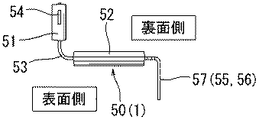
2個のセンサIC50のうち、一方のセンサIC50は、図8に示すように、前記連結端子53の折り曲げを利用して、感磁部51が裏面側(図8において上方)へほぼ90°傾倒されることにより、第1のセンサIC50(1)として形成されている。第1のセンサIC50(1)の各接続端子55,56,57は、表面側(図8において下方)へほぼ90°折り曲げられている(図21参照。)。
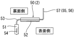
また、他方のセンサIC50は、図9に示すように、連結端子53の折り曲げを利用して、感磁部51が表面側(図9において下方)へほぼ90°傾倒されることにより、第2のセンサIC50(2)として形成されている。第2のセンサIC50(2)の各接続端子55,56,57は、裏面側(図9において上方)へほぼ90°折り曲げられている(図21参照。)。Of the two
Further, as shown in FIG. 9, the
次に、メインターミナルユニット60を説明する。なお、図10はメインターミナルユニット60を示す斜視図、図11は同じく側面図、図12は同じく背面図である。
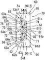
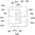
メインターミナルユニット60は、導電性を有する1枚の素材、例えば銅合金板をプレス成形することにより形成されている。図12に示すように、メインターミナルユニット60は、信号入力(以下、Vcと略記する。)用のメインターミナル61と、信号出力(以下、V1と略記する。)用のメインターミナル62と、信号出力(以下、V2と略記する。)用のメインターミナル63と、接地(以下、GNDと略記する。)用のメインターミナル64とを有している。各メインターミナル61,62,63,64のターミナル接続部61a,62a,63a,64a(後述する。)の相互間が、ほぼ四角形枠状をなすタイバー65,66,67,68により連結されたものである。Next, the main
The main
詳しくは、図12において、Vc用のメインターミナル61は、メインターミナルユニット60の右側中央部に位置するターミナル接続部61aを有している。また、V1用のメインターミナル62は、左側下部に位置するターミナル接続部62aを有している。また、V2用のメインターミナル63は、左側上部に位置するターミナル接続部63aを有している。また、GND用のメインターミナル64は、左側中央部に位置するターミナル接続部64aを有している。
そして、上側のタイバー65は、ほぼ逆U字状をなしており、右側中央部に位置するターミナル接続部61aと左側上部に位置するターミナル接続部63aとを連結している。また、下側のタイバー66は、ほぼU字状をなしており、右側中央部に位置するターミナル接続部61aと左側下部に位置するターミナル接続部62aとを連結している。また、左上側のタイバー67は、直線状をなしており、左側上部に位置するターミナル接続部63aと左側中央部に位置するターミナル接続部64aとを連結している。また、左下側のタイバー68は、左上側のタイバー67の下側に直列状に並ぶ直線状をなしており、左側下部に位置するターミナル接続部62aと左側中央部に位置するターミナル接続部64aとを連結している。Specifically, in FIG. 12, the Vc
The
図12において、前記Vc用のメインターミナル61は、前記ターミナル接続部61aの他、コンデンサ接続部61bと上側のIC端子接続部61cと下側のIC端子接続部61dとを有している。コンデンサ接続部61bは、ターミナル接続部61aの左端部に形成されている。また、上側のIC端子接続部61cは、コンデンサ接続部61bから上方へ延出されている。また、下側のIC端子接続部61dは、コンデンサ接続部61bから下方へ延出されている。
In FIG. 12, the Vc
また、前記V1用のメインターミナル62は、前記ターミナル接続部62aの他、コンデンサ接続部62bとIC端子接続部62cとを有している。コンデンサ接続部62bは、ターミナル接続部62aの右端部に形成されている。また、IC端子接続部62cは、コンデンサ接続部62bから上方へ延出されている。
The
また、前記V2用のメインターミナル63は、前記ターミナル接続部63aの他、コンデンサ接続部63bとIC端子接続部63cとを有しており、前記V1用のメインターミナル62に対して上下対称状に形成されている。すなわち、コンデンサ接続部63bは、ターミナル接続部63aの右端部に形成されている。また、IC端子接続部63cは、コンデンサ接続部63bから下方へ延出されている。
The V2
また、前記GND用のメインターミナル64は、前記ターミナル接続部64aの他、中央のコンデンサ接続部64bと上側のIC端子接続部64cと上側のコンデンサ接続部64dと下側のIC端子接続部64eと下側のコンデンサ接続部64fとを有している。中央のコンデンサ接続部64bは、ターミナル接続部64aの右端部に形成されている。また、上側のIC端子接続部64cは、コンデンサ接続部64bから上方へ延出されており、前記Vc用のメインターミナル61の上側のIC端子接続部61cと前記V2用のメインターミナル63のIC端子接続部63cとの間において平行状をなしている。また、上側のコンデンサ接続部64dは、上側のIC端子接続部64cの上端部に形成されている。また、下側のIC端子接続部64eは、中央のコンデンサ接続部64bから下方へ延出されており、前記Vc用のメインターミナル61の下側のIC端子接続部61dと前記V1用のメインターミナル62のIC端子接続部62cとの間において平行状をなしている。また、下側のコンデンサ接続部64fは、下側のIC端子接続部64eの下端部に形成されている。
The GND
しかして、前記各コンデンサ接続部61b,62b,63b,64b,64d,64f(図12参照。)は、同一平面F1(図11参照。)上に形成されている。
また、前記下側の各IC端子接続部61d,62c,64e(図12参照。)は、前記平面F1より少し後方(図11において右方)へずれた位置における同一平面F2上に形成されている。
また、前記上側の各IC端子接続部61c,63c,64c(図12参照。)は、前記平面F2よりさらに後方(図11において右方)へずれた位置における同一平面F3上に形成されている。
また、前記各ターミナル接続部61a,62a,63a,64a(図12参照。)の外端部及び各タイバー65,66,67,68は、前記平面F3よりさらに後方(図11において右方)へずれた位置における同一平面F4上に形成されている。Thus, the
Each of the lower IC
Further, the upper IC
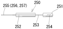
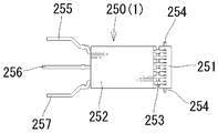
Further, the outer end portions of the
また、図10に示すように、上側のタイバー65の上辺部の中央部には、上側の各IC端子接続部61c,63c,64cの上方に位置する段違い部65aが形成されている。また、下側のタイバー66の下辺部の中央部には、前記下側の各IC端子接続部61d,62c,64eの下方に位置する段違い部66aが形成されている。また、両段違い部65a,66aは、前記各コンデンサ接続部61b,62b,63b,64b,64d,64fと同一平面F1(図11参照。)上に形成されている。
Further, as shown in FIG. 10, a stepped
上記したように、所定の平面F1,F2,F3,F4上に各部位がそれぞれ形成されるように、各部相互の連結部分には表裏方向へ折れ曲がる折曲部が形成されている。すなわち、図11において、V1用のメインターミナル62のターミナル接続部62aとコンデンサ接続部62bとは、折曲部69aを介して段違い状に形成されている。また、V2用のメインターミナル63のターミナル接続部63aとコンデンサ接続部63bとは、折曲部69bを介して段違い状に形成されている。また、GND用のメインターミナル64のターミナル接続部64aとコンデンサ接続部64bとは、折曲部69cを介して段違い状に形成されている。また、Vc用のメインターミナル61のターミナル接続部61aとコンデンサ接続部61bとは、折曲部69fを介して段違い状に形成されている(図10参照。)。また、上側のタイバー65には、左右の両折曲部69dを介して段違い部65aが形成されている。また、下側のタイバー66には、左右の両折曲部69eを介して段違い部66aが形成されている。なお、メインターミナルユニット60の外表面にはNiメッキ(図示省略)が施されている。
As described above, a bent portion that bends in the front and back direction is formed at the connecting portion of each portion so that each portion is formed on a predetermined plane F1, F2, F3, F4. That is, in FIG. 11, the
なお、各メインターミナル61,62,63,64において、各IC端子接続部61c,61d,62c,63c,64c,64eは、本明細書でいう「磁気検出装置側の接続部分」に相当する。また、各コンデンサ接続部61b,62b,63b,64b,64d,64f、及び、各IC端子接続部61c,61d,62c,63c,64c,64eは、本明細書でいう「収容側部分」に相当する。また、各ターミナル接続部61a,62a,63a,64aの外端部は、本明細書でいう「露出側部分」に相当する。そして、その収容側部分と露出側部分とが、各折曲部69a,69b,69c,69fを介して段違い状に形成されている。
In each
次に、メインターミナルアッセンブリ70を説明する。メインターミナルアッセンブリ70は、図13及び図14に示すように、前記メインターミナルユニット60に、前記各センサIC50(1),50(2)及び前記コンデンサ81,82,83,84を実装したものである(図21参照。)。すなわち、メインターミナルユニット60の表面(前面)上において、第1のセンサIC50(1)と第2のセンサIC50(2)とが対向状にかつ第1のセンサIC50(1)の感磁部51の裏側(図13において右側)に第2のセンサIC50(2)の感磁部51が重なるように配置される。
この状態で、第1のセンサIC50(1)の入力用接続端子55が、メインターミナルユニット60のVc用のメインターミナル61の下側のIC端子接続部61d上に対して、溶接(図14中の溶接部分に符号、71を付す。)により電気的に接続されている。
また、第1のセンサIC50(1)の接地用接続端子56が、メインターミナルユニット60のGND用のメインターミナル64の下側のIC端子接続部64e上に対して、溶接(図14中の溶接部分に符号、72を付す。)により電気的に接続されている。
また、第1のセンサIC50(1)の出力用接続端子57が、メインターミナルユニット60のV1用のメインターミナル62のIC端子接続部62c上に対して、溶接(図14中の溶接部分に符号、73を付す。)により電気的に接続されている。Next, the main
In this state, the
Further, the
Further, the
また、第2のセンサIC50(2)の入力用接続端子55が、メインターミナルユニット60のVc用のメインターミナル61の上側のIC端子接続部61c上に対して、溶接(図14中の溶接部分に符号、74を付す。)により電気的に接続されている。
また、第2のセンサIC50(2)の接地用接続端子56が、メインターミナルユニット60のGND用のメインターミナル64の上側のIC端子接続部64c上に対して、溶接(図14中の溶接部分に符号、75を付す。)により電気的に接続されている。
また、第2のセンサIC50(2)の出力用接続端子57が、メインターミナルユニット60のV2用のメインターミナル63のIC端子接続部63c上に対して、溶接(図14中の溶接部分に符号、76を付す。)により電気的に接続されている。
なお、前記各溶接部分71〜76の溶接には、例えばプロジェクション溶接を用いると良い。Further, the
Further, the
Further, the
For example, projection welding may be used for welding the welded
また、図14に示すように、前記メインターミナルユニット60の裏面上において、前記Vc用のメインターミナル61のコンデンサ接続部61bと前記GND用のメインターミナル64の中央のコンデンサ接続部64bとの間には、第1のコンデンサ81と第2のコンデンサ82がはんだ付けにより電気的にかつ上下に並列状に接続されている。
また、前記V1用のメインターミナル62のコンデンサ接続部62bと前記GND用のメインターミナル64の下側のコンデンサ接続部64fとの間には、第3のコンデンサ83がはんだ付けにより電気的に接続されている。
また、前記V2用のメインターミナル63のコンデンサ接続部63bと前記GND用のメインターミナル64の上側のコンデンサ接続部64dとの間には、第4のコンデンサ84がはんだ付けにより電気的に接続されている。
なお、各コンデンサ81,82,83,84は、正電荷放電対策のためのものであり、前記各センサIC50(1),50(2)に静電気による高電圧がかからないように機能する。また、本実施例のコンデンサ81,82,83,84には、チップタイプのコンデンサ、いわゆるチップコンデンサが用いられている。Further, as shown in FIG. 14, on the back surface of the main
A
Further, a
The
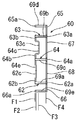
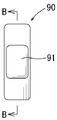
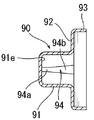
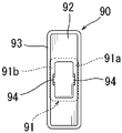
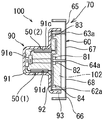
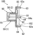
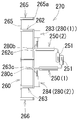
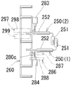
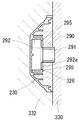
次に、ホルダ部材90を説明する。なお、図15はホルダ部材90を示す正面図、図16は図15のB−B線矢視断面図、図17はホルダ部材90を示す背面図である。
ホルダ部材90は、例えば樹脂製で、前面側を塞ぎかつ後面側を開放する有底四角筒状の中空筒部91を主体として形成されている(図16参照。)。中空筒部91の後面側(図16において右側)には、中間端板部92を介して開口を広くする膨大筒部93が連続的に形成されている。Next, the
The
前記中空筒部91の左右の両側壁部91a,91b(図17参照。)の対向する壁面の中央部には、前後方向(図16において左右方向)に延びるガイド溝94が形成されている。なお、ガイド溝94は、本明細書でいう「案内部」に相当する。
詳しくは、図16において、ガイド溝94の奥端部(中空筒部91の奥端面91e側の端部)は、各センサIC50(1),50(2)における感磁部51(図13参照。)の左右の両側面に突出された位置決め片54(図7参照。)を位置決め状態で受入可能な溝幅(図16において上下幅)の位置決め溝部94aとして形成されている。
また、ガイド溝94の位置決め溝部94aから中空筒部91の開口端面に至る部分は、位置決め溝部94aから中空筒部91の開口端面に向かって次第に溝幅(図16において上下幅)を広げるテーパ状のテーパ溝部94bとして形成されている。
また、中空筒部91の左右の両側壁部91a,91b(図17参照。)の相互間の間隔は、前記各センサIC50(1),50(2)の感磁部51及び演算部52の幅(図7において上下方向の幅)より僅かに大きい程度に形成されている。A
Specifically, in FIG. 16, the back end portion of the guide groove 94 (the end portion on the
Further, the portion from the
Further, the interval between the left and right
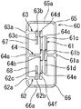
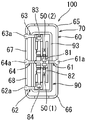
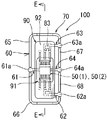
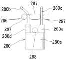
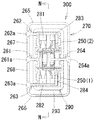
次に、センサアッセンブリ100を説明する。なお、図18はセンサアッセンブリ100の正面図、図19は図18のC−C線矢視断面図、図20はセンサアッセンブリ100の背面図である。
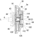
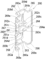
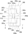
センサアッセンブリ100は、前記メインターミナルアッセンブリ70と前記ホルダ部材90とにより構成されている(図21参照。)。メインターミナルアッセンブリ70の各センサIC50(1),50(2)は、図18〜図20に示すように、前記ホルダ部材90の中空筒部91内に挿入されて収容される。このとき、第1のセンサIC50(1)の感磁部51の各位置決め片54が、ホルダ部材90の左右の各ガイド溝94のテーパ溝部94b内に嵌入されていくことにより、所定のセット位置へ向けて案内されていき、最終的に位置決め溝部94a(図16参照。)内に係入されることにより所定のセット位置に位置決めされる。これとともに、第1のセンサIC50(1)の感磁部51がホルダ部材90の中空筒部91の奥端面91eに面接触状に当接されるとともに、その演算部52がホルダ部材90の中空筒部91の下壁面91dに面接触状に当接される。Next, the
The
続いて、第2のセンサIC50(2)の感磁部51の各位置決め片54が、ホルダ部材90の左右の各ガイド溝94のテーパ溝部94b内に嵌入されていくことにより、所定のセット位置へ向けて案内されていき、最終的に位置決め溝部94a(図16参照。)内に係入されることにより所定のセット位置に位置決めされる。これとともに、第2のセンサIC50(2)の演算部52がホルダ部材90の中空筒部91の上壁面91cに面接触状に当接される。
上記のようにして、各センサIC50(1),50(2)の感磁部51の中心が、ホルダ部材90の中空筒部91の軸心線上に整合される(図19参照。)。Subsequently, each
As described above, the centers of the
前記したように、ホルダ部材90の中空筒部91内に各センサIC50(1),50(2)が収容されるにともない、そのホルダ部材90の膨大筒部93内に各センサIC50(1),50(2)の各接続端子55,56,57と各メインターミナル61,62,63,64との接続部分、及び、各コンデンサ81,82,83,84等が収容される。これとともに、各メインターミナル61,62,63,64のコンデンサ接続部61b,62b,63b,64b,64d,64f(図12参照。)がホルダ部材90の中間端板部92に当接する。また、各ターミナル接続部61a,62a,63a,64aの外端部及び各タイバー65,66,67,68が、ホルダ部材90の膨大筒部93から露出した状態におかれる。すなわち、各メインターミナル61,62,63,64における露出側部分である各ターミナル接続部61a,62a,63a,64aの外端部がホルダ部材90の開口側外部に配置されるとともに、収容側部分である各コンデンサ接続部61b,62b,63b,64b,64d,64f、及び、各IC端子接続部61c,61d,62c,63c,64c,64eがホルダ部材90内で前記露出側部分よりも底側寄りにおいて各センサIC50(1),50(2)及び各コンデンサ81,82,83,84とともに収容される。
As described above, as each sensor IC 50 (1), 50 (2) is housed in the
この状態で、前記ホルダ部材90内には、例えばディスペンサー(図示しない。)によりポッティング材102がほぼ全体的にポッティングされている。これにより、ホルダ部材90内に収容された各センサIC50(1),50(2)、及び、その各接続端子55,56,57、並びに、各コンデンサ81,82,83,84、及び、各メインターミナル61,62,63,64の収容側部分が、ポッティング材102(図19中、二点鎖線102参照。)により埋設される。
In this state, the
また、ポッティング材102には、永続性を有しかつ不用意にだれない程度の柔らかさを有する樹脂、例えばエポキシ樹脂が採用されており、熱応力、振動等から各センサIC50(1),50(2)及び各コンデンサ81,82,83,84が保護されている。
また、ポッティング材102をホルダ部材90の中空筒部91内にポッティングすることにより、各センサIC50(1),50(2)の感磁部51の歪みの発生を回避し、その歪みの発生による検出精度の低下を防止することができる。例えば、インサート成形によると、その樹脂の注入圧力によって各センサIC50(1),50(2)の感磁部51に歪みが発生し、検出精度の低下を招く不具合があるが、ポッティング材102のポッティングによればそのような不具合を解消することができる。In addition, the
Further, by potting the
前記ポッティング材102のポッティングを終了した後において、前記メインターミナルユニット60の各タイバー65,66,67,68が切断によって除去される。これにより、メインターミナルユニット60から個々に独立した各メインターミナル61,62,63,64が形成される。
上記のように構成されたセンサアッセンブリ100は、回転角センサ(符号、Seを付す。)の主体をなすものである。
なお、図22はメインターミナルユニットのメインターミナルユニットのタイバーがカットされたセンサアッセンブリ100を示す正面図、図23は図22のD−D線矢視断面図、図24は同センサアッセンブリ100の背面図である。After the potting of the
The
22 is a front view showing the
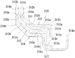
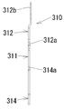
次に、センサターミナルユニット110を説明する。図25はセンサターミナルユニット110の正面図である。
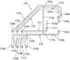
センサターミナルユニット110は、導電性を有する1枚の素材、例えば銅合金板をプレス成形することにより形成されている。センサターミナルユニット110は、Vc用のセンサターミナル111と、V1用のセンサターミナル112と、V2用のセンサターミナル113と、GND用のセンサターミナル114とを有している。そして、隣り合うセンサターミナル111,112,113,114の相互間が、各タイバー115a,115b,115c、116a,116b,116cにより連結されたものである。
詳しくは、図25において、センサターミナルユニット110のターミナル接続側となる右側の下部では、Vc用のセンサターミナル111と、そのセンサターミナル111の下方近くにV1用のセンサターミナル112が平行状に並んでいる。また、その右側上部では、GND用のセンサターミナル114と、そのセンサターミナル114の下方近くにV2用のセンサターミナル113が平行状に並んでいる。各タイバー115a,115b,115cは上下方向に直列状に並ぶ直線状をなしている。上側のタイバー115aは、GND用のセンサターミナル114とV2用のセンサターミナル113とを連結している。また、中央のタイバー115bは、V2用のセンサターミナル113とVc用のセンサターミナル111とを連結している。また、下側のタイバー115cは、V2用のセンサターミナル113とV1用のセンサターミナル112とを連結している。Next, the
The
Specifically, in FIG. 25, in the lower part on the right side that is the terminal connection side of the
また、センサターミナルユニット110の外部接続側となる左側の下部では、GND用のセンサターミナル114とV2用のセンサターミナル113とVc用のセンサターミナル111とV1用のセンサターミナル112とが左右方向に平行状に並んでいる。各タイバー115a,115b,115cは左右方向に直列状に並ぶ直線状をなしている。左側のタイバー116aは、GND用のセンサターミナル114とV2用のセンサターミナル113とを連結している。また、中央のタイバー116bは、V2用のセンサターミナル113とVc用のセンサターミナル111とを連結している。また、右側のタイバー116cは、Vc用のセンサターミナル111とV1用のセンサターミナル112とを連結している。
In addition, in the lower part on the left side that is the external connection side of the
図25において、Vc用のセンサターミナル111は、その一端部すなわちターミナル接続側となる右端部に形成されたターミナル接続端部111aと、その他端部すなわち外部接続側となる左端部に形成された外部接続端部111bとを有している。ターミナル接続端部111aは、前記センサアッセンブリ100におけるVc用のメインターミナル61のターミナル接続部61a(図22参照。)と接続可能に形成されている。また、外部接続端部111bは、図示しない外部コネクタの当該端子ピンと接続可能に形成されている。
また、V1用のセンサターミナル112は、その一端部すなわちターミナル接続側となる右端部に形成されたターミナル接続端部112aと、その他端部すなわち外部接続側となる左端部に形成された外部接続端部112bとを有している。ターミナル接続端部112aは、センサアッセンブリ100におけるホルダ部材90の下側部を取り巻くように延びており、センサアッセンブリ100におけるV1用のメインターミナル62のターミナル接続部62a(図22参照。)と接続可能に形成されている。また、外部接続端部112bは、図示しない外部コネクタの当該端子ピンと接続可能に形成されている。
また、V2用のセンサターミナル113は、その一端部すなわちターミナル接続側となる右端部に形成されたターミナル接続端部113aと、その他端部すなわち外部接続側となる左端部に形成された外部接続端部113bとを有している。ターミナル接続端部113aは、センサアッセンブリ100におけるホルダ部材90の上側部を取り巻くように延びており、センサアッセンブリ100におけるV2用のメインターミナル63のターミナル接続部63a(図22参照。)と接続可能に形成されている。また、外部接続端部113bは、図示しない外部コネクタの当該端子ピンと接続可能に形成されている。
また、GND用のセンサターミナル114は、その一端部すなわちターミナル接続側となる右端部に形成されたターミナル接続端部114aと、その他端部すなわち外部接続側となる左端部に形成された外部接続端部114bとを有している。ターミナル接続端部114aは、センサアッセンブリ100におけるホルダ部材90の上側部を取り巻くように延びており、センサアッセンブリ100におけるGND用のメインターミナル64のターミナル接続部64a(図22参照。)と接続可能に形成されている。また、外部接続端部114bは、図示しない外部コネクタの当該端子ピンと接続可能に形成されている。In FIG. 25, the
The
Further, the
The
また、前記各センサターミナル111,112,113,114の外部接続端部111b,112b,113b,114bは、右から左方へ外部接続端部112b、外部接続端部111b、外部接続端部113b、外部接続端部114bの順で平行状に並んだ状態で下方へ延出されている。なお、センサターミナルユニット110の外表面にはNiメッキ(図示省略)が施され、各ターミナル接続端部111a,112a,113a,114aにはAuメッキが施されている。また、各センサターミナル111,112,113,114には、適数個の貫通孔111h,112h,113h,114hがそれぞれ形成されている(図25参照。)。各貫通孔111h,112h,113h,114hには、カバー体30(後述する。)の樹脂成形時における金型の位置決めピン(図示しない。)が嵌合されることにより、金型に各センサターミナル111,112,113,114が位置決めされるようになっている。これと同様に、各プレートターミナル37,38にも同様に、適数個の貫通孔37h、38hがそれぞれ形成されている(図28、図30参照。)。
Further, the external connection ends 111b, 112b, 113b, 114b of the
次に、センサターミナルアッセンブリ120を説明する。図26はセンサターミナルアッセンブリの正面図である。
センサターミナルアッセンブリ120は、前記センサアッセンブリ100(図22〜図24参照。)を前記センサターミナルユニット110(図25参照。)に実装したものである。
すなわち、センサターミナルユニット110のVc用のセンサターミナル111のターミナル接続端部111a上に、センサアッセンブリ100のVc用のメインターミナル61のターミナル接続部61aが溶接(溶接部分に符号、121を付す。)により電気的に接続されている。
また、センサターミナルユニット110のV1用のセンサターミナル112のターミナル接続端部112a上に、センサアッセンブリ100のV1用のメインターミナル62のターミナル接続部62aが溶接(溶接部分に符号、122を付す。)により電気的に接続されている。
また、センサターミナルユニット110のV2用のセンサターミナル113のターミナル接続端部113a上に、センサアッセンブリ100のV2用のメインターミナル63のターミナル接続部63aが溶接(溶接部分に符号、123を付す。)により電気的に接続されている。
また、センサターミナルユニット110のGND用のセンサターミナル114のターミナル接続端部114a上に、センサアッセンブリ100のGND用のメインターミナル64のターミナル接続部64aが溶接(溶接部分に符号、124を付す。)により電気的に接続されている。
なお、前記各溶接部分121,122,123,124の溶接には、例えばプロジェクション溶接を用いると良い。Next, the
The
That is, the
Further, the
Further, the
The
For example, projection welding may be used for welding the welded
前記溶接後において、前記センサターミナルユニット110の各タイバー115a,115b,115c、116a,116b,116cが切断によって除去される。これにより、図27に示すように、個々に独立したセンサターミナル111,112,113,114が形成される。このように形成されたセンサターミナル111,112,113,114は、本明細書でいう「サブターミナル」及び「外部ターミナル」に相当する。なお、図27は、タイバーがカットされたセンサターミナルアッセンブリ120の正面図を示している。
After the welding, the tie bars 115a, 115b, 115c, 116a, 116b, and 116c of the
次に、カバー体30を説明する。カバー体30は、図2に示すように、前記センサターミナルアッセンブリ120(図27参照。)及び前記各プレートターミナル37,38(図28〜図31参照。)並びに前記各中継コネクタ36がインサート成形すなわちインサートして樹脂成形されている。
また、カバー体30の樹脂成形時において、センサターミナルアッセンブリ120のホルダ部材90を取り巻くカバー体30の樹脂部は、ホルダ部材90の中空筒部91の中央部におけるばり止め面126においてばり止めされている。なお、「ばり止め」は、「ばり切り」とも呼ばれており、樹脂成形時において、樹脂部で埋設されない部分(本実施例では、ホルダ部材90の中空筒部91の底側半部(図3において左半部が相当する。))を露出するように、その露出部分を嵌合する側の金型によって、露出部分側への樹脂の流れを堰き止めることである。そして、前記露出部分を嵌合する側の金型によって形成されかつ露出部分を取り巻く樹脂部の端面を「ばり止め面」と称している。Next, the
Further, at the time of resin molding of the
また、図2に示すように、前記各センサターミナル111,112,113,114の各外部接続端部111b,112b,113b,114bは、前記各プレートターミナル37,38の各外部接続端部37b,38bとともに、前記カバー体30のコネクタ部40内に突出されている(図4参照。)。
また、各外部接続端部37b,38b,111b,112b,113b,114bは、図4において左右方向に列状に並んでいる。なお、本実施例の場合、図4において左から右へ順に、外部接続端部38b,37b,114b,113b,111b,112bが並んでいる。
また、各外部接続端部37b,38b,111b,112b,113b,114bには、前にも述べたように、コネクタ部40に接続される外部コネクタ(図示しない。)の各端子ピン(図示省略)が接続可能になっている。
上記のように、センサアッセンブリ100に、各センサターミナル111,112,113,114及びカバー体30並びに各中継コネクタ36、各プレートターミナル37,38を備えることにより、回転角センサSeが構成されている(図2参照。)。In addition, as shown in FIG. 2, the external connection ends 111b, 112b, 113b, 114b of the
Further, the external
Further, as described above, each external
As described above, the
上記のように構成されたカバー体30が、図1に示すように、前記スロットルボデー1の側面(図1において右側面)に結合されることにより、スロットル制御装置TCが完成する。これとともに、回転角センサSeのホルダ部材90の中空筒部91は、前記ヨーク43の軸線すなわちスロットルシャフト6の回転軸線L上にほぼ同心状にかつ両磁石44,45の相互間に所定の間隔を隔てた位置に配置される。
また、回転角センサSeの各センサIC50(1),50(2)の感磁部51は、磁石44,45間においてほぼ同心状にかつその感磁部51の四角形面が前記スロットルシャフト6の回転軸線Lに直交するように配置されることにより、前記一対の磁石44,45の間に発生する磁界の方向を精度良く検出する。As shown in FIG. 1, the
Further, the
しかして、前記各センサIC50(1),50(2)(図3参照。)は、感磁部51内の磁気抵抗素子からの出力を演算部52において計算して、前記ECU等の制御手段に磁界の方向に応じた出力信号を出力することにより、磁界の強度に依存することなく、磁界の方向を検出できるように構成されている。
また、センサIC50を2個使用することにより、精度の高い検出が行なえるとともに、仮にどちらか1個が故障したとしても残りの1個での磁界の方向を検出が行なえる。Thus, each of the sensor ICs 50 (1), 50 (2) (see FIG. 3) calculates an output from the magnetoresistive element in the
Further, by using two
上記したスロットル制御装置TC(図1参照。)において、エンジンが始動されると、ECU等の制御手段によってモータ20が駆動制御される。これにより、前にも述べたように、減速ギヤ機構29を介してスロットルバルブ12が開閉される結果、スロットルボデー1の吸気通路4を流れる吸入空気量が制御される。そして、スロットルシャフト6の回転にともなってスロットルギヤ16及びヨーク43並びに両磁石44,45が回転すると、その回転角に応じて各センサIC50(1),50(2)(図3参照。)に交差する磁界の方向が変化する。これにより、各センサIC50(1),50(2)の出力信号が変化する。各センサIC50(1),50(2)の出力信号が出力される前記ECU等の制御手段(図示省略)では、各センサIC50(1),50(2)の出力信号に基づいて、スロットルシャフト6の回転角すなわちスロットルバルブ12の開度が算出される。
In the throttle control device TC (see FIG. 1), when the engine is started, the
また、前記ECU等の制御手段(図示省略)は、前記回転角センサSeの各センサIC50(1),50(2)から出力されかつ一対の磁石44,45の磁気的物理量としての磁界の方向によって検出されたスロットル開度と、車速センサ(図示省略)によって検出された車速と、クランク角センサによるエンジン回転数と、アクセルペダルセンサ、O2センサ、エアフローメータ等のセンサからの検出信号等に基づいて、燃料噴射制御、スロットルバルブ12の開度の補正制御、オートトランスミッションの変速制御等の、いわゆる制御パラメータを制御する。Further, the control means (not shown) such as the ECU is a direction of the magnetic field output from each sensor IC 50 (1), 50 (2) of the rotation angle sensor Se and as a magnetic physical quantity of the pair of
上記したスロットル制御装置TCに備えた回転角センサSe(図2及び図3参照。)によると、回転体であるスロットルギヤ16の回転角を検出する各センサIC50(1),50(2)の各接続端子55,56,57が各メインターミナル61,62,63,64に接続されている。したがって、従来必要とされた高価なプリント基板に比べて、安価なメインターミナル61,62,63,64を用いることにより、コストを低減することができる。
また、各センサIC50(1),50(2)、及び、各メインターミナル61,62,63,64の各センサIC50(1),50(2)側の接続部分をホルダ部材90に保持するため、各センサIC50(1),50(2)と各配線用ターミナル(本明細書でいうメインターミナルとサブターミナル(センサターミナル)とが一体に形成されたターミナルが相当する。)とを樹脂一体成形する金型を不要とすることができる。これにより、設備費を削減し、コストを低減することができる。According to the rotation angle sensor Se (see FIGS. 2 and 3) provided in the throttle control device TC described above, the sensor ICs 50 (1) and 50 (2) for detecting the rotation angle of the
In addition, in order to hold the sensor ICs 50 (1), 50 (2) and the connection portions of the
また、各センサIC50(1),50(2)と各メインターミナル61,62,63,64とホルダ部材90とをアッシー化したセンサアッセンブリ100(図22〜図24参照。)を構成したことにより、各センサIC50(1),50(2)及び各メインターミナル61,62,63,64の取り扱いに有利である。また、プリント基板を用いる場合に比べて、構造が簡略化されるので、センサアッセンブリを小型化することができる。これにより、設備費を削減し、コストを低減することができる。
Further, the sensor assembly 100 (see FIGS. 22 to 24) in which the sensor ICs 50 (1) and 50 (2), the
また、各センサIC50(1),50(2)の各接続端子55,56,57と各メインターミナル61,62,63,64とが溶接(図14における溶接部分71〜76参照。)により接続されている。このため、各センサIC50(1),50(2)の各接続端子55,56,57と各メインターミナル61,62,63,64との接続強度が高まるので、温度サイクルの繰り返しでの断線を防止あるいは低減することができる。さらには、回転角センサSeの信頼性を向上することができる。
Further, the
また、ホルダ部材90の左右の両側壁部91a,91bの対向する内壁面に設けた位置決め溝部94a及びテーパ溝部94b(図16参照。)を有するガイド溝94により、各センサIC50(1),50(2)の挿入時に、そのセンサIC50(1),50(2)の感磁部51の両位置決め片54を所定のセット位置に案内することができる。
詳しくは、ホルダ部材90のガイド溝94の開口側端部にテーパ溝部94b(図16参照。)を備えているので、テーパ溝部94bに対する位置決め片54の係合可能範囲を広くとることができる。このため、各センサIC50(1),50(2)の感磁部51の位置決め片54を位置決め溝部94aに容易に係合することができる。その後、位置決め片54がテーパ溝部94bにより位置決め溝部94aに向けて案内されていき、最終的に位置決め片54が位置決め溝部94aの所定位置において位置決めされる。このため、各センサIC50(1),50(2)をホルダ部材90内の所定のセット位置に容易にかつ精度良く組付けることができる(図19参照。)。これとともに、各センサIC50(1),50(2)の位置ずれを防止あるいは低減することができる。このため、各センサIC50(1),50(2)の組付性を向上するとともに、回転角センサSeの検出精度及び信頼性を向上することができる。Further, each sensor IC 50 (1), 50 is provided by a
Specifically, since the tapered
また、ホルダ部材90内に、各センサIC50(1),50(2)、及び、各センサIC50(1),50(2)の各接続端子55,56,57と各メインターミナル61,62,63,64との接続部分を覆う柔軟性を有するポッティング材102がポッティングされている(図19参照。)。このため、電気的な導通部分に対する水気の侵入を防止することができ、短絡すなわちショート、マイグレーションの発生を防止あるいは低減することができる。さらに、ポッティング材102が柔軟性を有するので、熱応力、振動等から各センサIC50(1),50(2)を保護することができる。さらに、ポッティング時に各センサIC50(1),50(2)に余分な圧力が加わらないので、その圧力による各センサIC50(1),50(2)の特性変化を回避することができる。このような理由により、回転角センサSeの信頼性を向上することができる。
また、プリント基板を用いた場合には、そのプリント基板を覆うために多量のポッティング材102が必要となるのに比べて、ホルダ部材90で囲繞された空間内において各センサIC50(1),50(2)の各接続端子55,56,57と各メインターミナル61,62,63,64との接続部分をポッティング材102で覆うすなわちモールドすることにより、ポッティング材102の使用量を少なくし、ポッティング材102にかかる材料費を低減することができる。
また、各センサIC50(1),50(2)と各センサターミナル111,112,113,114とを樹脂一体成形(1次成形)する場合と異なり、樹脂成形のための金型にかかる設備費を削減し、コストを低減することができる。また、樹脂成形の成形圧による各センサIC50(1),50(2)及び各メインターミナル61,62,63,64の位置ずれ、各センサIC50(1),50(2)の各接続端子55,56,57及び各メインターミナル61,62,63,64の変形等による成形不良を防止あるいは低減することができる。
また、ポッティング材102としてのエポキシ樹脂は、シリコン系UV樹脂に比べて安価であるため、コストアップを抑えることができる。なお、ポッティング材102として、シリコン系UV樹脂を採用することができる。Also, in the
Further, when a printed circuit board is used, each sensor IC 50 (1), 50 in the space surrounded by the
Unlike the case where the sensor ICs 50 (1), 50 (2) and the
Moreover, since the epoxy resin as the
また、正電荷放電対策のための各コンデンサ81,82,83,84が、各メインターミナル61,62,63,64の相互間に接続されかつポッティング材102により覆われている(図19参照。)。このため、柔軟性を有するポッティング材102により、熱応力、振動等から各コンデンサ81,82,83,84を保護することができる。また、ポッティング時に各コンデンサ81,82,83,84に余分な圧力が加わらないので、その圧力による各コンデンサ81,82,83,84の断線、破壊等を回避することができる。これにより、回転角センサSeの信頼性を向上することができる。
Further, each
また、各メインターミナル61,62,63,64における各センサIC50(1),50(2)及び各コンデンサ81,82,83,84を接続する収容側部分と、各センサターミナル111,112,113,114を接続する露出側部分とを段違い状に形成して、露出側部分をホルダ部材90の開口側に配置し、収容側部分をホルダ部材90内で露出側部分よりも底側寄りにおいて各センサIC50(1),50(2)及び各コンデンサ81,82,83,84とともに収容している。このため、各センサIC50(1),50(2)及び各コンデンサ81,82,83,84を含む電気的な導通部分に対する防水性が必要な部位に対するポッティング材102のポッティングを容易にかつ確実に行なうことができる。これにより、電気的な導通部分におけるショートの発生を防止あるいは低減することができる。
In addition, a housing-side portion for connecting the sensor ICs 50 (1), 50 (2) and the
また、センサアッセンブリ100、及び、センサアッセンブリ100の各メインターミナル61,62,63,64のターミナル接続部61a,62a,63a,64aに接続されかつ外部コネクタの端子ピン(図示しない。)を接続可能な各センサターミナル111,112,113,114をインサートして樹脂成形されたカバー体30(図2及び図3参照。)を備えている。このため、カバー体30に対してセンサアッセンブリ100及び各センサターミナル111,112,113,114を容易に配置することができる。
また、センサアッセンブリ100の各メインターミナル61,62,63,64と各センサターミナル111,112,113,114とを接続する構成であるので、外部コネクタの接続位置及び接続方向(すなわち、コネクタ部40の形成位置及び向き)並びに各センサターミナル111,112,113,114の配線経路等が異なる形式のカバー体30に対してセンサアッセンブリ100を共通化することができる。The
Further, since each
また、カバー体30(図2及び図3参照。)に各センサターミナル111,112,113,114及び各プレートターミナル37,38が樹脂成形により一体化されているので、カバー体30の所定位置に各センサターミナル111,112,113,114及び各プレートターミナル37,38を精度良く配置することができる。
Moreover, since each sensor terminal 111,112,113,114 and each
また、上記した回転角センサSeの製造方法は、導電性を有する1枚の素材をプレス成形することにより、各メインターミナル61,62,63,64が各タイバー65,66,67,68を介して連結されたメインターミナルユニット60を形成する工程と、
前記メインターミナルユニット60に前記各センサIC50(1),50(2)の各接続端子55,56,57を接続してメインターミナルアッセンブリ70を形成する工程と、
前記ホルダ部材90内に、前記メインターミナルアッセンブリ70の前記各センサIC50(1),50(2)及び前記各メインターミナル61,62,63,64の各センサIC50(1),50(2)側の接続部分を収容した状態に配置する工程と、
前記メインターミナルユニット60から前記各タイバー65,66,67,68を除去する工程と
を備えている。
したがって、この回転角センサSeの製造方法によると、1枚の素材のプレス成形によりメインターミナルユニット60を形成することにより、各メインターミナル61,62,63,64を精度良く形成することができる。
また、メインターミナルユニット60に各センサIC50(1),50(2)の各接続端子55,56,57を接続してメインターミナルアッセンブリ70を形成することにより、各メインターミナル61,62,63,64に各センサIC50(1),50(2)の各接続端子55,56,57を精度良く接続することができる。
また、ホルダ部材90内に、メインターミナルアッセンブリ70の各センサIC50(1),50(2)及び各メインターミナル61,62,63,64の各センサIC50(1),50(2)側の接続部分を収容した状態に配置することにより、各センサIC50(1),50(2)をメインターミナルアッセンブリ70に支持した状態でホルダ部材90内に所定位置に容易に配置することができる。
また、メインターミナルユニット60から各タイバー65,66,67,68を除去することにより、個々に独立した各メインターミナル61,62,63,64を容易に形成することができる。
したがって、回転角センサSeを合理的に製造することができる。Further, in the manufacturing method of the rotation angle sensor Se described above, each
Connecting the
Inside the
Removing the tie bars 65, 66, 67, 68 from the main
Therefore, according to the method of manufacturing the rotation angle sensor Se, the
Further, by connecting the
In addition, in the
Further, by removing the tie bars 65, 66, 67, and 68 from the main
Therefore, the rotation angle sensor Se can be reasonably manufactured.
また、前記スロットル制御装置TC(図1参照。)によると、前記回転角センサSeを備えて、スロットルバルブ12の開度を検出するように構成されている。したがって、コストを低減することのできる回転角センサSeを備えたスロットル制御装置TCを提供することができる。
In addition, according to the throttle control device TC (see FIG. 1), the rotation angle sensor Se is provided to detect the opening degree of the
また、回転角センサSeの各センサIC50(1),50(2)により、スロットルシャフト6に配置された一対の磁石44,45の間に発生する磁界の方向を検出し、各センサIC50(1),50(2)の出力に基づいてスロットルバルブ12の開度を検出する(図3及び図4参照。)。したがって、各センサIC50(1),50(2)が磁界の方向を検出することにより、例えば、スロットルシャフト6の位置ずれにともなう磁石44,45の位置ずれや、磁石44,45の温度特性による磁界の強度の変化等にほとんど影響されない。なお、スロットルシャフト6の位置ずれとは、各センサIC50(1),50(2)に対する相対的な位置ずれであって、スロットルシャフト6の組付誤差、スロットルボデー1とカバー体30の熱膨張差、スロットルシャフト6や軸受8,10の摩耗によるがたつきや、両磁石44,45をインサート成形した樹脂(スロットルギヤ16)の熱膨張等によって発生する。
このため、各センサIC50(1),50(2)により磁界の方向を精度良く検出することができ、これによりスロットルバルブ12の開度の検出精度を向上することができる。このことは、スロットルボデー1が加工精度の悪い樹脂製の場合に、特に有利である。また、スロットルボデー1とカバー体30とが異なる材料の場合、例えばスロットルボデー1が金属製で、カバー体30が樹脂製である場合にも有利である。The direction of the magnetic field generated between the pair of
For this reason, the direction of the magnetic field can be accurately detected by the sensor ICs 50 (1) and 50 (2), and thereby the detection accuracy of the opening degree of the
また、スロットルシャフト6に配置された一対の磁石44,45は、スロットルギヤ16に配置されかつ回転軸線Lをほぼ中心とするリング状の磁性材料からなるヨーク43の内側面に配置され、かつ相互間に発生する磁界が平行をなすように平行着磁されている(図4参照。)。したがって、一対の磁石44,45及びヨーク43を含む磁気回路が形成され、かつ一対の磁石44,45が、平行着磁されることにより、磁石44,45の間に発生する磁界がほとんど平行となる。このため、各センサIC50(1),50(2)による磁界の方向の検出精度を一層向上することができる。
A pair of
[実施例2]
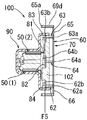
本発明の実施例2を説明する。本実施例は、前記実施例1におけるメインターミナルアッセンブリ70(図13及び図14参照。)の変更例を説明するものであるから、重複する説明は省略し、変更部分について説明する。なお、図32はセンサアッセンブリ100を示す正面図、図33は図32のE−E線矢視断面図、図34はセンサアッセンブリ100を示す背面図である。
図32〜図34に示すように、本実施例のメインターミナルアッセンブリ70におけるメインターミナルユニット60には、各コンデンサ81,82,83,84が各センサIC50(1),50(2)の接続側と同一側すなわち表面側に装着されている。このため、メインターミナルユニット60の各メインターミナル61,62,63,64が、前記実施例1における各コンデンサ81,82,83,84の裏側の平面F5上に各コンデンサ接続部61b,62b,63b,64b,64d,64fを配置するように折り曲げ形成されている。
上記のように構成された実施例2によっても、前記実施例1と同様の作用・効果が得られる。
さらに、各コンデンサ81,82,83,84が、各メインターミナル61,62,63,64における各センサIC50(1),50(2)の接続側と同一側に配置されていることにより、各メインターミナル61,62,63,64に対して各センサIC50(1),50(2)と各コンデンサ81,82,83,84を容易に配置することができる。[Example 2]
A second embodiment of the present invention will be described. Since the present embodiment describes a modified example of the main terminal assembly 70 (see FIGS. 13 and 14) in the first embodiment, the overlapping description will be omitted and the modified portion will be described. 32 is a front view showing the
As shown in FIGS. 32 to 34, in the main
According to the second embodiment configured as described above, the same operation and effect as the first embodiment can be obtained.
Furthermore, each
[実施例3]
本発明の実施例3を説明する。本実施例では、前記実施例1における回転角センサSeの変更例を説明するものであるから、重複する説明は省略し、変更部分について説明する。
図35に示すように、回転角センサSeが備えるカバー体(符号、230を付す。)は、前記実施例1と同様、スロットル制御装置TCのスロットルボデー1の側面に結合されるようになっている。なお、カバー体230は、本明細書でいう「樹脂成形体」に相当する。[Example 3]
A third embodiment of the present invention will be described. In the present embodiment, a modification example of the rotation angle sensor Se in the first embodiment will be described. Therefore, a redundant description will be omitted, and the changed portion will be described.
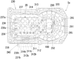
As shown in FIG. 35, the cover body (denoted by reference numeral 230) provided in the rotation angle sensor Se is coupled to the side surface of the
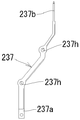
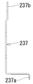
前記スロットルボデー1に組込まれたモータ20が有する2つのモータ端子35(図35では1個を示す。)は、前記カバー体230に設けられた中継コネクタ236にそれぞれ接続されている(図38参照。)。一方(図38において上側)の中継コネクタ236は、カバー体230にインサート成形すなわちインサートして樹脂成形された第1のプレートターミナル237(図79及び図80参照。)のコネクタ接続端部237aに接続されている。また、他方(図38において下側)の中継コネクタ236は、カバー体230にインサート成形すなわちインサートして樹脂成形された第2のプレートターミナル238(図81及び図82参照。)のコネクタ接続端部238aに接続されている。なお、図79は第1のプレートターミナル237を示す正面図、図80は同じく右側面図である。また、図81は第2のプレートターミナル238を示す正面図、図82は同じく右側面図である。また、各プレートターミナル237,238の外表面には、Niメッキ(図示省略)が施されている。
Two motor terminals 35 (one is shown in FIG. 35) of the
また、図38に示すように、各プレートターミナル237,238の外部接続端部237b,238bは、カバー体230の所定部位(図38において下側部)に形成されたほぼ横長四角形筒状のコネクタ部240内に突出されている(図37参照。)。また、カバー体230のコネクタ部240には、図示しない外部コネクタが接続可能となっている。また、各プレートターミナル237,238の外部接続端部237b,238b、及び、後述する各センサターミナル311,312,313,314の外部接続端部311b,312b,313b,314bには、コネクタ部240に対する外部コネクタ(図示しない。)の接続と共に、該外部コネクタ内の各端子ピン(図示省略)が接続可能になっている。
As shown in FIG. 38, the external connection ends 237b and 238b of the
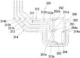
前記カバー体230は、図38に示すように、前記各中継コネクタ236及び前記各プレートターミナル237,238とともにセンサターミナルアッセンブリ320(後述する。図78参照。)をインサート成形すなわちインサートして樹脂成形されている。
また、センサターミナルアッセンブリ320は、図77に示すように、センサアッセンブリ300とセンサターミナルユニット310とにより構成されており、そのセンサターミナルユニット310から各タイバー315a,315b,315c,316a,316b,316c(後述する。)を除去することにより形成されている(図78参照。)。
また、センサアッセンブリ300は、図69及び図70に示すように、メインターミナルアッセンブリ270とホルダ部材290とにより構成されており、そのメインターミナルアッセンブリ270から各タイバー265,266,267,268(後述する。)を除去することにより形成されている(図73及び図74参照。)。As shown in FIG. 38, the
77, the
69 and 70, the
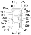
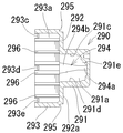
以下、説明の都合上、メインターミナルアッセンブリ270、ホルダ部材290、センサアッセンブリ300、センサターミナルユニット310、センサターミナルアッセンブリ320、カバー体230の順に詳述する。なお、図68にセンサアッセンブリ300の構成部品が分解斜視図で示されている。また、本実施例では、メインターミナルアッセンブリ270、ホルダ部材290、センサアッセンブリ300、センサターミナルユニット310、センサターミナルアッセンブリ320に関しては、カバー体230の表面側(図35において右側)を正面側(前面側)とし、カバー体230の裏面側(図35において左側)を背面側(後面側)として説明を行なうことにする。
Hereinafter, for convenience of explanation, the main
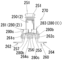
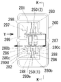
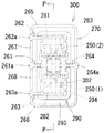
まず、メインターミナルアッセンブリ270を説明する。なお、図57はメインターミナルアッセンブリ270を示す正面図、図58は図57のH−H線矢視断面図、
図59は図57のI−I線矢視断面図、図60は図57のJ−J線矢視断面図が示されている。
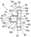
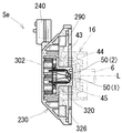
図57〜図60に示すように、メインターミナルアッセンブリ270は、2個のセンサIC250(1),250(2)と1個のメインターミナルユニット260と4個のコンデンサ281,282,283,284とにより構成されている(図68参照。)。
2個のセンサIC250(1),250(2)には、2個同一のセンサIC250が使用されている。図40〜図42に示すように、センサIC250は、前記実施例1(図6及び図7参照。)と同じもので、感磁部251と、その感磁部251の前方(図40〜図42において左方)に6本の連結端子253を介して並ぶ演算部252とを備えている。本実施例の感磁部251は、樹脂製の外郭内に磁気抵抗素子を内蔵しており、その外郭の左右の両側面に金属製の位置決め片254が左右対称状(図40において上下対称状)に突出されている。また、演算部252は、相互に平行状にかつ前方(図40〜図42において左方)へ突出する入力用接続端子255と接地用接続端子256と出力用接続端子257とを有している。なお、センサIC250は、本明細書でいう「磁気検出装置」に相当する。First, the main
59 is a cross-sectional view taken along the line II of FIG. 57, and FIG. 60 is a cross-sectional view taken along the line JJ of FIG.
As shown in FIGS. 57 to 60, the main
Two
2個のセンサIC250のうち、一方のセンサIC250は、図43及び図44に示すように、前記連結端子253の折り曲げを利用して、感磁部251が表面側(図43において上方)へほぼ90°傾倒されることにより、第1のセンサIC250(1)として形成されている。第1のセンサIC250(1)の両側に位置する各接続端子255,257の先端部は、相互に平行をなすように側方へ拡開されており、中央に位置する接続端子256に対する間隔が拡大されている(図44参照。)。
また、他方のセンサIC250は、図45及び図46に示すように、連結端子253の折り曲げを利用して、感磁部251が裏面側(図46において下方)へほぼ90°傾倒されることにより、第2のセンサIC250(2)として形成されている。第2のセンサIC250(2)の両側に位置する各接続端子255,257の先端部は、第1のセンサIC250(1)と同様に、相互に平行をなすように側方へ拡開されており、中央に位置する接続端子256に対する間隔が拡大されている(図45参照。)。Of the two
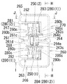
Further, as shown in FIGS. 45 and 46, the
次に、前記各コンデンサ281,282,283,284を説明する。各コンデンサ281,282,283,284(図68参照。)には、同一のコンデンサ280が用いられている。図52に示すように、コンデンサ280は、コンデンサ本体280aと、そのコンデンサ本体280a上に並ぶ左右2本のリード280b,280cを備えている。各リード280b,280cの基端部は、コンデンサ本体280aの外殻の上面に一体形成された支持部280d,280eによって支持されている。なお、各コンデンサ281,282,283,284(図68参照。)は、前記実施例1における各コンデンサ81,82,83,84と同様、正電荷放電対策のためのものであり、前記各センサIC250(1),250(2)に静電気による高電圧がかからないように機能する。
Next, the
前記4個のコンデンサ281,282,283,284のうち、2個のコンデンサ282,283には同一のコンデンサ280(1)(図53及び図54参照。)が用いられ、残りの2個のコンデンサ281,284には同一のコンデンサ280(2)(図55及び図56参照。)が用いられている。
一方のコンデンサ280(1)は、図53及び図54に示すように、左側のリード280bが左方へ斜めに傾倒されており、かつ両リード280b,280cの先端部が前方(図54において左方)へ平行状に折り曲げられている。
また、他方のコンデンサ280(2)は、図55及び図56に示すように、右側のリード280cが右方へ斜めに傾倒されており、かつ両リード280b,280cの先端部が前方(図54において左方)へ平行状に折り曲げられている。Of the four
As shown in FIGS. 53 and 54, one capacitor 280 (1) has the
In the other capacitor 280 (2), as shown in FIGS. 55 and 56, the
次に、メインターミナルユニット260を説明する。なお、図47はメインターミナルユニット260の斜視図、図48は同じく展開図である。また、図49はメインターミナルユニットを示す正面図、図50は同じく右側面図、図51は図49のG−G線矢視断面図である。
メインターミナルユニット260は、導電性を有する1枚の素材、例えば銅合金板をプレス成形することにより形成されている。図48に示すように、メインターミナルユニット260は、信号入力(以下、Vcと略記する。)用のメインターミナル261と、信号出力(以下、V1と略記する。)用のメインターミナル262と、信号出力(以下、V2と略記する。)用のメインターミナル263と、接地(以下、GNDと略記する。)用のメインターミナル264とを有している。各メインターミナル261,262,263,264の外端に位置するターミナル接続部261a,262a,263a,264a(後述する。)の相互間が、ほぼ四角形枠状をなすタイバー265,266,267,268により連結されたものである。Next, the main
The main
詳しくは、図48において、Vc用のメインターミナル261は、メインターミナルユニット260の左側中央部に位置するターミナル接続部261aを有している。また、V1用のメインターミナル262は、左側上部に位置するターミナル接続部262aを有している。また、V2用のメインターミナル263は、左側下部に位置するターミナル接続部263aを有している。また、GND用のメインターミナル264は、右側中央部に位置するターミナル接続部264aを有している。
そして、上側のタイバー265は、ほぼ逆U字状をなしており、左側上部に位置するターミナル接続部262aと右側中央部に位置するターミナル接続部264aとを連結している。また、下側のタイバー266は、ほぼU字状をなしており、左側下部に位置するターミナル接続部263aと右側中央部に位置するターミナル接続部264aとを連結している。また、左上側のタイバー267は、直線状をなしており、左側上部に位置するターミナル接続部262aと左側中央部に位置するターミナル接続部261aとを連結している。また、左下側のタイバー268は、左上側のタイバー267の下側に直列状に並ぶ直線状をなしており、左側中央部に位置するターミナル接続部261aと左側下部に位置するターミナル接続部263aとを連結している。Specifically, in FIG. 48, the Vc
The
図48において、前記Vc用のメインターミナル261は、前記ターミナル接続部261aの他、上側のIC端子接続部261cと下側のIC端子接続部261dとを有している。上側のIC端子接続部261cは、ターミナル接続部261aの右端部から上方へ延出されている。また、下側のIC端子接続部261dは、ターミナル接続部261aの右端部から下方へ延出されており、上側のIC端子接続部261cに対して上下対称状をなしている。
In FIG. 48, the Vc
また、前記V1用のメインターミナル262は、前記ターミナル接続部262aの他、IC端子接続部262cを有している。IC端子接続部262cは、ターミナル接続部262aの右端部から下方へ延出されている。
The
また、前記V2用のメインターミナル263は、前記ターミナル接続部263aの他、IC端子接続部263cを有しており、前記V1用のメインターミナル262に対して上下対称状に形成されている。すなわち、IC端子接続部263cは、ターミナル接続部263aの右端部から上方へ延出されている。
The V2
また、前記GND用のメインターミナル264は、前記ターミナル接続部264aの他、上側のIC端子接続部264cと下側のIC端子接続部264eとを有している。
上側のIC端子接続部264cは、ターミナル接続部264aの左端部から上方へ延出されており、前記上側のIC端子接続部261cとIC端子接続部262cとの間に所定間隔を隔てて形成されている。また、下側のIC端子接続部264eは、上側のIC端子接続部264eに対して上下対称状に形成されている。すなわち、下側のIC端子接続部264eは、ターミナル接続部264aの左端部から下方へ延出されており、前記下側のIC端子接続部261dとIC端子接続部263cとの間に所定間隔を隔てて形成されている。The GND
The upper IC
しかして、前記各メインターミナル261,262,263、264のIC端子接続部261c,261d、262c、263c、264c,264eの先端部は、ほぼ四角形状に膨大化されている。そして、Vc用のメインターミナル261の両IC端子接続部261c,261dの各先端部は、前方へ相互に平行状をなすように折曲されている(図47及び図49参照。)。また、V1用のメインターミナル262のIC端子接続部262c、及び、V2用のメインターミナル263のIC端子接続部263cの各先端部は、前方(図50において左方)へ相互に平行状をなすように折曲されている。また、GND用のメインターミナル264の両IC端子接続部264c,264eの各先端部は、前方(図50において左方)へ相互に平行状をなすように折曲されている。
さらに、上側に位置するIC端子接続部261c,262c,264cの各先端部は、同一平面F11(図49及び図50参照。)上に形成されている。また、下側に位置するIC端子接続部261d,263c,264eの各先端部は、同一平面F12(図49及び図50参照。)上に形成されている。
なお、本実施例における各IC端子接続部261c,261d,262c,263c,264c,264eは、「コンデンサ接続部」を兼ねている。Accordingly, the tip end portions of the IC
Furthermore, the tip portions of the IC
In addition, each IC
また、前記各ターミナル接続部261a,262a,263a,264a(図50、図47参照。)の外端部及び各タイバー265,266,267,268は、前記各IC端子接続部261c,261d,262c,263c,264c,264eより前方(図50において左方)へずれた位置における同一平面F13(図50及び図51参照。)上に形成されている。
また、各ターミナル接続部261a,262a,263a,264aの外端部と各IC端子接続部261c,261d,262c,263c,264c,264eの先端部との間の中間部位は、各IC端子接続部261c,261d,262c,263c,264c,264eの先端部より後方(図50において右方)へずれた位置における同一平面F14(図50及び図51参照。)上に形成されている。The outer end portions of the
Further, intermediate portions between the outer end portions of the respective
また、図50に示すように、上側のタイバー265の上辺部の中央部には、後方(図50において右方)へずれた平面F14上に位置する段違い部265aが形成されている(図47参照。)。また、下側のタイバー266の上辺部の中央部には、後方(図50において右方)へずれた平面F14上に位置する段違い部266aが形成されている(図47参照。)。
As shown in FIG. 50, a stepped
上記したように、所定の平面F14,F15上に各部位がそれぞれ形成されるように、各部相互の連結部分には表裏方向へ折れ曲がる折曲部が形成されている。すなわち、図47において、V1用のメインターミナル262のターミナル接続部262aとIC端子接続部262cとは、折曲部269aを介して段違い状に形成されている。また、V2用のメインターミナル263のターミナル接続部263aとIC端子接続部263cとは、折曲部269bを介して段違い状に形成されている。また、GND用のメインターミナル264のターミナル接続部264aと両IC端子接続部264c,264eとは、折曲部269cを介して段違い状に形成されている。また、Vc用のメインターミナル261のターミナル接続部261aと両IC端子接続部261c,261dとは、折曲部269fを介して段違い状に形成されている。また、上側のタイバー265には、左右の両折曲部269dを介して段違い部265aが形成されている。また、下側のタイバー266には、左右の両折曲部269eを介して段違い部66aが形成されている。なお、メインターミナルユニット260の外表面にはNiメッキ(図示省略)が施されている。
As described above, a bent portion that bends in the front and back direction is formed in the connecting portion between the respective portions so that the respective portions are formed on the predetermined planes F14 and F15. That is, in FIG. 47, the
なお、各メインターミナル261,262,263,264において、各IC端子接続部261c,261d,262c,263c,264c,264eは、本明細書でいう「磁気検出装置側の接続部分」、及び、「収容側部分」に相当する。また、各ターミナル接続部261a,262a,263a,264aの外端部は、本明細書でいう「露出側部分」に相当する。そして、その収容側部分と露出側部分とが、各折曲部269a,269b,269c,269fを介して段違い状に形成されている。
In each of the
次に、メインターミナルアッセンブリ270を説明する。メインターミナルアッセンブリ270は、図57〜図60に示すように、前記メインターミナルユニット260に、前記各センサIC250(1),250(2)及び前記各コンデンサ281,282,283,284を実装したものである。すなわち、メインターミナルユニット260の裏側(後側)に、第1のセンサIC250(1)と第2のセンサIC250(2)とが対向状にかつ第2のセンサIC250(2)の感磁部251の後側(図58において右側)に第1のセンサIC250(1)の感磁部251が重なるように配置される。これとともに、メインターミナルユニット260の裏側(後側)に、第1のコンデンサ281としてのコンデンサ280(2)がリード280b,280cを下方に向けた状態で配置されるとともに、第2のコンデンサ282としてのコンデンサ280(1)がリード280b,280cを上方に向けた状態で配置される。さらに、メインターミナルユニット260の裏側(後側)に、第3のコンデンサ283としてのコンデンサ280(1)がリード280b,280cを下方に向けた状態で配置されるとともに、第4のコンデンサ284としてのコンデンサ280(2)がリード280b,280cを上方に向けた状態で配置される。
Next, the main
この状態で、第1のセンサIC250(1)の出力用接続端子257、及び、第2のコンデンサ282(コンデンサ280(1)が相当する。)のリード280bが、メインターミナルユニット260のVc用のメインターミナル261における下側のIC端子接続部261dの先端部の下面に対して、溶接(符号省略。)により電気的に接続されている。なお、出力用接続端子257の左側に、第2のコンデンサ282のリード280bが並んでいる(図59参照。)。
また、第1のセンサIC250(1)の接地用接続端子256、及び、前記第2のコンデンサ282のリード280c、並びに、第4のコンデンサ284(コンデンサ280(2)が相当する。)のリード280bが、メインターミナルユニット260のGND用のメインターミナル264における下側のIC端子接続部264eの先端部の下面に対して、溶接(符号省略。)により電気的に接続されている。なお、接地用接続端子256の左側に第2のコンデンサ282のリード280cが並び、接地用接続端子256の右側に第4のコンデンサ284のリード280bが並んでいる(図59参照。)。
また、第1のセンサIC250(1)の入力用接続端子255、及び、前記第4のコンデンサ284のリード280cが、メインターミナルユニット260のV2用のメインターミナル263におけるIC端子接続部263cの先端部の下面に対して、溶接(符号省略。)により電気的に接続されている。なお、出力用接続端子257の右側に、第4のコンデンサ284のリード280cが並んでいる(図59参照。)。In this state, the
Further, the
In addition, the
また、第2のセンサIC250(2)の出力用接続端子257、及び、第1のコンデンサ281(コンデンサ280(2)が相当する。)のリード280cが、メインターミナルユニット260のVc用のメインターミナル261における上側のIC端子接続部261cの先端部の上面に対して、溶接(符号省略。)により電気的に接続されている。なお、出力用接続端子257の左側に、第1のコンデンサ281のリード280cが並んでいる。
また、第2のセンサIC250(2)の接地用接続端子256、及び、前記第1のコンデンサ281のリード280b、並びに、第3のコンデンサ283(コンデンサ280(1)が相当する。)のリード280cが、メインターミナルユニット260のGND用のメインターミナル264における上側のIC端子接続部264cの先端部の上面に対して、溶接(符号省略。)により電気的に接続されている。なお、接地用接続端子256の左側に第1のコンデンサ281のリード280bが並び、接地用接続端子256の右側に第3のコンデンサ283のリード280cが並んでいる(図60参照。)。
また、第2のセンサIC250(2)の入力用接続端子255、及び、前記第3のコンデンサ283のリード280bが、メインターミナルユニット260のV1用のメインターミナル262におけるIC端子接続部262cの先端部の上面に対して、溶接(符号省略。)により電気的に接続されている。なお、出力用接続端子257の右側に、第3のコンデンサ283のリード280bが並んでいる(図60参照。)。
上記したように、メインターミナルユニット260の各IC端子接続部261c,261d,262c,263c,264c,264e、及び、各センサIC250(1),250(2)の各接続端子255,256,257、並びに、各コンデンサ281,282,283,284のリード280b,280cの接続部が、上下2列の列状に配置されている。The
Further, the
In addition, the
As described above, the IC
ところで、前記溶接には、例えば、スポット溶接、抵抗溶接が用いられており、その溶接に際しては、前記メインターミナルユニット260及び前記各センサIC250(1),250(2)並びに前記各コンデンサ281,282,283,284を所定位置に位置決めする治具286(図61及び図62参照。)が用いられる。しかして、この治具286は、前記各コンデンサ281,282,283,284を次のようにして位置決め可能に構成されている。なお、上下に配列される各列のコンデンサ281,283と282,284については、上下対称状に保持されるものであるから、下左側のコンデンサ282(280(1)」)の保持構造について説明し、その他のコンデンサ281,283,284の保持構造についての説明は省略する。
By the way, for example, spot welding or resistance welding is used for the welding. In the welding, the main
図64に示すように、治具286には、コンデンサ280の各リード280b,280cを横切るように配列された所定数(例えば、3個)の第1の位置決めピン287が設けられている。隣り合う第1の位置決めピン287の相互間の間隔は、その間にコンデンサ280の各リード280b,280cをそれぞれ嵌合によって位置決め可能な間隔に形成されている。これとともに、治具286には、コンデンサ280のコンデンサ本体280aの支持部280d,280eの相互間への相対的な挿入によって位置決め可能な位置決めピン288が設けられている。なお、両位置決めピン287,288の軸線は、図64において紙面表方に延びている。したがって、治具286の位置決めピン288をコンデンサ本体280aの支持部280d,280eの相互間に相対的に挿入するとともに、各リード280b,280cを隣り合う第1の位置決めピン287の相互間にそれぞれ挿入することにより、コンデンサ280を所定位置に位置決めすることができる。
As shown in FIG. 64, the
また、前記スポット溶接、抵抗溶接による溶接に際しては、溶接を行なう一対の開閉可能な溶接電極298,299を備えた溶接ヘッド297(図63参照。)を、例えば、図61に矢印Yで示すように、上側の列方向に沿って、左から右方へ移動させていきながら該上列の溶接を段階的に行なう。続いて、溶接ヘッド297を下側に移動させた後、下側の列方向に沿って、右から左方へ移動させていきながら該下列の溶接を段階的に行なうことができる。
In the welding by spot welding or resistance welding, a welding head 297 (see FIG. 63) including a pair of openable and
次に、ホルダ部材290を説明する。なお、図65はホルダ部材290を示す正面図、図66は図65のM−M線矢視断面図、図67はホルダ部材290を示す背面図である。
ホルダ部材290は、例えば樹脂製で、後面側を塞ぎかつ前面側を開放する有底楕円筒状の中空筒部291を主体として形成されている(図66参照。)。中空筒部291の前面側(図66において左側)には、縦長四角形板状の中間端板部292を介して開口を広くする膨大筒部293が連続的に形成されている。中間端板部292は、中空筒部291の外側面より上下左右方向へ張り出している。また、中間端板部292の上下端部における隅角部には、略U字状に取り巻く溝状の抜け止め凹部295が上下対称状に形成されている(図68参照。)。Next, the
The
前記中空筒部291の左右の両側壁部291a,291b(図67参照。)の対向する壁面の中央部には、前後方向(図66において左右方向)に延びるガイド溝294が形成されている。なお、ガイド溝294は、本明細書でいう「案内部」に相当する。
詳しくは、図66において、ガイド溝294の奥端部(中空筒部291の奥端面291e側の端部)は、前記実施例1と同様、各センサIC250(1),250(2)における感磁部251(図58参照。)の左右の両位置決め片254(図40〜図42参照。)を位置決め状態で受入可能な溝幅(図65において上下幅)の位置決め溝部294aとして形成されている。
また、ガイド溝294の位置決め溝部294aから中空筒部291の開口端面に至る部分は、位置決め溝部294aから中空筒部291の開口端面(図66において左方)に向かって次第に溝幅(図66において上下幅)を広げるテーパ状のテーパ溝部294bとして形成されている。
また、中空筒部291の左右の両側壁部291a,291b(図67参照。)の相互間の間隔は、前記各センサIC250(1),250(2)を受け入れ可能な間隔、すなわち感磁部251及び演算部252の幅(図40及び図42において上下方向の幅)より僅かに大きい程度の間隔で形成されている。A
Specifically, in FIG. 66, the back end portion of the guide groove 294 (the end portion on the
Further, the portion from the
Further, the space between the left and right
前記中空筒部291の奥端面291eは、その奥端面291eに面する前記各センサIC50(1),50(2)の外形形状に対して所定間隔Sを隔てて沿う形状に形成されている(図70参照。)。なお、ホルダ部材290の奥端面291eは、本明細書でいう「底面部」に相当している。また、奥端面291eに面する各センサIC50(1),50(2)の外形形状とは、第1のセンサIC250(1)の感磁部251の後面側の周辺部、及び、その感磁部251から後面側に露出する第2のセンサIC250(2)の感磁部251の周辺部が相当する。
A
また、図65に示すように、前記膨大筒部293の左右の両側壁部293a,293bの対向する壁面には、前後方向(図66において左右方向)に延びる線状の補強リブ296が上下方向に所定間隔を隔てて適数本(図65及び図66では左右各6本を示す。)が左右対称状に突出されている。
さらに、膨大筒部293の左側の側壁部293aの前端面には、上中下の計3つの係止溝293c,293d,293eが形成されている。上段の係止溝293cには、前記メインターミナルユニット260における平面F13(図50及び図51参照。)上に位置するV1用のメインターミナル262のターミナル接続部262a(図47参照。)の中間部が係止可能になっている。また、中段の係止溝293dには、前記メインターミナルユニット260における平面F13(図50及び図51参照。)上に位置するVc用のメインターミナル261のターミナル接続部261a(図47参照。)の中間部が係止可能になっている。また、下段の係止溝293eには、前記メインターミナルユニット260における平面F13(図50及び図51参照。)上に位置するV2用のメインターミナル263のターミナル接続部263a(図47参照。)の中間部が係止可能になっている。
また、膨大筒部293の右側の側壁部293bの前端面には、1つの係止溝293fが形成されている。係止溝293fには、前記メインターミナルユニット260における平面F13(図50及び図51参照。)上に位置するGND用のメインターミナル264のターミナル接続部264a(図47参照。)の中間部が係止可能になっている。As shown in FIG. 65, linear reinforcing
Furthermore, a total of three upper, lower, and lower locking
Further, one
次に、センサアッセンブリ300を説明する。なお、図69はセンサアッセンブリ300を示す正面図、図70は図69のN−N線矢視断面図である。
センサアッセンブリ300は、前記メインターミナルアッセンブリ270(図57〜図60参照。)と前記ホルダ部材290(図65及び図66参照。)とにより構成されている。メインターミナルアッセンブリ270の各センサIC250(1),250(2)は、図70に示すように、前記ホルダ部材290の中空筒部291内に挿入されて収容される。このとき、第1のセンサIC250(1)の感磁部251の各位置決め片254(図43及び図44参照。)が、ホルダ部材290の左右の各ガイド溝294のテーパ溝部294b内に嵌入されていくことにより、所定のセット位置へ向けて案内されていき、最終的に位置決め溝部294a(図66参照。)内に係入されることにより所定のセット位置に位置決めされる。これとともに、第1のセンサIC250(1)の演算部252がホルダ部材290の中空筒部291の下壁面291dに面接触状に当接される(図70参照。)。Next, the
The
続いて、第2のセンサIC250(2)の感磁部251の各位置決め片254(図45及び図46参照。)が、ホルダ部材290の左右の各ガイド溝294のテーパ溝部294b内に嵌入されていくことにより、所定のセット位置へ向けて案内されていき、最終的に位置決め溝部294a(図66参照。)内に係入されることにより所定のセット位置に位置決めされる。これとともに、第2のセンサIC250(2)の演算部252がホルダ部材290の中空筒部291の上壁面291cに面接触状に当接される(図70参照。)。
Subsequently, each positioning piece 254 (see FIGS. 45 and 46) of the
また、図69及び図70に示すように、ホルダ部材290の膨大筒部293の左側の側壁部293aにおける上段の係止溝293c(図65及び図66参照。)に、V1用のメインターミナル262のターミナル接続部262aの中間部が係止され、また、中段の係止溝293d(図65及び図66参照。)にVc用のメインターミナル261のターミナル接続部261aの中間部が係止され、また、下段の係止溝293e(図65及び図66参照。)にV2用のメインターミナル263のターミナル接続部263aの中間部が係止される。これとともに、膨大筒部293の右側の側壁部293bの係止溝293f(図65参照。)に、GND用のメインターミナル264のターミナル接続部264aの中間部が係止される。
これにより、ホルダ部材90に対して、センサアッセンブリ300が所定位置に位置決めされた状態に組込まれる(図69及び図70参照。)。As shown in FIGS. 69 and 70, the
As a result, the
また、ホルダ部材290の膨大筒部293の各係止溝293c,293d,293e,293fに対する各メインターミナル262,261,263,264のターミナル接続部262a,261a,263a,264aの中間部の係止によって、各センサIC250(1)、250(2)が位置決めされた状態では、各センサIC50(1),50(2)の後面側の外形形状が、ホルダ部材290の中空筒部291の奥端面291eに対して所定間隔Sを隔てて沿う形態を呈する(図70参照。)。
上記のようにして、各センサIC250(1),250(2)の感磁部251の中心が、ホルダ部材290の中空筒部291の軸心線上に整合される(図69及び図70参照。)。Further, the intermediate portions of the
As described above, the centers of the
前記したように、ホルダ部材290の中空筒部291内に各センサIC250(1),250(2)が収容されるにともない、そのホルダ部材290の膨大筒部293内に各センサIC250(1),250(2)の各接続端子255,256,257と各メインターミナル261,262,263,264との接続部分、及び、各コンデンサ281,282,283,284(図57〜図60参照。)等が収容される。また、各ターミナル接続部261a,262a,263a,264aの外端部及び各タイバー265,266,267,268(図57〜図60参照。)が、ホルダ部材290の膨大筒部293から露出した状態におかれる。すなわち、各メインターミナル261,262,263,264における露出側部分である各ターミナル接続部261a,262a,263a,264a(図57〜図60参照。)の外端部がホルダ部材290の開口側外部に配置されるとともに、収容側部分である各IC端子接続部261c,261d,262c,263c,264c,264e(図57〜図60参照。)がホルダ部材290内で前記露出側部分よりも底側寄りにおいて各センサIC250(1),250(2)及び各コンデンサ281,282,283,284とともに収容される(図69及び図70参照。)。
As described above, as each sensor IC 250 (1), 250 (2) is accommodated in the
この状態で、図71及び図72に示すように、前記ホルダ部材290内には、例えばディスペンサー(図示しない。)によりポッティング材302がほぼ全体的にポッティングされる。詳しくは、ポッティング材302が、ホルダ部材290内にそのホルダ部材290の各係止溝293c,293d,293e,293fの近くに至るまでポッティングされている。これにより、ホルダ部材290内に収容された各センサIC250(1),250(2)、及び、その各接続端子255,256,257、並びに、各コンデンサ281,282,283,284、及び、各メインターミナル261,262,263,264の収容側部分が、ポッティング材302(図71及び図72参照。)により埋設される。
In this state, as shown in FIGS. 71 and 72, the
また、ポッティング材302には、前記実施例1のポッティング材102と同様、永続性を有しかつ不用意にだれない程度の柔らかさを有する樹脂、例えばエポキシ樹脂が採用されており、熱応力、振動等から各センサIC250(1),250(2)及び各コンデンサ281,282,283,284が保護されている。
また、ポッティング材302をホルダ部材290の中空筒部291内にポッティングすることにより、各センサIC250(1),250(2)の感磁部251の歪みの発生を回避し、その歪みの発生による検出精度の低下を防止することができる。例えば、インサート成形によると、その樹脂の注入圧力によって各センサIC250(1),250(2)の感磁部251に歪みが発生し、検出精度の低下を招く不具合があるが、ポッティング材302のポッティングによればそのような不具合を解消することができる。Further, the
Further, by potting the
前記ポッティング材302のポッティングを終了した後において、前記メインターミナルユニット260の各タイバー265,266,267,268が切断によって除去される。これにより、図73及び図74に示すように、メインターミナルユニット260から個々に独立した各メインターミナル261,262,263,264が形成される。
上記のように構成されたセンサアッセンブリ300は、回転角センサ(符号、Seを付す。)の主体をなすものである。
なお、図73及び図74はメインターミナルユニットのメインターミナルユニットのタイバーがカットされたセンサアッセンブリ300を示すもので、(a)は正面図、(b)は(a)のB−B線矢視断面図である。After the potting of the
The
73 and 74 show the
次に、センサターミナルユニット310を説明する。図75はセンサターミナルユニット310を示す正面図、図76は同じく右側面図である。
センサターミナルユニット310は、導電性を有する1枚の素材、例えば銅合金板をプレス成形することにより形成されている。図75に示すように、センサターミナルユニット310は、Vc用のセンサターミナル311と、V1用のセンサターミナル312と、V2用のセンサターミナル313と、GND用のセンサターミナル314とを有している。そして、隣り合うセンサターミナル311,312,313,314の相互間が、各タイバー315a,315b,315c,316a,316b,316cにより連結されたものである。
詳しくは、図75において、上から下へ順に、V1用のセンサターミナル312、Vc用のセンサターミナル311、V2用のセンサターミナル313、GND用のセンサターミナル314が平行状に並んでいる。センサターミナルユニット310のターミナル接続側となる右部における各タイバー315a,315b,315cは、上下方向に直列状に並ぶ直線状をなしている。上側のタイバー315aは、V1用のセンサターミナル312とVc用のセンサターミナル311とを連結している。また、中央のタイバー315bは、Vc用のセンサターミナル311とV2用のセンサターミナル313とを連結している。また、下側のタイバー315cは、V2用のセンサターミナル313とGND用のセンサターミナル314とを連結している。Next, the
The
Specifically, in FIG. 75, a
また、センサターミナルユニット310の外部接続側となる左側の上部では、GND用のセンサターミナル314とV2用のセンサターミナル313とVc用のセンサターミナル311とV1用のセンサターミナル312とが左右方向に平行状に並んでいる。そして、センサターミナルユニット310の外部接続側となる左側の上部における各タイバー316a,316b,316cは、左右方向に直列状に並ぶ直線状をなしている。左側のタイバー316aは、GND用のセンサターミナル314とV2用のセンサターミナル313とを連結している。また、中央のタイバー316bは、V2用のセンサターミナル313とVc用のセンサターミナル311とを連結している。また、右側のタイバー316cは、Vc用のセンサターミナル311とV1用のセンサターミナル312とを連結している。また、センサターミナルユニット310の下部におけるGND用のセンサターミナル314とV2用のセンサターミナル313の隣り合う部分は、タイバー317により連結されている。
In addition, at the upper left side which is the external connection side of the
図75において、Vc用のセンサターミナル311は、その一端部すなわちターミナル接続側となる右端部に形成されたターミナル接続端部311aと、その他端部すなわち外部接続側となる左端部に形成された外部接続端部311bとを有している。ターミナル接続端部311aは、前記センサアッセンブリ300におけるVc用のメインターミナル261のターミナル接続部261a(図73参照。)と接続可能に形成されている。また、外部接続端部311bは、図示しない外部コネクタの当該端子ピンと接続可能に形成されている。
また、V1用のセンサターミナル312は、その一端部すなわちターミナル接続側となる右端部に形成されたターミナル接続端部312aと、その他端部すなわち外部接続側となる左端部に形成された外部接続端部312bとを有している。ターミナル接続端部312aは、センサアッセンブリ300におけるV1用のメインターミナル262のターミナル接続部262a(図73参照。)と接続可能に形成されている。また、外部接続端部312bは、図示しない外部コネクタの当該端子ピンと接続可能に形成されている。
また、V2用のセンサターミナル313は、その一端部すなわちターミナル接続側となる右端部に形成されたターミナル接続端部313aと、その他端部すなわち外部接続側となる左端部に形成された外部接続端部313bとを有している。ターミナル接続端部313aは、センサアッセンブリ300におけるV2用のメインターミナル263のターミナル接続部263a(図73参照。)と接続可能に形成されている。また、外部接続端部313bは、図示しない外部コネクタの当該端子ピンと接続可能に形成されている。
また、GND用のセンサターミナル314は、その一端部すなわちターミナル接続側となる右端部に形成されたターミナル接続端部314aと、その他端部すなわち外部接続側となる左端部に形成された外部接続端部314bとを有している。ターミナル接続端部314aは、センサアッセンブリ300におけるホルダ部材90の下側部を取り巻くように延びており、センサアッセンブリ300におけるGND用のメインターミナル264のターミナル接続部264a(図73参照。)と接続可能に形成されている。また、外部接続端部314bは、図示しない外部コネクタの当該端子ピンと接続可能に形成されている。In FIG. 75, a
The
Further, the
The
また、前記各センサターミナル311,312,313,314の外部接続端部311b,312b,313b,314bは、右から左方へ外部接続端部312b、外部接続端部311b、外部接続端部313b、外部接続端部314bの順で平行状に並んだ状態で上方へ延出されている。なお、センサターミナルユニット310の外表面にはNiメッキ(図示省略)が施され、各ターミナル接続端部311a,112a,113a,114aにはAuメッキが施されている。また、各センサターミナル311,312,313,314には、適数個の貫通孔311h,312h,313h,314hがそれぞれ形成されている(図75及び図76参照。)。各貫通孔311h,312h,313h,314hには、カバー体230(後述する。)の樹脂成形時における金型の位置決めピン(図示しない。)が嵌合されることにより、金型に各センサターミナル311,312,313,314が位置決めされるようになっている。これと同様に、各プレートターミナル237,238にも同様に、適数個の貫通孔237h、238hがそれぞれ形成されている(図79及び図81参照。)。
Further, the external connection ends 311b, 312b, 313b, and 314b of the
次に、センサターミナルアッセンブリ320を説明する。図77はセンサターミナルアッセンブリの正面図である。
センサターミナルアッセンブリ320は、前記センサアッセンブリ300(図73及び図74参照。)を前記センサターミナルユニット310(図76参照。)に実装したものである。
すなわち、図77に示すように、センサアッセンブリ300のVc用のメインターミナル261のターミナル接続部261a上に、センサターミナルユニット310のVc用のセンサターミナル311のターミナル接続端部311aが溶接(符号省略。)により電気的に接続されている。
また、センサアッセンブリ300のV1用のメインターミナル262のターミナル接続部262a上に、センサターミナルユニット310のV1用のセンサターミナル312のターミナル接続端部312a上が溶接(符号省略。)により電気的に接続されている。
また、センサアッセンブリ300のV2用のメインターミナル263のターミナル接続部263a上に、センサターミナルユニット310のV2用のセンサターミナル313のターミナル接続端部313aが溶接(溶接部分に符号、323を付す。)により電気的に接続されている。
また、センサアッセンブリ300のGND用のメインターミナル264のターミナル接続部264a上に、センサターミナルユニット310のGND用のセンサターミナル314のターミナル接続端部314aが溶接(符号省略。)により電気的に接続されている。
なお、前記メインターミナルとセンサターミナルとの溶接には、例えばプロジェクション溶接を用いると良い。Next, the
The
That is, as shown in FIG. 77, the terminal
Further, the terminal
Further, the
Further, the
For example, projection welding may be used for welding the main terminal and the sensor terminal.
前記溶接後において、前記センサターミナルユニット310の各タイバー315a,315b,315c,316a,316b,316c,317が切断によって除去される。これにより、図78に示すように、個々に独立したセンサターミナル311,312,313,314が形成される。このように形成されたセンサターミナル311,312,313,314は、本明細書でいう「サブターミナル」及び「外部ターミナル」に相当する。なお、図78は、タイバーがカットされたセンサターミナルアッセンブリ320の正面図を示している。
After the welding, the tie bars 315a, 315b, 315c, 316a, 316b, 316c, and 317 of the
次に、カバー体230を説明する。カバー体230は、図38に示すように、前記センサターミナルアッセンブリ320(図78参照。)及び前記各プレートターミナル237,238(図79〜図82参照。)並びに前記各中継コネクタ236がインサート成形すなわちインサートして樹脂成形されている。なお、図38において、センサターミナルアッセンブリ320は、図78の状態から表裏反転した状態となっている。
また、カバー体230の樹脂成形時において、センサターミナルアッセンブリ320のホルダ部材290を取り巻くカバー体230の樹脂部は、ホルダ部材90の中間端板部292の端面292a(図66参照。)と同一平面をなすばり止め面326(図39参照。)においてばり止めされている。なお、「ばり止め」は、前にも述べたように、「ばり切り」とも呼ばれており、樹脂成形時において、樹脂部で埋設されない部分(本実施例では、ホルダ部材290の中空筒部291及び中間端板部292の端面292aが相当する。)を露出するように、その露出部分を嵌合する側の金型330(図83参照。)によって、露出部分側への樹脂の流れを堰き止めることである。そして、前記露出部分を嵌合する側の金型330によって形成されかつ露出部分を取り巻く樹脂部の端面を「ばり止め面」(符号、326を付す。)と称している。また、図83において、カバー体30を成形するキャビティは、前記金型330と、その金型330に型合わせされる金型332によって形成される。
また、ホルダ部材90の中間端板部292の端面292aは、ホルダ部材290の軸線に交差しかつホルダ部材290の外側面に備えた「段差面」に相当する。
また、前記ホルダ部材90の中間端板部292の端面292aに設けられた抜け止め凹部295に、カバー体230の樹脂部が回り込むことにより、ホルダ部材290がカバー体230に抜け止めされる。Next, the
Further, at the time of resin molding of the
The
In addition, the
また、図38に示すように、前記各センサターミナル311,312,313,314の各外部接続端部311b,312b,313b,314bは、前記各プレートターミナル237,238の各外部接続端部237b,238bとともに、前記カバー体230のコネクタ部240内に突出されている(図37参照。)。
また、各外部接続端部237b,238b,311b,312b,313b,314bは、図37において左右方向に列状に並んでいる。なお、本実施例の場合、図37において左から右へ順に、外部接続端部238b,237b,314b,313b,311b,312bが並んでいる。
また、各外部接続端部237b,238b,311b,312b,313b,314bには、前にも述べたように、コネクタ部240に接続される外部コネクタ(図示しない。)の各端子ピン(図示省略)が接続可能になっている。
上記のように、センサアッセンブリ300に、各センサターミナル311,312,313,314及びカバー体230並びに各中継コネクタ236、各プレートターミナル237,238を備えることにより、回転角センサSeが構成されている(図38及び図39参照。)。As shown in FIG. 38, the external connection ends 311b, 312b, 313b, and 314b of the
Further, the external
Further, as described above, each
As described above, the
上記のように構成されたカバー体230が、図35に示すように、前記スロットルボデー1の側面(図35において右側面)に結合されることにより、スロットル制御装置TCが完成する。これとともに、前記実施例1と同様、回転角センサSeのホルダ部材290の中空筒部291は、前記ヨーク43の軸線すなわちスロットルシャフト6の回転軸線L上にほぼ同心状にかつ両磁石44,45の相互間に所定の間隔を隔てた位置に配置される(図35及び図39参照。)。
As shown in FIG. 35, the
上記したスロットル制御装置TCに備えた回転角センサSe(図38及び図39参照。)及びその製造方法並びに回転角センサSeを備えたスロットル制御装置TC(図35参照。)によっても、前記実施例1と同等の作用・効果を得ることができる。
また、各コンデンサ281,282,283,284が、各メインターミナル261,262,263,264における各センサIC250(1),250(2)の接続側と同一側(図58において右側)に配置されていることにより、各メインターミナル261,262,263,264に対して各センサIC250(1),250(2)と各コンデンサ281,282,283,284を容易に配置することができる。The rotation angle sensor Se (see FIGS. 38 and 39) provided in the throttle control device TC and the manufacturing method thereof and the throttle control device TC (see FIG. 35) provided with the rotation angle sensor Se are also used in the above-described embodiment. 1 can be obtained.
The
さらに、前記回転角センサSeによると、各コンデンサ281,282,283,284を、リード280b,280cを有するリードタイプのコンデンサ280としている。このため、治具286(図61,図62,図64参照。)により、各メインターミナル261,262,263,264、各センサIC250(1)、250(2)等を保持する治具286により、各コンデンサ281,282,283,284のリード280b,280cを保持することができる。このため、各コンデンサ281,282,283,284が位置決めされるので、各コンデンサ281,282,283,284の位置ずれによる接続不良、詳しくは各メインターミナル261,262,263,264に対するリード280b,280cの接続不良を防止あるいは低減することができる。
Further, according to the rotation angle sensor Se, each of the
また、各コンデンサ281,282,283,284のリード280b,280cとメインターミナル261,262,263,264の各IC端子接続部(コンデンサ接続部を兼ねるIC端子接続部)261c,261d,262c,263c,264c,264eとが溶接により接続されている。このため、各コンデンサ281,282,283,284のリード280b,280cとメインターミナル261,262,263,264の各IC端子接続部261c,261d,262c,263c,264c,264eとの接続強度が高まるので、回転角センサSeの信頼性を向上することができる。
また、溶接によると、リフロー炉によるハンダ付けに比べて、高価なリフロー炉を使用しないで、簡単な溶接設備を用いることが可能となり、コストを低減することができる。また、ハンダ付けではハンダ量のばらつきによって接続不良をきたすことが懸念されるのに対し、溶接によると各コンデンサ281,282,283,284のリード280b,280cとメインターミナル261,262,263,264の各IC端子接続部261c,261d,262c,263c,264c,264eとを確実に接続することができる。Also, the
Further, according to welding, it is possible to use simple welding equipment without using an expensive reflow furnace as compared with soldering using a reflow furnace, thereby reducing costs. Further, in connection with soldering, there is a concern that a connection failure may occur due to variations in the amount of solder, whereas welding leads 280b and 280c of the
また、ホルダ部材290内の底面部である奥端面291eを、その奥端面291eに面する各センサIC250(1),250(2)の外形形状に対して所定間隔Sを隔てて沿う形状に形成している(図70参照。)。このため、ポッティング材302のポッティングに際し、ボイドが生じやすい部位すなわちホルダ部材290内の奥端面291eと各センサIC250(1),250(2)との間に対して、ポッティング材302が流入しやすくなることにより、ボイドの発生を抑制し、成形不良を防止あるいは低減することができる(図72参照。)。
In addition, the
また、ホルダ部材290が有する両側壁部293a,293bに設けた補強リブ296により、カバー体230の樹脂成形時の成形圧による両側壁部293a,293bの変形を抑制することができる。このため、カバー体230の樹脂成形時の成形圧によるホルダ部材290の両側壁部293a,293bの変形による成形不良を防止あるいは低減することができる。なお、補強リブ296は、両側壁部293a,293bの外側面に突出することもできる。
Further, the reinforcing
また、ホルダ部材290に備えた段差面すなわち中間端板部292の端面292aと同一面において、ホルダ部材290を取り巻くカバー体230の樹脂部をばり止めしている。このため、カバー体230の樹脂成形用金型330(図83参照。)に対するホルダ部材290の高い寸法精度を必要とすることなく、バリの発生を抑制することができる。したがって、ホルダ部材290の寸法精度にかかるコストを低減することができる。
この点について詳述すると、例えば、ホルダ部材290の中空筒部291の外側面において、カバー体230の樹脂部をばり止めするには、その中空筒部291と、その中空筒部291を嵌合する金型との隙間を精度良く設定しないと、その隙間から樹脂が洩れることにより、ばりが発生する。これに対し、ホルダ部材290の中間端板部292の端面292aと同一面において、カバー体230の樹脂部をばり止めすることにより、中空筒部291と、その中空筒部291を嵌合する金型330(図83参照。)との間からの樹脂洩れを回避することができる。このため、カバー体230の樹脂成形用金型330(図83参照。)に対するホルダ部材290の高い寸法精度を必要とすることなく、バリの発生を抑制することができる。したがって、ホルダ部材290の寸法精度にかかるコストを低減することができる。Further, the resin portion of the
This point will be described in detail. For example, in order to prevent the resin portion of the
また、ホルダ部材290の中間端板部292の端面292aに、カバー体230の樹脂部が回り込む抜け止め凹部295が設けられている。このため、ホルダ部材290の抜け止め凹部295にカバー体230の樹脂部が回り込むことにより、ホルダ部材290をカバー体230に抜け止めすることができる。
Further, a retaining
また、前記回転角センサSeの製造方法によると、メインターミナルユニット260と各センサIC250(1),250(2)の各接続端子255,256,257との接続部を列状に配置しておき、溶接ヘッド297(図63参照。)を列方向に順次移行させながら、各センサIC250(1),250(2)の各接続端子255,256,257と各メインターミナル261,262,263,264とを溶接することができる。本実施例では、図61に矢印Yで示すように、往復移動により上下2列の溶接を行なっている。
したがって、溶接設備の溶接ヘッド297の動作を単純化することができるので、簡単な溶接設備を用いることが可能となり、コストを低減することができる。Further, according to the method of manufacturing the rotation angle sensor Se, the connection portions between the main
Therefore, since the operation of the
本発明は前記実施例に限定されるものではなく、本発明の要旨を逸脱しない範囲における変更が可能である。例えば、磁気検出装置には、各センサICでなくても、一対の磁石44,45の間の磁界の強さあるいは方向を検出できるものであれば、磁気抵抗素子、ホール素子等の磁気検出素子、磁気検出素子を有する感磁部に演算部を連結した磁気検出装置等を使用することができる。また、磁石44,45の種類は、フェライト磁石に限定されるものではない。また、回転角センサSeは、スロットル制御装置TCに限らず、その他の回転体の回転角センサとして流用することができる。
また、前記実施例では、ホルダ部材は、磁気検出装置、及び、前記各メインターミナルの磁気検出装置側の接続部分を収容するものとしたが、それらを保持することができるものであればよく、それらを収容しないホルダ部材であってもよい。例えば、ホルダ部材に磁気検出装置を樹脂注入成形により一体化するような場合には、柱状に形成されたホルダ部材に磁気検出装置を保持させることができる。
また、磁気検出装置の各接続端子と前記各メインターミナルとは、溶接に限らず、例えばハンダ付けにより接続することができる。また、ポッティング材は、樹脂モールドに代えても良い。また、コンデンサのリードとメインターミナルのコンデンサ接続部とは、溶接に限らず、例えばハンダ付けにより接続することができる。また、ホルダ部材の抜け止め凹部は、段差面とは異なる位置に設定することができる。The present invention is not limited to the above-described embodiments, and modifications can be made without departing from the gist of the present invention. For example, a magnetic detection device such as a magnetoresistive element or a Hall element can be used as long as it can detect the strength or direction of the magnetic field between the pair of
Moreover, in the said Example, although the holder member shall hold | maintain the magnetic detection apparatus and the connection part by the side of the magnetic detection apparatus of each said main terminal, what is necessary is just what can hold | maintain them, It may be a holder member that does not accommodate them. For example, when the magnetic detection device is integrated with the holder member by resin injection molding, the magnetic detection device can be held by the holder member formed in a column shape.
Further, each connection terminal of the magnetic detection device and each main terminal can be connected not only by welding but also by soldering, for example. The potting material may be replaced with a resin mold. Further, the capacitor lead and the capacitor connecting portion of the main terminal can be connected not only by welding but also by soldering, for example. The retaining recess of the holder member can be set at a position different from the step surface.
Claims (17)
前記磁気検出装置の各接続端子が接続される各メインターミナルと、
前記磁気検出装置、及び、前記各メインターミナルの磁気検出装置側の接続部分を保持するホルダ部材と
を備え、
前記磁気検出装置と前記メインターミナルと前記ホルダ部材とをアッシー化してセンサアッセンブリとして構成した
回転角センサ。A magnetic detection device for detecting a rotation angle of the rotating body based on a magnetic field generated between a pair of magnets arranged on the rotating body with a rotation axis in between;
Each main terminal to which each connection terminal of the magnetic detection device is connected,
The magnetic detection device, and a holder member for holding a connection portion of each main terminal on the magnetic detection device side,
A rotation angle sensor configured as a sensor assembly by assembling the magnetic detection device, the main terminal, and the holder member.
前記磁気検出装置の各接続端子と前記各メインターミナルとが溶接により接続されている回転角センサ。The rotation angle sensor according to claim 1,
A rotation angle sensor in which each connection terminal of the magnetic detection device and each main terminal are connected by welding.
前記ホルダ部材に、前記磁気検出装置を所定のセット位置に案内するための案内部を設けた回転角センサ。The rotation angle sensor according to claim 1 or 2,
The rotation angle sensor which provided the guide part for guiding the said magnetic detection apparatus to a predetermined setting position in the said holder member.
前記ホルダ部材に、前記磁気検出装置、及び、該磁気検出装置の各接続端子と前記各メインターミナルとの接続部分を覆うポッティング材がポッティングされている回転角センサ。The rotation angle sensor according to any one of claims 1 to 3,
A rotation angle sensor in which the holder member is potted with the magnetic detection device and a potting material covering a connection portion between each connection terminal of the magnetic detection device and each main terminal.
正電荷放電対策のためのコンデンサを備え、
前記コンデンサが、前記各メインターミナルの相互間に接続されかつ前記ポッティング材により覆われている
回転角センサ。The rotation angle sensor according to claim 4,
It has a capacitor for measures against positive charge discharge,
The rotation angle sensor, wherein the capacitor is connected between the main terminals and covered with the potting material.
前記コンデンサが、前記各メインターミナルにおける前記磁気検出装置の接続側と同一側に配置されている回転角センサ。The rotation angle sensor according to claim 5,
A rotation angle sensor in which the capacitor is disposed on the same side as the connection side of the magnetic detection device in each main terminal.
前記各メインターミナルにおける前記磁気検出装置及び前記コンデンサを接続する収容側部分と、外部ターミナルを接続する露出側部分とを段違い状に形成し、
前記露出側部分を、前記ホルダ部材の外部に配置し、
前記収容側部分を、前記ホルダ部材内で前記露出側部分よりも底側寄りにおいて前記磁気検出装置及び前記コンデンサとともに収容する構成とした
回転角センサ。The rotation angle sensor according to claim 5 or 6,
A housing side portion for connecting the magnetic detection device and the capacitor in each main terminal, and an exposed side portion for connecting an external terminal are formed in a stepped shape.
The exposed side portion is disposed outside the holder member,
A rotation angle sensor configured to house the housing side portion together with the magnetic detection device and the capacitor closer to the bottom side than the exposed side portion in the holder member.
前記コンデンサを、リードを有するリードタイプのコンデンサとした回転角センサ。The rotation angle sensor according to any one of claims 5 to 7,
A rotation angle sensor in which the capacitor is a lead type capacitor having leads.
前記コンデンサのリードと前記メインターミナルのコンデンサ接続部とを溶接により接続した回転角センサ。The rotation angle sensor according to claim 8,
A rotation angle sensor in which a lead of the capacitor and a capacitor connection portion of the main terminal are connected by welding.
前記ホルダ部材内に、前記磁気検出装置を収容し、
前記ホルダ部材内の底面部を、その底面部に面する前記磁気検出装置の外形形状に対して所定間隔を隔てて沿う形状に形成した回転角センサ。The rotation angle sensor according to claim 4,
The magnetic detection device is accommodated in the holder member,
The rotation angle sensor which formed the bottom face part in the said holder member in the shape which followed a predetermined space | interval with respect to the external shape of the said magnetic detection apparatus which faces the bottom face part.
前記センサアッセンブリ、及び、前記各メインターミナルのターミナル接続部に接続されかつ外部コネクタの端子ピンを接続可能なサブターミナルをインサートして樹脂成形した樹脂成形体を備えた回転角センサ。The rotation angle sensor according to any one of claims 1 to 10,
A rotation angle sensor comprising a resin molded body formed by resin molding by inserting a sub-terminal connected to the sensor assembly and a terminal connection portion of each main terminal and capable of connecting a terminal pin of an external connector.
前記ホルダ部材が有する側壁部に、前記樹脂成形体の樹脂成形時の成形圧による該側壁部の変形を抑制するための補強リブが設けられている回転角センサ。The rotation angle sensor according to claim 11,
A rotation angle sensor in which a reinforcing rib for suppressing deformation of the side wall portion due to a molding pressure at the time of resin molding of the resin molded body is provided on the side wall portion of the holder member.
前記ホルダ部材が、その外側面に軸線に交差する段差面を備え、
前記ホルダ部材を取り巻く前記樹脂成形体の樹脂部を、前記段差面と同一面においてばり止めした
回転角センサ。The rotation angle sensor according to claim 11 or 12,
The holder member includes a step surface intersecting an axis on an outer surface thereof;
A rotation angle sensor in which a resin portion of the resin molded body surrounding the holder member is flashed on the same surface as the step surface.
前記ホルダ部材の段差面に、前記樹脂成形体の樹脂部が回り込む抜け止め凹部が設けられている回転角センサ。The rotation angle sensor according to claim 13,
A rotation angle sensor in which a stepped surface of the holder member is provided with a retaining recess that allows a resin portion of the resin molded body to go around.
前記磁気検出装置の各接続端子が接続される各メインターミナルと、
前記磁気検出装置及び前記各メインターミナルの磁気検出装置側の接続部分を収容するホルダ部材と
を備えている回転角センサの製造方法であって、
導電性を有する1枚の素材をプレス成形することにより、前記各メインターミナルがタイバーを介して連結されたメインターミナルユニットを形成する工程と、
前記メインターミナルユニットに前記磁気検出装置の各接続端子を接続してメインターミナルアッセンブリを形成する工程と、
前記ホルダ部材に、前記メインターミナルアッセンブリの前記磁気検出装置及び前記各メインターミナルの磁気検出装置側の接続部分を収容した状態に配置する工程と、
前記メインターミナルユニットから前記タイバーを除去する工程と
を備えている回転角センサの製造方法。A magnetic detection device for detecting a rotation angle of the rotating body based on a magnetic field generated between a pair of magnets arranged on the rotating body with a rotation axis in between;
Each main terminal to which each connection terminal of the magnetic detection device is connected,
A method of manufacturing a rotation angle sensor comprising: a holder member that accommodates a connection portion of the magnetic detection device and the magnetic detection device side of each main terminal;
Forming a main terminal unit in which each main terminal is connected via a tie bar by press-molding a single material having conductivity; and
Connecting each connection terminal of the magnetic detection device to the main terminal unit to form a main terminal assembly;
The holder member is disposed in a state in which the magnetic detection device of the main terminal assembly and the connection portion on the magnetic detection device side of each main terminal are accommodated, and
And a step of removing the tie bar from the main terminal unit.
前記メインターミナルユニットと前記磁気検出装置の各接続端子との接続部を列状に配置しておき、
前記磁気検出装置の各接続端子と前記各メインターミナルとを前記接続部において溶接する溶接ヘッドを、前記列方向に順次移行させながら前記溶接を行なう
回転角センサの製造方法。It is a manufacturing method of the rotation angle sensor according to claim 15,
The connecting portions between the main terminal unit and each connection terminal of the magnetic detection device are arranged in a line,
A method of manufacturing a rotation angle sensor, wherein welding is performed while sequentially shifting a welding head for welding each connection terminal of the magnetic detection device and each main terminal at the connection portion in the row direction.
請求項1〜14のいずれか1つに記載の回転角センサを備えて、前記スロットルバルブの開度を検出する構成としたスロットル制御装置。
A throttle control device that drives a throttle valve that opens and closes an intake passage provided in a throttle body by a motor, and controls an amount of intake air flowing through the intake passage by opening and closing the throttle valve,
A throttle control device comprising the rotation angle sensor according to any one of claims 1 to 14 and configured to detect an opening of the throttle valve.
Applications Claiming Priority (3)
| Application Number | Priority Date | Filing Date | Title |
|---|---|---|---|
| JP2004025553 | 2004-02-02 | ||
| JP2004025553 | 2004-02-02 | ||
| PCT/JP2005/001227 WO2005073743A1 (en) | 2004-02-02 | 2005-01-28 | Rotating angle sensor, method of manufacturing the sensor, and throttle control device having the rotating angle sensor |
Publications (2)
| Publication Number | Publication Date |
|---|---|
| JPWO2005073743A1 true JPWO2005073743A1 (en) | 2007-09-13 |
| JP4503534B2 JP4503534B2 (en) | 2010-07-14 |
Family
ID=34823988
Family Applications (1)
| Application Number | Title | Priority Date | Filing Date |
|---|---|---|---|
| JP2005517520A Expired - Fee Related JP4503534B2 (en) | 2004-02-02 | 2005-01-28 | Rotation angle sensor, method for manufacturing the same, and throttle control device including the rotation angle sensor |
Country Status (4)
| Country | Link |
|---|---|
| US (2) | US8044659B2 (en) |
| EP (3) | EP2325665B1 (en) |
| JP (1) | JP4503534B2 (en) |
| WO (1) | WO2005073743A1 (en) |
Families Citing this family (29)
| Publication number | Priority date | Publication date | Assignee | Title |
|---|---|---|---|---|
| JP4680136B2 (en) * | 2006-06-29 | 2011-05-11 | 愛三工業株式会社 | Rotation angle detector |
| US7859252B2 (en) * | 2006-06-29 | 2010-12-28 | Aisan Kogyo Kabushiki Kaisha | Rotational angle detecting devices |
| US7946555B2 (en) * | 2006-11-16 | 2011-05-24 | Aisan Kogyo Kabushiki Kaisha | Rotational angle sensors and throttle devices |
| JP4879711B2 (en) * | 2006-11-16 | 2012-02-22 | 愛三工業株式会社 | Rotation angle sensor and throttle device |
| US8635986B2 (en) * | 2009-10-26 | 2014-01-28 | Aisan Kogyo Kabushiki Kaisha | Rotation angle sensors |
| JP5189063B2 (en) * | 2009-11-16 | 2013-04-24 | 愛三工業株式会社 | Rotation angle detection device and throttle control device |
| JP2011158284A (en) * | 2010-01-29 | 2011-08-18 | Nippon Seiki Co Ltd | Rotation detection device |
| JP5223899B2 (en) * | 2010-09-15 | 2013-06-26 | 株式会社デンソー | Rotation angle detector |
| US8735723B2 (en) * | 2010-11-15 | 2014-05-27 | General Electric Company | Apparatus and method for providing electric cables within a magnetic resonance imaging system |
| JP5517083B2 (en) * | 2011-04-22 | 2014-06-11 | 株式会社デンソー | Rotation angle sensor |
| JP2013024645A (en) * | 2011-07-19 | 2013-02-04 | Denso Corp | Position detector and throttle valve system |
| CN103717857B (en) * | 2011-08-08 | 2016-08-17 | 胡斯华纳有限公司 | Magnet holder in throttle valve position sensor, the magnet holder in the level sensor of angle and their manufacture method |
| CN102997840B (en) * | 2011-09-14 | 2016-01-27 | 爱三工业株式会社 | Rotation angle detection apparatus |
| US8905000B2 (en) * | 2011-12-22 | 2014-12-09 | Continental Automotive Systems, Inc. | Throttle body assembly |
| JP5692607B2 (en) * | 2012-07-05 | 2015-04-01 | 株式会社デンソー | Position detecting device and manufacturing method thereof |
| JP5626298B2 (en) * | 2012-09-18 | 2014-11-19 | 株式会社デンソー | Position detection device |
| JP5741961B2 (en) * | 2012-10-24 | 2015-07-01 | 株式会社デンソー | Rotation angle detection device and rotation drive device using the same |
| JP5935688B2 (en) * | 2012-12-28 | 2016-06-15 | 住友電装株式会社 | Magnetic sensor and terminal manufacturing method |
| JP5953253B2 (en) * | 2013-03-14 | 2016-07-20 | 矢崎総業株式会社 | Sensor and sensor manufacturing method |
| JP2014215156A (en) * | 2013-04-25 | 2014-11-17 | 愛三工業株式会社 | Rotation angle detecting device |
| JP6634201B2 (en) * | 2014-03-17 | 2020-01-22 | 矢崎総業株式会社 | Liquid level sensor |
| JP6359342B2 (en) * | 2014-05-29 | 2018-07-18 | 愛三工業株式会社 | Rotation angle detection sensor |
| US9605983B2 (en) * | 2014-06-09 | 2017-03-28 | Infineon Technologies Ag | Sensor device and sensor arrangement |
| JP6361687B2 (en) * | 2015-06-19 | 2018-07-25 | 株式会社デンソー | Sensor and sensor manufacturing method |
| JP6589582B2 (en) * | 2015-11-12 | 2019-10-16 | いすゞ自動車株式会社 | Internal structure of internal combustion engine |
| JP6623704B2 (en) * | 2015-11-12 | 2019-12-25 | いすゞ自動車株式会社 | Ground structure of internal combustion engine |
| US10251295B2 (en) * | 2016-02-01 | 2019-04-02 | Alps Alpine Co., Ltd. | Electronic device and method of producing the same |
| JP6817035B2 (en) * | 2016-02-01 | 2021-01-20 | アルプスアルパイン株式会社 | Electronic devices and their manufacturing methods |
| JP6627794B2 (en) * | 2016-08-23 | 2020-01-08 | 株式会社デンソー | Position detection device |
Citations (5)
| Publication number | Priority date | Publication date | Assignee | Title |
|---|---|---|---|---|
| JPH05281321A (en) * | 1992-04-02 | 1993-10-29 | Sony Corp | Instrument and method for measuring magnetostriction |
| JPH07260813A (en) * | 1994-03-23 | 1995-10-13 | Nippondenso Co Ltd | Magnetic detection sensor |
| JPH07333309A (en) * | 1994-06-06 | 1995-12-22 | Fuji Elelctrochem Co Ltd | Magnetic property measuring device |
| JPH1114644A (en) * | 1997-06-26 | 1999-01-22 | Unisia Jecs Corp | Rotation detection device |
| JP2004004114A (en) * | 1999-11-01 | 2004-01-08 | Denso Corp | Rotation angle detector |
Family Cites Families (11)
| Publication number | Priority date | Publication date | Assignee | Title |
|---|---|---|---|---|
| US5637995A (en) * | 1992-12-09 | 1997-06-10 | Nippondenso Co., Ltd. | Magnetic detection device having a magnet including a stepped portion for eliminating turbulence at the MR sensor |
| JPH06264777A (en) | 1993-03-16 | 1994-09-20 | Hitachi Ltd | Throttle device |
| JP3412276B2 (en) * | 1994-08-31 | 2003-06-03 | 株式会社デンソー | Rotation angle detector |
| DE19634715A1 (en) | 1996-08-28 | 1998-03-05 | Teves Gmbh Alfred | Arrangement for detecting the turning behavior of a wheel |
| JP2001289610A (en) * | 1999-11-01 | 2001-10-19 | Denso Corp | Rotation angle detector |
| DE20018538U1 (en) | 2000-10-27 | 2002-03-07 | Mannesmann Vdo Ag | sensor module |
| DE10133631A1 (en) | 2001-07-11 | 2003-01-30 | Siemens Ag | Method for contactless detection of the position of a throttle valve shaft of a throttle valve connector and throttle valve connector |
| DE10133559B4 (en) | 2001-07-13 | 2005-01-27 | Siemens Ag | Magnetoresistive angle sensor |
| JP2003289610A (en) | 2002-03-27 | 2003-10-10 | Furukawa Electric Co Ltd:The | Connection method between flat cables and connection part between flat cables |
| DE10246113A1 (en) | 2002-10-02 | 2004-04-22 | Siemens Ag | cover |
| DE102004047991A1 (en) * | 2003-10-02 | 2005-06-23 | Aisan Kogyo K.K., Obu | Rotary angle sensors |
-
2005
- 2005-01-28 EP EP11157100A patent/EP2325665B1/en not_active Ceased
- 2005-01-28 US US10/587,843 patent/US8044659B2/en not_active Expired - Fee Related
- 2005-01-28 JP JP2005517520A patent/JP4503534B2/en not_active Expired - Fee Related
- 2005-01-28 EP EP05709453A patent/EP1712926B1/en not_active Ceased
- 2005-01-28 EP EP11157102.2A patent/EP2325666B1/en not_active Ceased
- 2005-01-28 WO PCT/JP2005/001227 patent/WO2005073743A1/en not_active Ceased
-
2011
- 2011-09-15 US US13/137,821 patent/US8957673B2/en not_active Expired - Fee Related
Patent Citations (5)
| Publication number | Priority date | Publication date | Assignee | Title |
|---|---|---|---|---|
| JPH05281321A (en) * | 1992-04-02 | 1993-10-29 | Sony Corp | Instrument and method for measuring magnetostriction |
| JPH07260813A (en) * | 1994-03-23 | 1995-10-13 | Nippondenso Co Ltd | Magnetic detection sensor |
| JPH07333309A (en) * | 1994-06-06 | 1995-12-22 | Fuji Elelctrochem Co Ltd | Magnetic property measuring device |
| JPH1114644A (en) * | 1997-06-26 | 1999-01-22 | Unisia Jecs Corp | Rotation detection device |
| JP2004004114A (en) * | 1999-11-01 | 2004-01-08 | Denso Corp | Rotation angle detector |
Also Published As
| Publication number | Publication date |
|---|---|
| EP1712926A4 (en) | 2008-12-24 |
| EP1712926A1 (en) | 2006-10-18 |
| JP4503534B2 (en) | 2010-07-14 |
| EP2325666A1 (en) | 2011-05-25 |
| US8044659B2 (en) | 2011-10-25 |
| US20070247143A1 (en) | 2007-10-25 |
| US8957673B2 (en) | 2015-02-17 |
| EP2325665A1 (en) | 2011-05-25 |
| EP1712926B1 (en) | 2011-11-02 |
| EP2325666B1 (en) | 2013-07-03 |
| US20120032670A1 (en) | 2012-02-09 |
| WO2005073743A1 (en) | 2005-08-11 |
| EP2325665B1 (en) | 2012-11-21 |
Similar Documents
| Publication | Publication Date | Title |
|---|---|---|
| JP4503534B2 (en) | Rotation angle sensor, method for manufacturing the same, and throttle control device including the rotation angle sensor | |
| US7042212B2 (en) | Rotational angle sensors | |
| US7859252B2 (en) | Rotational angle detecting devices | |
| US7032569B2 (en) | Throttle control devices | |
| US7275517B2 (en) | Intake-air control device for internal combustion engine | |
| WO2022168652A1 (en) | Electric valve | |
| KR101142740B1 (en) | Non-contact type switching unit detecting neutral range of vehicular gear transmission | |
| JP2011106850A (en) | Method for manufacturing rotation angle detection device | |
| JP7589474B2 (en) | Resin molded product and method for manufacturing the same | |
| JP2004332635A (en) | Throttle control device | |
| JP2005106779A (en) | Rotation angle sensor | |
| JP2005091275A (en) | Rotation angle sensor | |
| JP2004332633A (en) | Throttle control device | |
| JP2004332634A (en) | Throttle control device | |
| JP2005106781A (en) | Rotation angle sensor and its manufacturing method | |
| JP4879711B2 (en) | Rotation angle sensor and throttle device | |
| US11955869B2 (en) | Detection device | |
| JP2005106780A (en) | Rotation angle sensor | |
| KR100309456B1 (en) | Magnetic sensor | |
| JP2008128646A (en) | Rotating angle sensor and throttle device | |
| JP2000074613A (en) | Rotation angle sensor | |
| CN111971530A (en) | Position detecting device | |
| JP5329367B2 (en) | Rotation angle detection device, manufacturing method thereof, and throttle control device | |
| JP2011102770A (en) | Rotation angle detector and throttle controller | |
| JP2021183952A (en) | Magnetic sensor,torque detection device, and steering device |
Legal Events
| Date | Code | Title | Description |
|---|---|---|---|
| A131 | Notification of reasons for refusal |
Free format text: JAPANESE INTERMEDIATE CODE: A131 Effective date: 20090804 |
|
| A521 | Request for written amendment filed |
Free format text: JAPANESE INTERMEDIATE CODE: A523 Effective date: 20090914 |
|
| TRDD | Decision of grant or rejection written | ||
| A01 | Written decision to grant a patent or to grant a registration (utility model) |
Free format text: JAPANESE INTERMEDIATE CODE: A01 Effective date: 20100420 |
|
| A01 | Written decision to grant a patent or to grant a registration (utility model) |
Free format text: JAPANESE INTERMEDIATE CODE: A01 |
|
| A61 | First payment of annual fees (during grant procedure) |
Free format text: JAPANESE INTERMEDIATE CODE: A61 Effective date: 20100421 |
|
| R150 | Certificate of patent or registration of utility model |
Ref document number: 4503534 Country of ref document: JP Free format text: JAPANESE INTERMEDIATE CODE: R150 Free format text: JAPANESE INTERMEDIATE CODE: R150 |
|
| FPAY | Renewal fee payment (event date is renewal date of database) |
Free format text: PAYMENT UNTIL: 20130430 Year of fee payment: 3 |
|
| FPAY | Renewal fee payment (event date is renewal date of database) |
Free format text: PAYMENT UNTIL: 20160430 Year of fee payment: 6 |
|
| R250 | Receipt of annual fees |
Free format text: JAPANESE INTERMEDIATE CODE: R250 |
|
| R250 | Receipt of annual fees |
Free format text: JAPANESE INTERMEDIATE CODE: R250 |
|
| LAPS | Cancellation because of no payment of annual fees |