JPWO2005073788A1 - Relaxor ferroelectric solid solution single crystal, device and method of using the device - Google Patents
Relaxor ferroelectric solid solution single crystal, device and method of using the device Download PDFInfo
- Publication number
- JPWO2005073788A1 JPWO2005073788A1 JP2005517538A JP2005517538A JPWO2005073788A1 JP WO2005073788 A1 JPWO2005073788 A1 JP WO2005073788A1 JP 2005517538 A JP2005517538 A JP 2005517538A JP 2005517538 A JP2005517538 A JP 2005517538A JP WO2005073788 A1 JPWO2005073788 A1 JP WO2005073788A1
- Authority
- JP
- Japan
- Prior art keywords
- solid solution
- state
- single crystal
- solution single
- relaxor ferroelectric
- Prior art date
- Legal status (The legal status is an assumption and is not a legal conclusion. Google has not performed a legal analysis and makes no representation as to the accuracy of the status listed.)
- Granted
Links
Images

Classifications
-
- C—CHEMISTRY; METALLURGY
- C30—CRYSTAL GROWTH
- C30B—SINGLE-CRYSTAL GROWTH; UNIDIRECTIONAL SOLIDIFICATION OF EUTECTIC MATERIAL OR UNIDIRECTIONAL DEMIXING OF EUTECTOID MATERIAL; REFINING BY ZONE-MELTING OF MATERIAL; PRODUCTION OF A HOMOGENEOUS POLYCRYSTALLINE MATERIAL WITH DEFINED STRUCTURE; SINGLE CRYSTALS OR HOMOGENEOUS POLYCRYSTALLINE MATERIAL WITH DEFINED STRUCTURE; AFTER-TREATMENT OF SINGLE CRYSTALS OR A HOMOGENEOUS POLYCRYSTALLINE MATERIAL WITH DEFINED STRUCTURE; APPARATUS THEREFOR
- C30B29/00—Single crystals or homogeneous polycrystalline material with defined structure characterised by the material or by their shape
- C30B29/10—Inorganic compounds or compositions
- C30B29/16—Oxides
- C30B29/22—Complex oxides
- C30B29/32—Titanates; Germanates; Molybdates; Tungstates
-
- G—PHYSICS
- G02—OPTICS
- G02F—OPTICAL DEVICES OR ARRANGEMENTS FOR THE CONTROL OF LIGHT BY MODIFICATION OF THE OPTICAL PROPERTIES OF THE MEDIA OF THE ELEMENTS INVOLVED THEREIN; NON-LINEAR OPTICS; FREQUENCY-CHANGING OF LIGHT; OPTICAL LOGIC ELEMENTS; OPTICAL ANALOGUE/DIGITAL CONVERTERS
- G02F1/00—Devices or arrangements for the control of the intensity, colour, phase, polarisation or direction of light arriving from an independent light source, e.g. switching, gating or modulating; Non-linear optics
- G02F1/0009—Materials therefor
- G02F1/0018—Electro-optical materials
- G02F1/0027—Ferro-electric materials
Landscapes
- Chemical & Material Sciences (AREA)
- Physics & Mathematics (AREA)
- Nonlinear Science (AREA)
- Organic Chemistry (AREA)
- Materials Engineering (AREA)
- Metallurgy (AREA)
- Crystallography & Structural Chemistry (AREA)
- Engineering & Computer Science (AREA)
- Inorganic Chemistry (AREA)
- General Physics & Mathematics (AREA)
- Optics & Photonics (AREA)
- Optical Modulation, Optical Deflection, Nonlinear Optics, Optical Demodulation, Optical Logic Elements (AREA)
- Inorganic Insulating Materials (AREA)
Abstract
リラクサー強誘電体固溶体単結晶は、(1−x)Pb(Mg1/3Nb2/3)O3・xPbTiO3、(1−x)Pb(Zn1/3Nb2/3)O3・xPbTiO3、及び(1−x)Pb(In1/2Nb1/2)O3・xPbTiO3のいずれかで表される鉛系複合ペロブスカイト化合物からなる。組成比xは0.1よりも大きくかつ0.2よりも小さい。リラクサー強誘電体固溶体単結晶は、キュリー温度未満において、高誘電率でかつ光の透過を阻止する第1の状態と低誘電率でかつ光の透過を許容する第2の状態の間を変移可能である。第1の状態のときにリラクサー強誘電体固溶体単結晶に閾値以上の大きさの電界を印加すると、リラクサー強誘電体固溶体単結晶は第2の状態に変移する。第2の状態のときにリラクサー強誘電体固溶体単結晶をキュリー温度以上に加熱すると、リラクサー強誘電体固溶体単結晶は第1の状態に変移する。Relaxor ferroelectric solid solution single crystals are (1-x) Pb (Mg1 / 3Nb2 / 3) O3.xPbTiO3, (1-x) Pb (Zn1 / 3Nb2 / 3) O3.xPbTiO3, and (1-x) Pb. It is made of a lead-based composite perovskite compound represented by any of (In1 / 2Nb1 / 2) O3.xPbTiO3. The composition ratio x is larger than 0.1 and smaller than 0.2. The relaxor ferroelectric solid solution single crystal can change between a first state with a high dielectric constant and blocking light transmission and a second state with a low dielectric constant and allowing light transmission below the Curie temperature. It is. When an electric field greater than a threshold value is applied to the relaxor ferroelectric solid solution single crystal in the first state, the relaxor ferroelectric solid solution single crystal changes to the second state. When the relaxor ferroelectric solid solution single crystal is heated to the Curie temperature or higher in the second state, the relaxor ferroelectric solid solution single crystal changes to the first state.
Description
本発明は、光メカトロニクス分野において有用であって例えば携帯電話などの情報機器(IT機器)への応用が可能なリラクサー強誘電体に関する。本発明はまた、そうしたリラクサー強誘電体を用いた光デバイス及び誘電体デバイスなどのデバイス、並びにそうしたデバイスの使用方法にも関する。 The present invention relates to a relaxor ferroelectric that is useful in the field of optical mechatronics and can be applied to information equipment (IT equipment) such as a mobile phone. The present invention also relates to devices such as optical devices and dielectric devices using such relaxor ferroelectrics, and methods of using such devices.
従来から、リラクサー強誘電体は、高誘電率であって尚かつ誘電率の温度依存性や電界依存性が小さいためにコンデンサー材料として用いられている。或いは、その優れた電気機械結合係数を活かすべく、圧電・電歪材料として使用されている。またリラクサー強誘電体の優れた圧電特性は、例えば超音波変換器等にも利用されている(例えば特許文献1参照)。
本発明は、本発明者らが新たに見出したリラクサー強誘電体固溶体単結晶の光特性及び誘電特性に基づくものであり、本発明の目的は、特異な光特性及び誘電特性を有するリラクサー強誘電体固溶体単結晶を提供することにある。また本発明の別の目的は、そうしたリラクサー強誘電体固溶体単結晶を用いたデバイス及びそれの使用方法を提供することにある。 The present invention is based on the optical properties and dielectric properties of a relaxor ferroelectric solid solution single crystal newly found by the present inventors, and an object of the present invention is to provide relaxor ferroelectrics having unique optical properties and dielectric properties. It is in providing a solid solution single crystal. Another object of the present invention is to provide a device using such a relaxor ferroelectric solid solution single crystal and a method of using the same.
上記の目的を達成するために、本発明の一態様では、キュリー温度未満において、高誘電率でかつ光の透過を阻止する第1の状態と低誘電率でかつ光の透過を許容する第2の状態の間を変移可能であり、第1の状態のときに閾値以上の大きさの電界を印加すると第2の状態に変移するリラクサー強誘電体固溶体単結晶が提供される。 In order to achieve the above object, according to one aspect of the present invention, a first state that has a high dielectric constant and prevents light transmission and a second dielectric constant that allows light transmission at a temperature lower than the Curie temperature. There is provided a relaxor ferroelectric solid solution single crystal that can change between the two states, and changes to the second state when an electric field greater than a threshold value is applied in the first state.
上記リラクサー強誘電体固溶体単結晶は、第2の状態のときにキュリー温度以上に加熱すると第1の状態に変移することが好ましい。なぜなら、第1の状態と第2の状態の間を可逆的に変移可能なリラクサー強誘電体固溶体単結晶が提供されるからである。 The relaxor ferroelectric solid solution single crystal is preferably transformed to the first state when heated to the Curie temperature or higher in the second state. This is because a relaxor ferroelectric solid solution single crystal capable of reversibly changing between the first state and the second state is provided.
上記リラクサー強誘電体固溶体単結晶は、鉛系複合ペロブスカイト化合物からなることが好ましい。鉛系複合ペロブスカイト化合物は、(1−x)Pb(Mg1/3Nb2/3)O3・xPbTiO3、(1−x)Pb(Zn1/3Nb2/3)O3・xPbTiO3、及び(1−x)Pb(In1/2Nb1/2)O3・xPbTiO3のいずれで表される化合物であってもよい。上記組成式中のxは、鉛系複合ペロブスカイト化合物中のPbTiO3の組成比を示す。以下の説明においては、(1−x)Pb(Mg1/3Nb2/3)O3・xPbTiO3をPMN−PTと略称し、(1−x)Pb(Zn1/3Nb2/3)O3・xPbTiO3をPZN−PTと略称し、(1−x)Pb(In1/2Nb1/2)O3・xPbTiO3をPIN−PTと略称する。PMN−PT、PZN−PT及びPIN−PTは、組成比xが0.1よりも大きくかつ0.2よりも小さい範囲において、電界印加により第1の状態と第2の状態の間を変移可能である。The relaxor ferroelectric solid solution single crystal is preferably composed of a lead-based composite perovskite compound. Lead-based composite perovskite compounds are (1-x) Pb (Mg 1/3 Nb 2/3 ) O 3 .xPbTiO 3 , (1-x) Pb (Zn 1/3 Nb 2/3 ) O 3 .xPbTiO 3 And (1-x) Pb (In 1/2 Nb 1/2 ) O 3 .xPbTiO 3 . X in the above composition formula indicates the composition ratio of PbTiO 3 in the lead-based composite perovskite compound. In the following description, (1-x) Pb (Mg 1/3 Nb 2/3 ) O 3 .xPbTiO 3 is abbreviated as PMN-PT and (1-x) Pb (Zn 1/3 Nb 2/3). ) O 3 · xPbTiO 3 is abbreviated as PZN-PT, and (1-x) Pb (In 1/2 Nb 1/2 ) O 3 · xPbTiO 3 is abbreviated as PIN-PT. PMN-PT, PZN-PT, and PIN-PT can change between the first state and the second state by applying an electric field when the composition ratio x is larger than 0.1 and smaller than 0.2. It is.
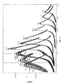
以下、組成比xの違いによる鉛系複合ペロブスカイト化合物の特性の変化をPMN−PTにより説明するが、PZN−PT及びPIN−PTの場合も同様である。図2は、組成比xが互いに異なる厚さ約100μmのPMN−PT(001)板における比誘電率の温度依存性を示すグラフである。比誘電率の測定は、PMN−PT(001)板の両面にそれぞれ設けた電極を通じて10kHz、100kHz又は1MHzの周波数の交流電界をPMN−PT(001)板に印加して行った。印加電界の強度は、測定対象の板の厚みに応じて変えたが、最大で10V/cmとした。 Hereinafter, the change in the characteristics of the lead-based composite perovskite compound due to the difference in the composition ratio x will be described using PMN-PT, but the same applies to PZN-PT and PIN-PT. FIG. 2 is a graph showing the temperature dependence of the relative permittivity of PMN-PT (001) plates having a thickness of about 100 μm and different composition ratios x. The relative dielectric constant was measured by applying an AC electric field having a frequency of 10 kHz, 100 kHz, or 1 MHz to the PMN-PT (001) plate through electrodes provided on both sides of the PMN-PT (001) plate. The intensity of the applied electric field was changed according to the thickness of the plate to be measured, but was 10 V / cm at the maximum.
図2に示すように、印加電界の周波数が高いほど比誘電率は小さい。また図2からは、組成比xが0.1又は0.2のときには比誘電率が比較的大きいことも分かる。誘電率(ε)を真空の誘電率(ε0)で除したものが比誘電率(εr)である(すなわちεr=ε/ε0)ので、誘電率の大きい物質は一般に、比誘電率も大きい。図2で着目すべきは、x=0.1のときには25℃から100℃の間で比誘電率が10000を超えることである。また、x=0.2のときには、100℃においては比誘電率が10000を超えるピークを示すのに対し、50℃において比誘電率が約5000とピークの半分以下であることも着目すべき点である。As shown in FIG. 2, the higher the frequency of the applied electric field, the smaller the relative dielectric constant. FIG. 2 also shows that the relative dielectric constant is relatively large when the composition ratio x is 0.1 or 0.2. The dielectric constant (ε) divided by the vacuum dielectric constant (ε 0 ) is the relative dielectric constant (ε r ) (ie, ε r = ε / ε 0 ). The rate is also great. It should be noted in FIG. 2 that the relative dielectric constant exceeds 10,000 between 25 ° C. and 100 ° C. when x = 0.1. It should also be noted that when x = 0.2, the relative dielectric constant shows a peak exceeding 10,000 at 100 ° C., whereas the relative dielectric constant is about 5000, which is less than half of the peak at 50 ° C. It is.
図3(a)及び図3(b)はPMN−PT固溶体単結晶の状態図を示し、そのうち図3(b)は図3(a)の一部を拡大して示す。図3(a)及び図3(b)において、横軸はPMN−PT中のPbTiO3(PT)の組成比xであり、縦軸は温度である。図3(a)に示すように、PMN−PT固溶体単結晶は、組成比及び温度に応じて、立方晶相、正方晶相、及び疑似立方晶/菱面体晶相のいずれかを示す。図3(a)及び図3(b)においては、正方晶相及び疑似立方晶/菱面体晶相と立方晶相との間の境界を境界線αで示し、疑似立方晶/菱面体晶相と正方晶相との間の境界を境界線MPB(モルフォトロピック相境界)で示す。組成比が一定の場合、ある温度を境に正方晶相又は疑似立方晶/菱面体晶相から立方晶相へ、あるいは立方晶相から正方晶相又は疑似立方晶/菱面体晶相へ結晶相の変化が起こる。この結晶相の変化が起こる温度がキュリー温度である。3 (a) and 3 (b) show phase diagrams of the PMN-PT solid solution single crystal, and FIG. 3 (b) shows a part of FIG. 3 (a) in an enlarged manner. 3A and 3B, the horizontal axis represents the composition ratio x of PbTiO 3 (PT) in PMN-PT, and the vertical axis represents temperature. As shown in FIG. 3A, the PMN-PT solid solution single crystal exhibits any one of a cubic phase, a tetragonal phase, and a pseudo cubic / rhombohedral phase depending on the composition ratio and temperature. 3A and 3B, the boundary between the tetragonal phase and the pseudo cubic / rhombohedral phase and the cubic phase is indicated by a boundary line α, and the pseudo cubic / rhombohedral phase is shown. The boundary between the crystal phase and the tetragonal phase is indicated by the boundary line MPB (morphotropic phase boundary). When the composition ratio is constant, the crystal phase from a tetragonal phase or pseudo cubic / rhombohedral phase to a cubic phase, or from a cubic phase to a tetragonal phase or a pseudo cubic / rhombohedral phase at a certain temperature Changes occur. The temperature at which this crystal phase change occurs is the Curie temperature.
立方晶相のPMN−PT固溶体単結晶は、光遮断性を有する。すなわち、PMN−PT固溶体単結晶の温度がキュリー温度以上のときには組成比xに関わらずPMN−PT固溶体単結晶は光の透過を阻止する。一方、PMN−PT固溶体単結晶の温度がキュリー温度未満の場合には、組成比xが0.2以上であれば、電界が印加されなくても、PMN−PT固溶体単結晶は少なくとも部分的に光の透過を許容する。 The cubic phase PMN-PT solid solution single crystal has light blocking properties. That is, when the temperature of the PMN-PT solid solution single crystal is equal to or higher than the Curie temperature, the PMN-PT solid solution single crystal blocks light transmission regardless of the composition ratio x. On the other hand, when the temperature of the PMN-PT solid solution single crystal is lower than the Curie temperature, if the composition ratio x is 0.2 or more, the PMN-PT solid solution single crystal is at least partially even if no electric field is applied. Allow light transmission.
疑似立方晶/菱面体晶相のPMN−PT固溶体単結晶は、組成比xが0.1よりも大きくかつ0.2よりも小さいときに電界に対してヒステリシスを示す。そして、組成比xが0.1よりも大きくかつ0.2よりも小さいPMN−PT固溶体単結晶は、高誘電率でかつ光の透過を阻止する第1の状態と低誘電率でかつ光の透過を許容する第2の状態との間を変移可能である。また、組成比xが0.1よりも大きくかつ0.2よりも小さいPMN−PT固溶体単結晶はメモリ効果を有する。メモリ効果とは、キュリー温度未満においてPMN−PT固溶体単結晶に対し閾値以上の大きさの電界を一旦印加すると、その後に印加電界の大きさを増加又は減少させたとしてもPMN−PT固溶体単結晶が第2の状態から第1の状態に変移しないことをいう。 The PMN-PT solid solution single crystal having a pseudo cubic / rhombohedral phase exhibits hysteresis with respect to an electric field when the composition ratio x is larger than 0.1 and smaller than 0.2. The PMN-PT solid solution single crystal having a composition ratio x larger than 0.1 and smaller than 0.2 has a high dielectric constant, a first state that blocks light transmission, a low dielectric constant, and light transmission. It is possible to change between the second state that allows transmission. Further, a PMN-PT solid solution single crystal having a composition ratio x larger than 0.1 and smaller than 0.2 has a memory effect. The memory effect means that once an electric field having a magnitude greater than or equal to a threshold value is applied to the PMN-PT solid solution single crystal below the Curie temperature, the PMN-PT solid solution single crystal may be increased or decreased thereafter. Does not change from the second state to the first state.
図3(b)に示すように、組成比xが0.1以下の場合にはキュリー温度は40℃以下と室温又は室温に近くなる。PMN−PT固溶体単結晶は、キュリー温度以上に加熱されると光の透過を阻止する立方晶相に変わる。そのため、キュリー温度が室温又は室温に近い場合には、たとえ閾値以上の大きさの電界を印加することによりPMN−PT固溶体単結晶を低誘電率でかつ光の透過を許容する状態に変移させたとしても、室温又は室温に近い温度で光の透過を許容する第1状態に戻ってしまうため、メモリ効果が妨げられることとなる。よって、より好適にメモリ効果が発揮されるためには、組成比xは0.1よりも大きいことが好ましい。すなわち、より好適にメモリ効果が発揮されるためには、キュリー温度が40℃よりも大きくなるように組成比xを設定することが好ましい。 As shown in FIG. 3B, when the composition ratio x is 0.1 or less, the Curie temperature is 40 ° C. or less, which is room temperature or close to room temperature. When the PMN-PT solid solution single crystal is heated to a temperature equal to or higher than the Curie temperature, the PMN-PT solid solution single crystal changes to a cubic phase that blocks light transmission. Therefore, when the Curie temperature is at or near room temperature, the PMN-PT solid solution single crystal is changed to a state permitting light transmission with a low dielectric constant even by applying an electric field having a magnitude higher than the threshold. However, the memory effect is hindered because the light returns to the first state that allows light transmission at room temperature or a temperature close to room temperature. Therefore, the composition ratio x is preferably larger than 0.1 in order to exhibit the memory effect more suitably. That is, in order to exhibit the memory effect more suitably, it is preferable to set the composition ratio x so that the Curie temperature is higher than 40 ° C.
上記リラクサー強誘電体固溶体単結晶を構成する鉛系複合ペロブスカイト化合物は、疑似立方晶/菱面体晶相(001)板であることが好ましい。疑似立方晶/菱面体晶相(001)板においては、オブリークフィールド(oblique field)と呼ばれるエンジニアドドメイン構造により、電界印加によるドメインウォールの移動を抑制可能である。これにより、リラクサー強誘電体固溶体単結晶は、特異な光特性及び誘電特性を示すだけでなく、疑似立方晶/菱面体晶相(001)板の高い電気機械結合係数及び良好な機械的歪み特性に基づき、良好なアクチュエータ特性も示す。 The lead-based composite perovskite compound constituting the relaxor ferroelectric solid solution single crystal is preferably a pseudo cubic / rhombohedral phase (001) plate. In the pseudo cubic / rhombohedral phase (001) plate, the movement of the domain wall due to the application of an electric field can be suppressed by an engineered domain structure called an oblique field. As a result, the relaxor ferroelectric solid solution single crystal not only exhibits unique optical and dielectric properties, but also has a high electromechanical coupling coefficient and good mechanical strain characteristics of the pseudo cubic / rhombohedral phase (001) plate. Based on the above, good actuator characteristics are also shown.
本発明の別の態様では、上記リラクサー強誘電体固溶体単結晶を用いたデバイスが提供される。該デバイスにおいては、リラクサー強誘電体固溶体単結晶の少なくとも光特性が利用されることが好ましく、光特性の変化に伴って現れるリラクサー強誘電体固溶体単結晶の誘電特性の変化が光特性とともに利用されてもよい。 In another aspect of the present invention, a device using the relaxor ferroelectric solid solution single crystal is provided. In the device, it is preferable that at least the optical properties of the relaxor ferroelectric solid solution single crystal are used, and the change in the dielectric properties of the relaxor ferroelectric solid solution single crystal that appears along with the change in the optical properties is used together with the optical properties. May be.
本発明のさらに別の態様では、上記リラクサー強誘電体固溶体単結晶を含むデバイスの使用方法が提供される。該方法は、デバイス中のリラクサー強誘電体固溶体単結晶を第1の状態から第2の状態に変移させるべく、リラクサー強誘電体固溶体単結晶に閾値以上の大きさの電界を印加する工程と、デバイス中のリラクサー強誘電体固溶体単結晶を第2の状態から第1の状態に変移させるべく、リラクサー強誘電体固溶体単結晶をキュリー温度以上に加熱する工程とを備える。 In still another aspect of the present invention, a method of using a device including the relaxor ferroelectric solid solution single crystal is provided. The method includes applying an electric field having a magnitude equal to or greater than a threshold value to the relaxor ferroelectric solid solution single crystal to shift the relaxor ferroelectric solid solution single crystal in the device from the first state to the second state; Heating the relaxor ferroelectric solid solution single crystal to a temperature equal to or higher than the Curie temperature in order to change the relaxor ferroelectric solid solution single crystal in the device from the second state to the first state.
以下、本発明の一実施形態を説明する。 Hereinafter, an embodiment of the present invention will be described.
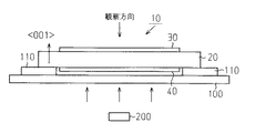
図1に示す本実施形態に係る光デバイス10は、デバイス本体20と、一対の透明電極30,40を備える。デバイス本体20は、PMN−PT(001)板から薄板状に形成されている。PMN−PT(001)板の(001)は、結晶面の指数を表す。透明電極30,40は、デバイス本体20の上面及び下面の上にそれぞれ設けられている。透明電極30,40は金からなり、スパッタリングや蒸着等の物理的成膜法にて形成されている。
The
上記光デバイス10の光特性の観察は、偏光顕微鏡による観察を通じて行なった。より具体的には、図1に示すように、一対のガラス台110を上面に有する透明ガラス板100を用意し、両ガラス台110にまたがるようにして光デバイス10をガラス板100上に載置した。そして、透明ガラス板100の下方から光デバイス10に向かって光源200からの偏光を投射しながら、直交ニコル下で偏光顕微鏡により光デバイス10を観察した。なお、図1中の<001>は晶帯軸の指数である。
The optical characteristics of the
透明電極30,40は図示しないリード線及び可変抵抗を介して図示しない直流電源に接続されており、両透明電極30,40間には異なる値の電圧を印加可能である。前記リード線には図示しない切換回路が設けられている。切換回路の切り換えによって両透明電極30,40間には正極性又は逆極性の電圧を印加可能である。また、両透明電極30,40は、デバイス本体20(PMN−PT)の誘電率を測定するための電極としても機能し、光デバイス10がPMN−PTの光特性だけを利用するデバイスとしてではなく、光特性の変化に伴って現れるPMN−PTの誘電特性の変化も光特性とともに利用するデバイスとして電子回路的に使用される際には、コンデンサ出力端子としても利用される。
The
以下、本発明の実施例及び比較例について説明する。なお、以下の観察及び測定は、特に断らない限り、いずれも室温(25℃)で行った。 Examples of the present invention and comparative examples will be described below. The following observations and measurements were performed at room temperature (25 ° C.) unless otherwise specified.
PMN−PT(001)板から形成した厚さ122μmのデバイス本体を用いて実施例1,2及び比較例1〜4の光デバイスを作成した。ただし、PMN−PT中のPbTiO3の組成比xは、実施例1においては0.15、実施例2においては0.13、比較例1においては0.2、比較例2においては0.28、比較例3においては0.1、比較例4においては0.06である。Optical devices of Examples 1 and 2 and Comparative Examples 1 to 4 were prepared using a device body having a thickness of 122 μm formed from a PMN-PT (001) plate. However, the composition ratio x of PbTiO 3 in PMN-PT is 0.15 in Example 1, 0.13 in Example 2, 0.2 in Comparative Example 1, and 0.28 in Comparative Example 2. In Comparative Example 3, it is 0.1, and in Comparative Example 4, it is 0.06.
図8は、0kV/cmから8.2kV/cmにまで一方向に変化した後に8.2kV/cmから−8.2kV/cmにまで一方向に変化する電界を実施例1の光デバイスに印加しながらデバイス本体(PMN−PT)の比誘電率を測定した結果を示す。なお、電界の印加を開始する前のデバイス本体中のPMN−PTは、高誘電率でかつ光の透過を阻止する状態であった。 FIG. 8 shows that an electric field that changes in one direction from 8.2 kV / cm to −8.2 kV / cm after changing in one direction from 0 kV / cm to 8.2 kV / cm is applied to the optical device of Example 1. The result of measuring the relative dielectric constant of the device body (PMN-PT) is shown. Note that the PMN-PT in the device body before the application of the electric field was in a state of high dielectric constant and blocking light transmission.
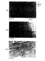
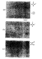
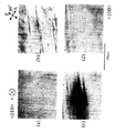
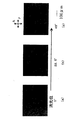
図4(a)〜(c)は、電界が印加されていない状態の実施例1及び比較例1,2の光デバイスのデバイス本体を直交ニコル下で偏光顕微鏡を用いて観察した結果を示す。図4(a)は、実施例1の光デバイス10における観察結果であり、全体にわたって光の透過が阻止されている様子を示している。図4(b)は、比較例1の光デバイスにおける観察結果であり、部分的に光の透過が許容されている様子を示している。図4(c)は、比較例2の光デバイスにおける観察結果であり、全体にわたって光の透過が許容されている様子を示している。
4A to 4C show the results of observing the device bodies of the optical devices of Example 1 and Comparative Examples 1 and 2 in a state where no electric field is applied, using a polarizing microscope under crossed Nicols. FIG. 4A is an observation result in the
図11(a)〜(c)は、図4(a)と同様、電界が印加されていない状態の実施例1の光デバイスのデバイス本体を直交ニコル下で偏光顕微鏡を用いて観察した結果を示す。ただし、図11(a)は、ステイジの回転角度が0°のときの観察結果であり、図11(b)は、回転角度が22.5°のときの観察結果であり、図11(c)は、回転角度が45°のときの観察結果である。図11(a)〜(c)に示すように、いずれの回転角度においても消光位又は対角位を示すことなく暗視野像が観察されており、この結果から、電界が印加されていない状態の実施例1の光デバイスでは、PMN−PTが光の透過を阻止する状態にあることが分かる。 11 (a) to 11 (c) show the results of observing the device body of the optical device of Example 1 in the state where no electric field is applied using a polarizing microscope under crossed Nicols, as in FIG. 4 (a). Show. However, FIG. 11A shows the observation result when the rotation angle of the stage is 0 °, and FIG. 11B shows the observation result when the rotation angle is 22.5 °, and FIG. ) Is an observation result when the rotation angle is 45 °. As shown in FIGS. 11A to 11C, a dark field image is observed without showing a quenching position or a diagonal position at any rotation angle. From this result, a state in which no electric field is applied is observed. In the optical device of Example 1, it can be seen that PMN-PT is in a state of blocking light transmission.
図11(a)〜(c)に示す結果からは、電界が印加されていない状態の実施例1の光デバイスではPMN−PTのドメイン配列が無秩序であるか或いはドメインサイズが小さく、そのために光の透過が許容されないことが考えられる。電界が印加されていない状態の実施例1の光デバイスでは、図8に示すように、PMN−PTの比誘電率は9500前後(9000〜10000)と高い値を示す。またこのときのPMN−PTの比誘電率及び誘電正接の温度依存性は、図12(a),(b)に示すように、リラクサー特有のVogel-Fulcherタイプの誘電分散を示す。比誘電率及び誘電正接の温度依存性は、直流電源ではなく交流電源を用いてPMN−PTに電界を印加しながらLCRメータにより測定した。印加電界の強度は10V/cmであり、周波数は1kHZ、10kHz、100kHz又は1MHzである。 From the results shown in FIGS. 11 (a) to 11 (c), in the optical device of Example 1 in the state where no electric field is applied, the domain arrangement of PMN-PT is disordered or the domain size is small. It is conceivable that the transmission of is not allowed. In the optical device of Example 1 in a state where no electric field is applied, the relative dielectric constant of PMN-PT shows a high value of around 9500 (9000 to 10000) as shown in FIG. Further, the temperature dependence of the relative dielectric constant and dielectric loss tangent of PMN-PT at this time shows Vogel-Fulcher type dielectric dispersion peculiar to the relaxer, as shown in FIGS. The temperature dependence of the dielectric constant and dielectric loss tangent was measured with an LCR meter while applying an electric field to the PMN-PT using an AC power supply instead of a DC power supply. The intensity of the applied electric field is 10 V / cm, and the frequency is 1 kHz, 10 kHz, 100 kHz, or 1 MHz.
上述及び後述の偏光顕微鏡での観察においては、540nmを中心に400〜600nmの波長範囲を有するハロゲン光源が用いられる。偏光顕微鏡による観察結果を示す図面において、Aは検光子、Pは偏光子を示す。また、電界を印加しながら偏光顕微鏡により観察した結果を示す図面には電界の印加方向を表す記号も併せて示す。直交ニコル下では、検光子Aと偏光子Pは、互いの間に試料を置いた状態で、互いに直交させて用いられる。もし試料が光学的に等方であれば偏光顕微鏡による観察結果は暗視野となり、光学的に異方であれば観察結果は明視野となる。強誘電体の試料は一般に異方体であるが、偏光子Pを分極方向に合わせると観察結果は暗視野になる。この現象は消光と呼ばれる。実施例1の光デバイスのPMN−PTの結晶相は室温(25℃)では菱面体晶相であり、菱面体晶相のPMN−PT(001)板の分極方向は<110>方向に一致する。従って、x軸から45°傾いた位置では暗視野となり、x軸から60°又は30°傾いた位置では明視野となる。最も明るくなる位置は対角位と呼ばれ、菱面体晶相(001)板では対角位はx軸又はy軸に現れる。 In the observation with the polarizing microscope described above and later, a halogen light source having a wavelength range of 400 to 600 nm centering on 540 nm is used. In the drawings showing the observation results with a polarizing microscope, A represents an analyzer and P represents a polarizer. The drawing showing the result of observation with a polarizing microscope while applying an electric field also shows a symbol indicating the direction of application of the electric field. Under crossed Nicols, the analyzer A and the polarizer P are used so as to be orthogonal to each other with a sample placed between them. If the sample is optically isotropic, the observation result by the polarizing microscope is a dark field, and if the sample is optically anisotropic, the observation result is a bright field. Ferroelectric samples are generally anisotropic, but when the polarizer P is aligned with the polarization direction, the observation result becomes a dark field. This phenomenon is called quenching. The crystal phase of PMN-PT of the optical device of Example 1 is a rhombohedral phase at room temperature (25 ° C.), and the polarization direction of the rhombohedral phase PMN-PT (001) plate coincides with the <110> direction. . Accordingly, a dark field is obtained at a position inclined 45 ° from the x axis, and a bright field is obtained at a position inclined 60 ° or 30 ° from the x axis. The brightest position is called the diagonal position. In the rhombohedral phase (001) plate, the diagonal position appears on the x-axis or y-axis.
なお、後述の図9及び図10に示す観察結果を得るときには、正方晶相のPMN−PTの観察に適するように、検光子A及び偏光子Pが基準位置から60°傾いて配置される。正方晶相のPMN−PT(001)板においては、消光位がx軸又はy軸に現れ、x軸とy軸の中間位置で明視野像が観察される。PMN−PT中のPbTiO3の組成比がある程度高いときには、図3(a)に示すように、PMN−PTの結晶相は常温において菱面体晶相ではなく正方晶相である。又、非常に強い電界を印加したときには、PMN−PTの結晶相が菱面体晶相から正方晶相に変化する。When obtaining the observation results shown in FIGS. 9 and 10 to be described later, the analyzer A and the polarizer P are inclined by 60 ° from the reference position so as to be suitable for observing the tetragonal PMN-PT. In a tetragonal PMN-PT (001) plate, the extinction position appears on the x-axis or the y-axis, and a bright-field image is observed at an intermediate position between the x-axis and the y-axis. When the composition ratio of PbTiO 3 in PMN-PT is high to some extent, as shown in FIG. 3A, the crystal phase of PMN-PT is not a rhombohedral phase but a tetragonal phase at room temperature. Further, when a very strong electric field is applied, the crystal phase of PMN-PT changes from a rhombohedral phase to a tetragonal phase.
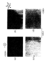
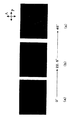
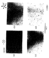
図5(a)〜(c)は、比較例3の光デバイスのデバイス本体を直交ニコル下で偏光顕微鏡を用いて観察した結果を示す。図5(a)は、電界が印加されていない状態における観察結果であり、全体にわたって光の透過が阻止されている様子を示している。図5(b)は、23kV/cmの電界が印加された状態における対角位での観察結果であり、明視野像が観察された。図5(c)は、23kV/cmの電界が印加された状態における消光位での観察結果であり、暗視野像が観察された。 5A to 5C show the results of observing the device body of the optical device of Comparative Example 3 using a polarizing microscope under crossed Nicols. FIG. 5A shows an observation result in a state where no electric field is applied, and shows a state where light transmission is blocked throughout. FIG. 5B is an observation result at a diagonal position in a state where an electric field of 23 kV / cm was applied, and a bright-field image was observed. FIG. 5C shows an observation result at an extinction position in a state where an electric field of 23 kV / cm was applied, and a dark field image was observed.
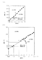
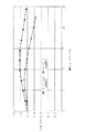
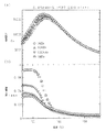
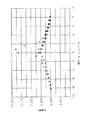
図6は、比較例3,4の光デバイスにおける後述する誘電率の変化の電界依存性を示すグラフである。誘電率の変化はε(E)/ε(0)で表され、ε(E)をε(0)で除することにより求められる。ε(0)は、室温(25℃)下で周波数1MHz及び強度10V/cmの交流電界を印加した状態において測定されるPMN−PTの誘電率である。ε(E)は、室温(25℃)下で直流電界Eを印加した状態に置いて測定されるPMN−PTの誘電率である。図6において、横軸は、PMN−PTに印加される直流電界Eの強度を示し、縦軸はε(E)/ε(0)を示す。図6に示すように、比較例3,4ともε(E)/ε(0)は印加電界の強度に応じて比較的なだらかに変化する。FIG. 6 is a graph showing the electric field dependence of a change in dielectric constant described later in the optical devices of Comparative Examples 3 and 4. The change in dielectric constant is expressed by ε (E) / ε (0) , and is obtained by dividing ε (E) by ε (0) . ε (0) is a dielectric constant of PMN-PT measured in a state where an AC electric field having a frequency of 1 MHz and an intensity of 10 V / cm is applied at room temperature (25 ° C.). ε (E) is a dielectric constant of PMN-PT measured by applying a DC electric field E at room temperature (25 ° C.). In FIG. 6, the horizontal axis indicates the intensity of the DC electric field E applied to PMN-PT, and the vertical axis indicates ε (E) / ε (0) . As shown in FIG. 6, in Comparative Examples 3 and 4, ε (E) / ε (0) changes relatively gently according to the strength of the applied electric field.
図5(a)〜(c)及び図6に示す結果から、比較例3の光デバイスのPMN−PTは、電界が印加されていない状態では光の透過を阻止するが、23kV/cmの電界が印加された状態では光の透過を許容することが分かる。しかしながら、比較例3,4の光デバイスのPMN−PTはともに電界に対するヒステリシスを示さない。 From the results shown in FIGS. 5A to 5C and FIG. 6, the PMN-PT of the optical device of Comparative Example 3 blocks the transmission of light when no electric field is applied, but the electric field of 23 kV / cm. It can be seen that light transmission is allowed in a state where is applied. However, the PMN-PTs of the optical devices of Comparative Examples 3 and 4 do not exhibit hysteresis with respect to the electric field.
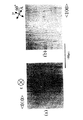
図7(a)〜(d)は、0kV/cmから8.2kV/cmにまで一方向に変化する電界を実施例1の光デバイスに印加しながらデバイス本体を直交ニコル下で偏光顕微鏡を用いて観察した結果を示す。図7(a)は、電界が印加されていない状態における観察結果である。図7(b)は、1.6kV/cmの電界が印加された状態における観察結果である。図7(c)は、4.9kV/cmの電界が印加された状態における観察結果である。図7(d)は、8.2kV/cmの電界が印加された状態における観察結果である。 7 (a) to 7 (d), using a polarization microscope under crossed Nicols while applying an electric field that changes in one direction from 0 kV / cm to 8.2 kV / cm to the optical device of Example 1. The observation results are shown. FIG. 7A shows an observation result in a state where no electric field is applied. FIG. 7B shows an observation result in a state where an electric field of 1.6 kV / cm is applied. FIG. 7C shows an observation result in a state where an electric field of 4.9 kV / cm is applied. FIG. 7D shows an observation result in a state where an electric field of 8.2 kV / cm is applied.
閾値(実施例1では2kV/cm)以上の大きさの電界が印加されると、図7(c),(d)に示すように、デバイス本体中のPMN−PTは光の透過を阻止する状態から光の透過を許容する状態に変移する。それと同時に、図8に示すように、PMN−PTの比誘電率は6000前後(5000〜7000)にまでおよそ半減する。印加電界がさらに正に大きくなっても、光の透過が許容され続けると同時に、比誘電率は漸減しながら低く保たれる。 When an electric field having a threshold value (2 kV / cm in the first embodiment) or higher is applied, the PMN-PT in the device body blocks light transmission as shown in FIGS. Transition from a state to a state allowing light transmission. At the same time, as shown in FIG. 8, the relative dielectric constant of PMN-PT is approximately halved to around 6000 (5000 to 7000). Even if the applied electric field further increases positively, light transmission continues to be allowed, and at the same time, the relative dielectric constant is kept low while gradually decreasing.
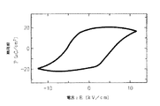
図13は、実施例1の光デバイスのPMN−PTにおける分極−電界履歴曲線を示す。分極−電界履歴曲線は公知のソーヤータワー回路を用いて周波数50Hzの交流電界のもとで測定した。図13から分かるように、低誘電率でかつ光の透過を許容する状態はメモリ効果により記憶される。すなわち、印加電界の大きさを増加又は減少させたとしても、低誘電率でかつ光の透過を許容する状態は維持される。 FIG. 13 shows a polarization-electric field history curve in PMN-PT of the optical device of Example 1. The polarization-electric field history curve was measured under a 50 Hz frequency alternating electric field using a known saw tower circuit. As can be seen from FIG. 13, the low dielectric constant and the state allowing light transmission are stored by the memory effect. That is, even if the magnitude of the applied electric field is increased or decreased, a state where the permittivity of light is allowed to pass with a low dielectric constant is maintained.
図9(a),(b)は、8.2kV/cmから0kV/cmにまで一方向に変化する電界を実施例1の光デバイスに印加しながらデバイス本体を直交ニコル下で偏光顕微鏡を用いて観察した結果を示す。図9(a)は、8.2kV/cmの電界が印加された状態における観察結果である。図9(b)は、電界が印加されていない状態における観察結果である。このように8.2kV/cmから0kV/cmにまで一方向に変化する電界を印加した場合には、図8に示すように、誘電率が低く保たれると同時に、図9(a),(b)に示すように光の透過も許容され続ける。 9 (a) and 9 (b) show that a device body is used with a polarizing microscope under crossed Nicols while applying an electric field changing in one direction from 8.2 kV / cm to 0 kV / cm to the optical device of Example 1. The observation results are shown. FIG. 9A shows an observation result in a state where an electric field of 8.2 kV / cm is applied. FIG. 9B shows an observation result in a state where no electric field is applied. When an electric field that changes in one direction from 8.2 kV / cm to 0 kV / cm is applied in this way, the dielectric constant is kept low as shown in FIG. Transmission of light continues to be allowed as shown in (b).
図10(a)〜(d)は、0kV/cmから−8.2kV/cmにまで一方向に変化する電界を実施例1の光デバイスに印加しながらデバイス本体を直交ニコル下で偏光顕微鏡を用いて観察した結果を示す。図10(a)は、電界が印加されていない状態における観察結果である。図10(b)は、−0.8kV/cmの電界が印加された状態における観察結果である。図10(c)は、−4.9kV/cmの電界が印加された状態における観察結果である。図10(d)は、−8.2kV/cmの電界が印加された状態における観察結果である。 FIGS. 10A to 10D show a polarization microscope under crossed Nicols while applying an electric field that changes in one direction from 0 kV / cm to −8.2 kV / cm to the optical device of Example 1. The result observed using this is shown. FIG. 10A shows an observation result in a state where no electric field is applied. FIG. 10B shows an observation result in a state where an electric field of −0.8 kV / cm is applied. FIG. 10C shows an observation result in a state where an electric field of −4.9 kV / cm is applied. FIG. 10D shows an observation result in a state where an electric field of −8.2 kV / cm is applied.
このように0kV/cmから−8.2kV/cmにまで一方向に変化する電界を印加した場合には、電界が所定の誘電異常閾値(実施例1では−0.8kV/cm)を超えるときに誘電異常が発生して分極反転が起こる。それに伴い、PMN−PTのドメイン構造には変化が生じる。電界が−0.8kV/cmのときの誘電異常は、図8のグラフで観察可能である。印加電界がさらに負に大きくなっても、光の透過が許容され続けると同時に、誘電率は漸減しながら低く保たれる。 When an electric field that changes in one direction from 0 kV / cm to -8.2 kV / cm is applied in this way, the electric field exceeds a predetermined dielectric anomaly threshold (-0.8 kV / cm in Example 1). Dielectric anomalies occur and polarization reversal occurs. Along with this, changes occur in the domain structure of PMN-PT. The dielectric anomaly when the electric field is -0.8 kV / cm can be observed in the graph of FIG. Even if the applied electric field is further increased negatively, the transmission of light continues to be allowed and at the same time the dielectric constant is kept low while decreasing.
上記したように、印加電界の大きさを増加又は減少させたとしても、低誘電率でかつ光の透過を許容する状態は維持される。低誘電率でかつ光の透過を許容する状態から高誘電率でかつ光の透過を阻止する最初の状態にPMN−PTが変移するためには、デバイス本体をキュリー温度以上に加熱することが必要である。 As described above, even when the magnitude of the applied electric field is increased or decreased, the state of permitting light transmission with a low dielectric constant is maintained. In order for PMN-PT to transition from a low dielectric constant and allowing light transmission to a high dielectric constant and preventing light transmission, it is necessary to heat the device body above the Curie temperature. It is.
図14(a)〜(c)は、キュリー温度以上にまで加熱した後の印加電界がゼロのときの実施例1の光デバイスのデバイス本体を直交ニコル下で偏光顕微鏡を用いて観察した結果を示す。図14(a)は消光位での観察結果であり、図14(b)はステイジの回転角度が22.5°のときの観察結果であり、図14(c)は回転角度が45°のときの観察結果である。図14(a)〜(c)に示すように、いずれの回転角度においても暗視野像が観察されており、この結果から、キュリー温度以上にまで加熱した後のPMN−PTが光の透過を阻止する状態にあることが分かる。 14 (a) to 14 (c) show the results of observing the device body of the optical device of Example 1 with a polarizing microscope under crossed Nicols when the applied electric field after heating to the Curie temperature or higher is zero. Show. 14A shows the observation result at the extinction position, FIG. 14B shows the observation result when the rotation angle of the stage is 22.5 °, and FIG. 14C shows the rotation angle of 45 °. It is an observation result. As shown in FIGS. 14A to 14C, a dark field image is observed at any rotation angle. From this result, PMN-PT after heating up to the Curie temperature or higher does not transmit light. It turns out that it is in the state to stop.
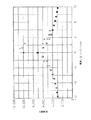
図15は、キュリー温度以上にまで加熱した後の実施例1の光デバイスにおける比誘電率の電界依存性を示すグラフである。図15において、△は、ゼロを始点に正方向に電界を変化させながら計測される点を示す。□は、引き続き正から負に向かって電界を一方向に変化させながら計測される点を示す。×は、引き続き負から正に向かって電界を一方向に変化させながら計測される点を示す。○は、さらに引き続き正からゼロに向かって電界を一方向に変化させながら計測される点を示す。図15に示すように、キュリー温度以上にまで加熱された後のPMN−PTの比誘電率は10000前後(9000〜12000)と高い値を示す。しかし、閾値以上の大きさの電界が印加されると比誘電率は大きく減少し、5000前後(4000〜7000)にまでおよそ半減する。また、閾値以上の大きさの電界が一旦印加された後は、正から負又は負から正にいくら電界を変化させたとしても、比誘電率は低いまま維持される。 FIG. 15 is a graph showing the electric field dependence of the relative permittivity of the optical device of Example 1 after being heated to the Curie temperature or higher. In FIG. 15, Δ indicates a point measured while changing the electric field in the positive direction starting from zero. A square indicates a point measured while changing the electric field in one direction from positive to negative. X indicates a point measured while changing the electric field in one direction from negative to positive. A circle indicates a point that is further measured while changing the electric field in one direction from positive to zero. As shown in FIG. 15, the relative dielectric constant of PMN-PT after being heated to the Curie temperature or higher shows a high value of around 10,000 (9000 to 12000). However, when an electric field larger than the threshold value is applied, the relative dielectric constant is greatly reduced, and is approximately halved to around 5000 (4000 to 7000). In addition, once an electric field having a magnitude equal to or greater than the threshold is applied, the relative permittivity is kept low even if the electric field is changed from positive to negative or from negative to positive.
図16は、実施例2の光デバイスにおける比誘電率の電界依存性を示すグラフである。図16において、△は、ゼロを始点に正方向に電界を変化させながら計測される点を示す。□は、引き続き正から負に向かって電界を一方向に変化させながら計測される点を示す。×は、引き続き負から正に向かって電界を一方向に変化させながら計測される点を示す。○は、さらに引き続き正からゼロに向かって電界を一方向に変化させながら計測される点を示す。図16に示すように、キュリー温度以上にまで加熱された後のPMN−PTの比誘電率は10000前後(9000〜12000)と高い値を示す。しかし、閾値以上の大きさの電界が印加されると比誘電率は大きく減少し、5000前後(3000〜7000)にまでおよそ半減する。実施例2の光デバイスにおいても、実施例1の光デバイスと同様、閾値以上の大きさの電界が一旦印加された後は、正から負又は負から正にいくら電界を変化させたとしても、誘電率は低いまま維持される。 FIG. 16 is a graph showing the electric field dependence of the dielectric constant in the optical device of Example 2. In FIG. 16, Δ indicates a point measured while changing the electric field in the positive direction starting from zero. A square indicates a point measured while changing the electric field in one direction from positive to negative. X indicates a point measured while changing the electric field in one direction from negative to positive. A circle indicates a point that is further measured while changing the electric field in one direction from positive to zero. As shown in FIG. 16, the relative dielectric constant of PMN-PT after being heated to the Curie temperature or higher shows a high value of around 10,000 (9000 to 12000). However, when an electric field larger than the threshold value is applied, the relative permittivity is greatly reduced, and is approximately halved to around 5000 (3000 to 7000). Even in the optical device of the second embodiment, as with the optical device of the first embodiment, once an electric field having a magnitude equal to or greater than the threshold is applied, no matter how much the electric field is changed from positive to negative or from negative to positive, The dielectric constant remains low.
電界が印加されていない状態の実施例2の光デバイスのデバイス本体を直交ニコル下で偏光顕微鏡を用いて観察した。図示はしないが、電界が印加されていない状態の実施例2の光デバイスでは、PMN−PTが光の透過を阻止する状態であることが確認された。 The device body of the optical device of Example 2 in a state where no electric field was applied was observed using a polarizing microscope under crossed Nicols. Although not shown, it was confirmed that in the optical device of Example 2 in which no electric field was applied, PMN-PT was in a state of blocking light transmission.
図17(a)〜(d)は、0kV/cmから11.7kV/cmにまで一方向に変化した後に11.7kV/cmから0kV/cmにまで一方向に変化する電界を実施例2の光デバイスに印加しながらデバイス本体を直交ニコル下で偏光顕微鏡を用いて観察した結果を示す。図17(a)は、電界が印加されていない状態における観察結果である。図17(b)は、7.0kV/cmの電界が印加された状態における観察結果である。図17(c)は、11.7kV/cmの電界が印加された状態における観察結果である。図17(d)は、11.7kV/cmの電界が一旦印加された後の電界が印加されていない状態における観察結果である。 17 (a) to 17 (d) show an electric field that changes in one direction from 11.7 kV / cm to 0 kV / cm after changing in one direction from 0 kV / cm to 11.7 kV / cm. The result of having observed the device main body using the polarization microscope under crossed Nicols, applying to an optical device is shown. FIG. 17A shows an observation result in a state where no electric field is applied. FIG. 17B shows an observation result in a state where an electric field of 7.0 kV / cm is applied. FIG. 17C shows an observation result in a state where an electric field of 11.7 kV / cm is applied. FIG. 17D shows an observation result in a state where an electric field of 11.7 kV / cm is once applied and no electric field is applied.
閾値(実施例2では3kV/cm)以上の大きさの電界が印加されると、図17(b)〜(d)に示すように、デバイス本体中のPMN−PTは光の透過を阻止する状態から光の透過を許容する状態に変移する。それと同時にPMN−PTは、図16に示すように、低い比誘電率(誘電率)を示す。印加電界がさらに正に大きくなっても、光の透過が許容され続けると同時に、誘電率は漸減しながら低く保たれる。 When an electric field having a threshold value (3 kV / cm in Example 2) or more is applied, PMN-PT in the device body blocks light transmission, as shown in FIGS. Transition from a state to a state allowing light transmission. At the same time, PMN-PT exhibits a low relative dielectric constant (dielectric constant) as shown in FIG. Even if the applied electric field is further increased positively, the transmission of light continues to be allowed and at the same time the dielectric constant is kept low while decreasing.
11.7kV/cmから0kV/cmにまで一方向に変化する電界を実施例2の光デバイスに印加した場合には、図16に示すように、比誘電率がおよそ7000と低く保たれる。それと同時に、図17(d)に示すように、光の透過も許容され続ける。 When an electric field that changes in one direction from 11.7 kV / cm to 0 kV / cm is applied to the optical device of Example 2, the relative dielectric constant is kept as low as about 7000, as shown in FIG. At the same time, as shown in FIG. 17D, transmission of light continues to be allowed.
高誘電率でかつ光の透過を阻止する状態から低誘電率でかつ光の透過を許容する状態へとPMN−PTが変移する閾値は、実施例1では2kV/cm、実施例2では3kV/cmと異なる。一般に、PMN−PT中のPbTiO3の組成比が小さくなるにつれて閾値は大きくなる。The threshold at which PMN-PT shifts from a state having a high dielectric constant and blocking light transmission to a state having a low dielectric constant and allowing light transmission is 2 kV / cm in Example 1 and 3 kV / cm in Example 2. Different from cm. Generally, the threshold value increases as the composition ratio of PbTiO 3 in PMN-PT decreases.
前記実施形態を次のように変更してもよい。 You may change the said embodiment as follows.
光デバイス10を光メモリとして具体化してもよい。この場合、光メモリは、光の透過を許容する状態と光の透過を阻止する状態の二進信号として情報を記憶する。デバイス本体20は光の透過を許容する状態のときには低誘電率を示し、光の透過を阻止する状態のときには高誘電率を示す。従って、誘電率の違いを電圧の変化として検出することにより、記憶した内容を簡単に読み出すことができる。
The
従来、光を使用して情報を記憶させる技術としては、光磁気ディスクがある。光磁気ディスクでは、媒体の特定部分にレーザ光を照射することにより、照射された特定部分をキュリー温度以上に加熱し、該特定部分の保持力が弱くなったところで、外部磁界を付与することにより、上向き或いは下向きに磁化させ、磁化した部分に情報を二進信号として記憶する。このように、光磁気ディスクの場合は、特定部分にレーザ光を照射してキュリー温度以上に上昇させたうえで、磁界を上向き又は下向きに区別して印加させる必要がある。それに対して、光デバイス10を光メモリとして具体化した場合には、キュリー温度以上に加熱するか否かによって、特定部分を光の透過を許容する状態(オン)及び光の透過を阻止する状態(オフ)のいずれかにすることができる。
Conventionally, there is a magneto-optical disk as a technique for storing information using light. In a magneto-optical disk, by irradiating a specific portion of the medium with laser light, the irradiated specific portion is heated to a temperature above the Curie temperature, and when the holding force of the specific portion becomes weak, an external magnetic field is applied. The magnetized portion is magnetized upward or downward, and information is stored as a binary signal in the magnetized portion. As described above, in the case of a magneto-optical disk, it is necessary to irradiate a specific portion with a laser beam and raise the temperature to the Curie temperature or higher, and then apply a magnetic field by distinguishing the magnetic field upward or downward. On the other hand, when the
光デバイス10を光バルブとして具体化してもよい。この場合、光バルブは、光の透過を許容する状態と光の透過を阻止する状態との間を切り替わることによって、光の出入りを調節する。デバイス本体20は光の透過を許容する状態のときには低誘電率を示し、光の透過を阻止する状態のときには高誘電率を示す。従って、誘電率の違いを電圧の変化として検出することにより、光バルブの動作を検出することが可能である。
The
光デバイス10のデバイス本体20は、PMN−PTの代わりに、PZN−PT又はPIN−PTから形成されてもよい。
The
光デバイス10は、PMN−PTの光特性及び誘電特性に加えてPMN−PTの圧電特性も利用したアクチュエータとして利用されてもよい。
The
上記リラクサー強誘電体固溶体単結晶は、(1−x)Pb(Mg1/3Nb2/3)O3・xPbTiO 3 で表される化合物であってもよい。上記組成式中のxは、(1−x)Pb(Mg 1/3 Nb 2/3 )O 3 ・xPbTiO 3 中のPbTiO3の組成比を示す。以下の説明においては、(1−x)Pb(Mg1/3Nb2/3)O3・xPbTiO3をPMN−PTと略称する。PMN−PTは、組成比xが0.1よりも大きくかつ0.2よりも小さい範囲において、電界印加により第1の状態と第2の状態の間を変移可能である。
Said relaxor ferroelectric solid solution single crystal may be a compound represented by (1-x) Pb (Mg 1/3
以下、組成比xの違いによるPMN−PTの特性の変化を説明する。図2は、組成比xが互いに異なる厚さ約100μmのPMN−PT(001)板における比誘電率の温度依存性を示すグラフである。比誘電率の測定は、PMN−PT(001)板の両面にそれぞれ設けた電極を通じて10kHz、100kHz又は1MHzの周波数の交流電界をPMN−PT(001)板に印加して行った。印加電界の強度は、測定対象の板の厚みに応じて変えたが、最大で10V/cmとした。 Hereinafter, Ru theory Aquiraz a change in characteristics of the PMN-PT due to a difference in composition ratio x. FIG. 2 is a graph showing the temperature dependence of the relative permittivity of PMN-PT (001) plates having a thickness of about 100 μm and different composition ratios x. The relative dielectric constant was measured by applying an AC electric field having a frequency of 10 kHz, 100 kHz, or 1 MHz to the PMN-PT (001) plate through electrodes provided on both sides of the PMN-PT (001) plate. The intensity of the applied electric field was changed according to the thickness of the plate to be measured, but was 10 V / cm at the maximum.
図3(b)に示すように、組成比xが0.1以下の場合にはキュリー温度は40℃以下と室温又は室温に近くなる。PMN−PT固溶体単結晶は、キュリー温度以上に加熱されると光の透過を阻止する立方晶相に変わる。そのため、キュリー温度が室温又は室温に近い場合には、たとえ閾値以上の大きさの電界を印加することによりPMN−PT固溶体単結晶を低誘電率でかつ光の透過を許容する状態に変移させたとしても、室温又は室温に近い温度で光の透過を阻止する第1状態に戻ってしまうため、メモリ効果が妨げられることとなる。よって、より好適にメモリ効果が発揮されるためには、組成比xは0.1よりも大きいことが好ましい。すなわち、より好適にメモリ効果が発揮されるためには、キュリー温度が40℃よりも大きくなるように組成比xを設定することが好ましい。 As shown in FIG. 3B, when the composition ratio x is 0.1 or less, the Curie temperature is 40 ° C. or less, which is room temperature or close to room temperature. When the PMN-PT solid solution single crystal is heated to a temperature equal to or higher than the Curie temperature, the PMN-PT solid solution single crystal changes to a cubic phase that blocks light transmission. Therefore, when the Curie temperature is at or near room temperature, the PMN-PT solid solution single crystal is changed to a state permitting light transmission with a low dielectric constant even by applying an electric field having a magnitude higher than the threshold. However, the memory effect is hindered because the light returns to the first state in which light transmission is blocked at room temperature or a temperature close to room temperature. Therefore, the composition ratio x is preferably larger than 0.1 in order to exhibit the memory effect more suitably. That is, in order to exhibit the memory effect more suitably, it is preferable to set the composition ratio x so that the Curie temperature is higher than 40 ° C.
従来、光を使用して情報を記憶させる技術としては、光磁気ディスクがある。光磁気ディスクでは、媒体の特定部分にレーザ光を照射することにより、照射された特定部分をキュリー温度以上に加熱し、該特定部分の保磁力が弱くなったところで、外部磁界を付与することにより、上向き或いは下向きに磁化させ、磁化した部分に情報を二進信号として記憶する。このように、光磁気ディスクの場合は、特定部分にレーザ光を照射してキュリー温度以上に上昇させたうえで、磁界を上向き又は下向きに区別して印加させる必要がある。それに対して、光デバイス10を光メモリとして具体化した場合には、キュリー温度以上に加熱するか否かによって、特定部分を光の透過を許容する状態(オン)及び光の透過を阻止する状態(オフ)のいずれかにすることができる。
Conventionally, there is a magneto-optical disk as a technique for storing information using light. In the magneto-optical disc, by irradiating a laser beam to a specific portion of the medium, the irradiated specific portion heated above the Curie temperature, where the coercive magnetic force of the specific portion is weakened, applying an external magnetic field Thus, it is magnetized upward or downward, and information is stored as a binary signal in the magnetized portion. As described above, in the case of a magneto-optical disk, it is necessary to irradiate a specific portion with laser light and raise the temperature to the Curie temperature or higher, and then apply a magnetic field by distinguishing upward or downward. On the other hand, when the
Claims (15)
デバイス中のリラクサー強誘電体固溶体単結晶を第1の状態から第2の状態に変移させるべく、リラクサー強誘電体固溶体単結晶に閾値以上の大きさの電界を印加する工程と、
デバイス中のリラクサー強誘電体固溶体単結晶を第2の状態から第1の状態に変移させるべく、リラクサー強誘電体固溶体単結晶をキュリー温度以上に加熱する工程とを含むことを特徴とする方法。A method of using a device including a relaxor ferroelectric solid solution single crystal, wherein the relaxor ferroelectric solid solution single crystal has a high dielectric constant and a low dielectric constant at a temperature lower than the Curie temperature and prevents light transmission. The relaxor ferroelectric solid solution single crystal can change between a second state that allows light transmission and a second rate when an electric field greater than a threshold value is applied in the first state. And when it is heated to the Curie temperature or higher in the second state, it changes to the first state,
Applying an electric field greater than a threshold value to the relaxor ferroelectric solid solution single crystal to change the relaxor ferroelectric solid solution single crystal in the device from the first state to the second state;
Heating the relaxor ferroelectric solid solution single crystal to a temperature above the Curie temperature so as to change the relaxor ferroelectric solid solution single crystal in the device from the second state to the first state.
Applications Claiming Priority (3)
| Application Number | Priority Date | Filing Date | Title |
|---|---|---|---|
| JP2004023603 | 2004-01-30 | ||
| JP2004023603 | 2004-01-30 | ||
| PCT/JP2005/001275 WO2005073788A1 (en) | 2004-01-30 | 2005-01-28 | Relaxer ferroelectric solid-solution single crystal and device and method of using the device |
Publications (2)
| Publication Number | Publication Date |
|---|---|
| JPWO2005073788A1 true JPWO2005073788A1 (en) | 2007-09-13 |
| JP4465474B2 JP4465474B2 (en) | 2010-05-19 |
Family
ID=34823876
Family Applications (1)
| Application Number | Title | Priority Date | Filing Date |
|---|---|---|---|
| JP2005517538A Expired - Lifetime JP4465474B2 (en) | 2004-01-30 | 2005-01-28 | Optical device, optical valve, and method of using optical device |
Country Status (3)
| Country | Link |
|---|---|
| US (1) | US7427818B2 (en) |
| JP (1) | JP4465474B2 (en) |
| WO (1) | WO2005073788A1 (en) |
Families Citing this family (6)
| Publication number | Priority date | Publication date | Assignee | Title |
|---|---|---|---|---|
| US7402938B2 (en) * | 2004-10-29 | 2008-07-22 | Jfe Mineral Co., Ltd. | Piezoelectric single crystal device |
| JP4658773B2 (en) * | 2004-10-29 | 2011-03-23 | Jfeミネラル株式会社 | Piezoelectric single crystal element |
| US9166147B2 (en) * | 2011-04-27 | 2015-10-20 | The Regents Of The University Of California | Tunable and metastable ferroelectric materials and magneto-electric devices |
| JP6420234B2 (en) * | 2012-04-04 | 2018-11-07 | ハン ペンディHAN, Pengdi | Method of manufacturing an electro-optic crystal element for use in an EO crystal device |
| EP2925914B1 (en) | 2012-11-30 | 2021-05-19 | Quest Integrated, LLC | Method of growth of lead zirconate titanate single crystals |
| JP6617876B2 (en) * | 2015-12-17 | 2019-12-11 | 国立大学法人東京工業大学 | Photoresponsive dielectric and capacitance change detecting element including photoresponsive dielectric |
Family Cites Families (6)
| Publication number | Priority date | Publication date | Assignee | Title |
|---|---|---|---|---|
| JPS5240872B2 (en) * | 1973-03-07 | 1977-10-14 | ||
| JP2001509312A (en) | 1997-01-28 | 2001-07-10 | ザ ペンステート リサーチファウンデーション | Relaxor ferroelectric single crystal for ultrasonic transducer |
| JP2002513514A (en) * | 1997-11-18 | 2002-05-08 | ザ ペンステート リサーチファウンデーション | Ferroelectric relaxor polymer |
| JP3511204B2 (en) * | 2000-09-18 | 2004-03-29 | 独立行政法人物質・材料研究機構 | Optical function element, single crystal substrate for the element, and method of using the same |
| US6718082B2 (en) * | 2001-12-18 | 2004-04-06 | Agiltron, Inc. | Solid-State optical wavelength switches |
| JP2003270602A (en) * | 2002-03-18 | 2003-09-25 | Fujitsu Ltd | Electro-optic effect element using lead zinc niobate-lead titanate mixed crystal ferroelectric single crystal and optical switch using the same |
-
2005
- 2005-01-28 US US10/587,543 patent/US7427818B2/en not_active Expired - Fee Related
- 2005-01-28 WO PCT/JP2005/001275 patent/WO2005073788A1/en not_active Ceased
- 2005-01-28 JP JP2005517538A patent/JP4465474B2/en not_active Expired - Lifetime
Also Published As
| Publication number | Publication date |
|---|---|
| WO2005073788A1 (en) | 2005-08-11 |
| US7427818B2 (en) | 2008-09-23 |
| JP4465474B2 (en) | 2010-05-19 |
| US20070152182A1 (en) | 2007-07-05 |
Similar Documents
| Publication | Publication Date | Title |
|---|---|---|
| Haertling | Electro-optic ceramics and devices | |
| Wu et al. | Domain engineered switchable strain states in ferroelectric (011)[Pb (Mg1/3Nb2/3) O3](1− x)-[PbTiO3] x (PMN-PT, x≈ 0.32) single crystals | |
| Li et al. | High electrostrictive strain in lead-free relaxors near the morphotropic phase boundary | |
| Picht et al. | Grain size effects in donor doped lead zirconate titanate ceramics | |
| Zhao et al. | Dielectric Relaxor Evolution and Frequency‐Insensitive Giant Strains in (Bi 0.5 Na 0.5) TiO 3‐Modified Bi (Mg 0.5 Ti 0.5) O 3–PbTiO 3 Ferroelectric Ceramics | |
| Chen et al. | Evolution of electromechanical properties in Fe-doped (Pb, Sr)(Zr, Ti) O3 piezoceramics | |
| Qin et al. | The piezoelectric properties of transparent 0.75 Pb (Mg1/3Nb2/3) O3-0.25 PbTiO3: Pr3+ ceramics | |
| Lu et al. | Phase stabilities of “morphotropic” phases in Pb (Zn 1/3 Nb 2/3) O 3–PbTiO 3 single crystals | |
| US7754351B2 (en) | Epitaxial (001) BiFeO3 membranes with substantially reduced fatigue and leakage | |
| Kim et al. | Electro-optic characteristics of (001)-oriented Ba 0.6 Sr 0.4 TiO 3 thin films | |
| Yimnirun et al. | Uniaxial stress dependence of ferroelectric properties of x PMN-(1–x) PZT ceramic systems | |
| Xue et al. | Nanoscale insight into the giant piezoelectric response in lead-free Fe-doped 0.95 (Na1/2Bi1/2) TiO3-0.05 BaTiO3 single crystal | |
| Zhao et al. | Thermal annealing and single–domain preparation in tetragonal Pb (In1/2Nb1/2) O3–Pb (Mg1/3Nb2/3) O3–PbTiO3 crystal for electro–optic and non–linear optical applications | |
| Kim et al. | Large electrostrain in K (Nb1− xMnx) O3 lead‐free piezoelectric ceramics | |
| Li et al. | Large pyroelectricity via engineered ferroelectric‐relaxor phase boundary | |
| JP4465474B2 (en) | Optical device, optical valve, and method of using optical device | |
| Kim et al. | Low‐Temperature Sintering and Piezoelectric Properties of CuO‐Added KNbO 3 Ceramics | |
| Zuo et al. | Normal to relaxor ferroelectric transition and domain morphology evolution in (K, Na)(Nb, Sb) O3–LiTaO3–BaZrO3 lead‐free ceramics | |
| Han et al. | Interweaving domain configurations in [001]-poled rhombohedral phase 0.68 Pb (Mg 1/3 Nb 2/3) O 3–0.32 PbTiO 3 single crystals | |
| Fang et al. | Multi‐scale domain structure observation and piezoelectric responses for [001]‐oriented PMN‐33PT single crystal | |
| Rossel et al. | Temperature dependence of the transverse piezoelectric coefficient of thin films and aging effects | |
| Shang et al. | Giant electrostrictive coefficient in rapidly cooled nanodisordered KTa1− xNbxO3 lead-free single crystals | |
| Maria et al. | Characterization of the piezoelectric properties of Pb0. 98Ba0. 02 (Mg1/3Nb2/3) O3–PbTiO3 epitaxial thin films | |
| Zheng et al. | Converse piezoelectric control of the lattice strain and resistance in Pr 0.5 Ca 0.5 Mn O 3∕ PMN-PT structures | |
| Fujii et al. | Effect of La doping in transparent 0.67 Pb (Mg1/3Nb2/3) O3–0.33 PbTiO3 ceramics fabricated by conventional sintering |
Legal Events
| Date | Code | Title | Description |
|---|---|---|---|
| A131 | Notification of reasons for refusal |
Free format text: JAPANESE INTERMEDIATE CODE: A131 Effective date: 20091027 |
|
| A521 | Request for written amendment filed |
Free format text: JAPANESE INTERMEDIATE CODE: A523 Effective date: 20091224 |
|
| TRDD | Decision of grant or rejection written | ||
| A01 | Written decision to grant a patent or to grant a registration (utility model) |
Free format text: JAPANESE INTERMEDIATE CODE: A01 Effective date: 20100126 |
|
| A01 | Written decision to grant a patent or to grant a registration (utility model) |
Free format text: JAPANESE INTERMEDIATE CODE: A01 |
|
| R150 | Certificate of patent or registration of utility model |
Ref document number: 4465474 Country of ref document: JP Free format text: JAPANESE INTERMEDIATE CODE: R150 Free format text: JAPANESE INTERMEDIATE CODE: R150 |
|
| S111 | Request for change of ownership or part of ownership |
Free format text: JAPANESE INTERMEDIATE CODE: R313111 |
|
| R350 | Written notification of registration of transfer |
Free format text: JAPANESE INTERMEDIATE CODE: R350 |
|
| EXPY | Cancellation because of completion of term |