JPWO2009081663A1 - 帯域除去フィルタおよび帯域除去フィルタ付きコネクタ - Google Patents
帯域除去フィルタおよび帯域除去フィルタ付きコネクタ Download PDFInfo
- Publication number
- JPWO2009081663A1 JPWO2009081663A1 JP2009546986A JP2009546986A JPWO2009081663A1 JP WO2009081663 A1 JPWO2009081663 A1 JP WO2009081663A1 JP 2009546986 A JP2009546986 A JP 2009546986A JP 2009546986 A JP2009546986 A JP 2009546986A JP WO2009081663 A1 JPWO2009081663 A1 JP WO2009081663A1
- Authority
- JP
- Japan
- Prior art keywords
- electrodes
- electrode
- band elimination
- elimination filter
- metamaterial
- Prior art date
- Legal status (The legal status is an assumption and is not a legal conclusion. Google has not performed a legal analysis and makes no representation as to the accuracy of the status listed.)
- Granted
Links
- 238000003379 elimination reaction Methods 0.000 title claims description 43
- 230000008030 elimination Effects 0.000 title claims description 42
- 230000035699 permeability Effects 0.000 claims description 34
- 239000000758 substrate Substances 0.000 claims description 11
- 235000012489 doughnuts Nutrition 0.000 claims description 6
- 239000012212 insulator Substances 0.000 claims description 6
- 239000003990 capacitor Substances 0.000 abstract description 71
- 238000010586 diagram Methods 0.000 description 13
- 239000000463 material Substances 0.000 description 11
- 230000005540 biological transmission Effects 0.000 description 7
- 239000004020 conductor Substances 0.000 description 7
- 230000004907 flux Effects 0.000 description 7
- 238000000034 method Methods 0.000 description 5
- 239000011347 resin Substances 0.000 description 5
- 229920005989 resin Polymers 0.000 description 5
- 229910000859 α-Fe Inorganic materials 0.000 description 4
- 230000005684 electric field Effects 0.000 description 3
- 230000008859 change Effects 0.000 description 2
- 230000003247 decreasing effect Effects 0.000 description 2
- 239000003989 dielectric material Substances 0.000 description 2
- XUIMIQQOPSSXEZ-UHFFFAOYSA-N Silicon Chemical compound [Si] XUIMIQQOPSSXEZ-UHFFFAOYSA-N 0.000 description 1
- 239000004809 Teflon Substances 0.000 description 1
- 229920006362 Teflon® Polymers 0.000 description 1
- 239000006096 absorbing agent Substances 0.000 description 1
- 239000000853 adhesive Substances 0.000 description 1
- 230000001070 adhesive effect Effects 0.000 description 1
- 239000012237 artificial material Substances 0.000 description 1
- 230000002238 attenuated effect Effects 0.000 description 1
- 230000008901 benefit Effects 0.000 description 1
- 230000015572 biosynthetic process Effects 0.000 description 1
- 239000000919 ceramic Substances 0.000 description 1
- 239000012141 concentrate Substances 0.000 description 1
- 230000000694 effects Effects 0.000 description 1
- 230000005672 electromagnetic field Effects 0.000 description 1
- 238000003780 insertion Methods 0.000 description 1
- 230000037431 insertion Effects 0.000 description 1
- 239000000696 magnetic material Substances 0.000 description 1
- 230000007246 mechanism Effects 0.000 description 1
- 230000004048 modification Effects 0.000 description 1
- 238000012986 modification Methods 0.000 description 1
- 230000003287 optical effect Effects 0.000 description 1
- 230000000149 penetrating effect Effects 0.000 description 1
- 229910052710 silicon Inorganic materials 0.000 description 1
- 239000010703 silicon Substances 0.000 description 1
- 239000000126 substance Substances 0.000 description 1
Images


Classifications
-
- H—ELECTRICITY
- H01—ELECTRIC ELEMENTS
- H01P—WAVEGUIDES; RESONATORS, LINES, OR OTHER DEVICES OF THE WAVEGUIDE TYPE
- H01P1/00—Auxiliary devices
- H01P1/20—Frequency-selective devices, e.g. filters
-
- H—ELECTRICITY
- H01—ELECTRIC ELEMENTS
- H01G—CAPACITORS; CAPACITORS, RECTIFIERS, DETECTORS, SWITCHING DEVICES, LIGHT-SENSITIVE OR TEMPERATURE-SENSITIVE DEVICES OF THE ELECTROLYTIC TYPE
- H01G4/00—Fixed capacitors; Processes of their manufacture
- H01G4/35—Feed-through capacitors or anti-noise capacitors
-
- H—ELECTRICITY
- H01—ELECTRIC ELEMENTS
- H01G—CAPACITORS; CAPACITORS, RECTIFIERS, DETECTORS, SWITCHING DEVICES, LIGHT-SENSITIVE OR TEMPERATURE-SENSITIVE DEVICES OF THE ELECTROLYTIC TYPE
- H01G4/00—Fixed capacitors; Processes of their manufacture
- H01G4/38—Multiple capacitors, i.e. structural combinations of fixed capacitors
-
- H—ELECTRICITY
- H01—ELECTRIC ELEMENTS
- H01R—ELECTRICALLY-CONDUCTIVE CONNECTIONS; STRUCTURAL ASSOCIATIONS OF A PLURALITY OF MUTUALLY-INSULATED ELECTRICAL CONNECTING ELEMENTS; COUPLING DEVICES; CURRENT COLLECTORS
- H01R13/00—Details of coupling devices of the kinds covered by groups H01R12/70 or H01R24/00 - H01R33/00
- H01R13/66—Structural association with built-in electrical component
- H01R13/719—Structural association with built-in electrical component specially adapted for high frequency, e.g. with filters
- H01R13/7197—Structural association with built-in electrical component specially adapted for high frequency, e.g. with filters with filters integral with or fitted onto contacts, e.g. tubular filters
Landscapes
- Engineering & Computer Science (AREA)
- Power Engineering (AREA)
- Manufacturing & Machinery (AREA)
- Microelectronics & Electronic Packaging (AREA)
- Details Of Connecting Devices For Male And Female Coupling (AREA)
- Control Of Motors That Do Not Use Commutators (AREA)
- Filters And Equalizers (AREA)
- Coils Or Transformers For Communication (AREA)
Abstract
Description
本発明は、メタマテリアルを利用して、電流の帯域除去を行なう帯域除去フィルタあるいは帯域除去フィルタ付きコネクタを提供するものである。
この発明の第1の実施の形態では、一般的な積層コンデンサをメタマテリアルとして用いた帯域除去フィルタの構成について例示する。
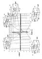
第2の実施の形態に係る帯域除去フィルタ(以下、フィルタ200という)の構成を図7を参照しつつ説明する。図7は、フィルタ200の構成を示す図である。
第3の実施の形態に係る帯域除去フィルタ(以下、フィルタ300という)の構成を図8および図9を参照しつつ説明する。
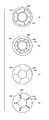
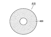
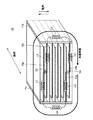
第4の実施の形態に係る帯域除去フィルタ(以下、フィルタ400という)の構成を図10、図11、図12を参照しつつ説明する。
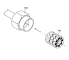
第1の実施の形態から第4の実施の形態で説明した帯域除去フィルタは、いずれも、コネクタに実装することができる。
Claims (14)
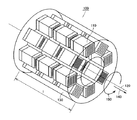
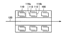
- 信号ライン(120)を流れる電流の特定の周波数成分を除去する帯域除去フィルタであって、
前記信号ライン(120)を軸として放射状に配置されたメタマテリアル(110)を備え、
前記メタマテリアル(110)は、前記周波数成分における透磁率が負になるように配置されている帯域除去フィルタ。 - 前記メタマテリアル(110)は、
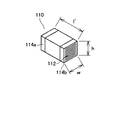
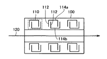
各々が絶縁物を介して互いに対向する第1および第2電極からなる複数の電極対(112)と、
前記第1および第2電極を電気的に接続する接続体とを含み、
前記第1および第2電極の各電極面は、前記電流によって形成される磁力線に対して実質的に平行となるように配置されている、請求の範囲第1項に記載の帯域除去フィルタ。 - 前記接続体は、前記電流によって形成される磁力線が前記第1および第2電極で挟まれた空間を通過することを妨げないように配置されている、請求の範囲第2項に記載の帯域除去フィルタ。
- 前記接続体は、平行に対向して形成された2つの外部電極(114a,114b)からなり、
前記2つの外部電極(114a,114b)の各電極面は、前記電流によって形成される磁力線に対し実質的に平行となるように配置されている、請求の範囲第3項に記載の帯域除去フィルタ。 - 前記メタマテリアル(110)は、
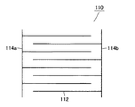
絶縁物を介して互いに平行に配置された複数の平板電極(112)と、
前記複数の平板電極の偶数番目の平板電極と電気的に接続された第1接続電極(114a)と、
前記複数の平板電極の奇数番目の平板電極と電気的に接続された第2接続電極(114b)とを含み、
前記第1および第2接続電極(114a,114b)の各電極面は、前記複数の平板電極(112)の電極面に対して垂直に形成され、
前記複数の平板電極(112)の各電極面は、前記電流によって形成される磁力線に対して実質的に平行となるように配置されている、請求の範囲第1項に記載の帯域除去フィルタ。 - 前記信号ライン(120)に対し垂直に立設されたドーナツ板(210)をさらに備え、
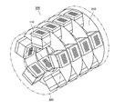
前記メタマテリアル(110)は前記ドーナツ板(210)上に固定されている、請求の範囲第5項に記載の帯域除去フィルタ。 - 前記メタマテリアル(110)は、
各々が互いに平行する複数の電極面を有する第1くし型電極(114a,112)および第2くし型電極(114b,112)を含み、
前記第1くし型電極(114a,112)の最上層の電極面と前記第2くし型電極(114b,112)の最上層の電極面とが所定の間隔をもって平行に対向するように形成され、かつ、前記第1くし型電極(114a,112)の最下層の電極面と前記第2くし型電極(114b,112)の最下層の電極面とが所定の間隔をもって平行に対向するように形成され、
前記第1くし型電極(114a,112)および第2くし型電極(114b,112)の各電極面は、前記電流によって形成される磁力線に対して実質的に平行となるように配置されている、請求の範囲第1項に記載の帯域除去フィルタ。 - 前記信号ライン(120)に対し垂直に立設されたドーナツ板(210)をさらに備え、
前記メタマテリアル(110)は前記ドーナツ板(210)上に固定されている、請求の範囲第7項に記載の帯域除去フィルタ。 - 前記メタマテリアル(110)は、
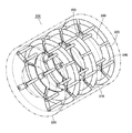
前記信号ライン(120)を軸とし、互いに径が異なる円筒面である複数の円筒型電極(420)と、
前記複数の円筒型電極(420)の偶数番目の円筒型電極と電気的に接続された第1接続電極(430a)と、
前記複数の円筒型電極(420)の奇数番目の円筒型電極と電気的に接続された第2接続電極(430b)とを含む、請求の範囲第1項に記載の帯域除去フィルタ。 - 前記メタマテリアル(110)は、複数の基材(310)から成り、
前記基材(310)には、
各々が絶縁物を介して互いに対向する第1および第2電極(310,320)と、
前記第1および第2電極(310,320)を電気的に接続する接続体(340,350)とが形成されている、請求の範囲第1項に記載の帯域除去フィルタ。 - 信号ライン(120)を流れる電流の特定の周波数成分を除去する帯域除去フィルタであって、
前記信号ライン(120)を軸として放射状に配置されたメタマテリアル(110)を備え、
前記メタマテリアル(110)は、
複数の第1電極(112)と、
前記複数の第1電極(112)のそれぞれに対向する複数の第2電極(112)と、
前記複数の第1電極(112)と前記複数の第2電極(112)とをそれぞれ電気的に接続する接続体(114a,114b)を含み、
各前記第1電極(112)および各前記第2電極(112)の電極面は、前記信号ライン(120)を軸として前記信号ライン(120)を取り囲むように配置されている、帯域除去フィルタ。 - 信号ライン(120)を流れる電流の特定の周波数成分を除去する帯域除去フィルタであって、
前記信号ライン(120)を軸として放射状に配置されたメタマテリアル(110)を備え、
前記メタマテリアル(110)は、
複数の第1電極(112)と、
前記複数の第1電極(112)のそれぞれに対向する複数の第2電極(112)と、
前記複数の第1電極(112)と前記複数の第2電極(112)とをそれぞれ電気的に接続する接続体(114a,114b)を含み、
各前記第1電極(112)および各前記第2電極(112)の電極面は、前記信号ライン(120)に直交するように配置されている、帯域除去フィルタ。 - 前記メタマテリアル(110)の前記信号ライン(120)に沿った長さは、前記所定の周波数成分に相当する1波長の1/4より短くなるように形成される、請求の範囲第1項に記載の帯域除去フィルタ。
- 請求の範囲第1項に記載の帯域除去フィルタを内蔵する帯域除去フィルタ付きコネクタ。
Priority Applications (1)
| Application Number | Priority Date | Filing Date | Title |
|---|---|---|---|
| JP2009546986A JP5218428B2 (ja) | 2007-12-21 | 2008-11-10 | 帯域除去フィルタおよび帯域除去フィルタ付きコネクタ |
Applications Claiming Priority (4)
| Application Number | Priority Date | Filing Date | Title |
|---|---|---|---|
| JP2007330513 | 2007-12-21 | ||
| JP2007330513 | 2007-12-21 | ||
| PCT/JP2008/070409 WO2009081663A1 (ja) | 2007-12-21 | 2008-11-10 | 帯域除去フィルタおよび帯域除去フィルタ付きコネクタ |
| JP2009546986A JP5218428B2 (ja) | 2007-12-21 | 2008-11-10 | 帯域除去フィルタおよび帯域除去フィルタ付きコネクタ |
Publications (2)
| Publication Number | Publication Date |
|---|---|
| JPWO2009081663A1 true JPWO2009081663A1 (ja) | 2011-05-06 |
| JP5218428B2 JP5218428B2 (ja) | 2013-06-26 |
Family
ID=40800979
Family Applications (1)
| Application Number | Title | Priority Date | Filing Date |
|---|---|---|---|
| JP2009546986A Expired - Fee Related JP5218428B2 (ja) | 2007-12-21 | 2008-11-10 | 帯域除去フィルタおよび帯域除去フィルタ付きコネクタ |
Country Status (2)
| Country | Link |
|---|---|
| JP (1) | JP5218428B2 (ja) |
| WO (1) | WO2009081663A1 (ja) |
Cited By (1)
| Publication number | Priority date | Publication date | Assignee | Title |
|---|---|---|---|---|
| US9754730B2 (en) * | 2015-03-13 | 2017-09-05 | Avx Corporation | Low profile multi-anode assembly in cylindrical housing |
Families Citing this family (5)
| Publication number | Priority date | Publication date | Assignee | Title |
|---|---|---|---|---|
| WO2009128310A1 (ja) * | 2008-04-18 | 2009-10-22 | 株式会社村田製作所 | 機能基板 |
| JP5304883B2 (ja) * | 2009-03-02 | 2013-10-02 | 株式会社村田製作所 | 電気部品、および、電気回路の部分構造 |
| JP5482915B2 (ja) * | 2011-02-10 | 2014-05-07 | 株式会社村田製作所 | メタマテリアル、電気装置、および、メタマテリアルを備えた電気装置 |
| JP2019033216A (ja) * | 2017-08-09 | 2019-02-28 | 株式会社Soken | フィルムコンデンサ及びその製造方法 |
| JP6775232B1 (ja) * | 2019-04-25 | 2020-10-28 | 地方独立行政法人大阪産業技術研究所 | 電子部材およびその製造方法 |
Family Cites Families (4)
| Publication number | Priority date | Publication date | Assignee | Title |
|---|---|---|---|---|
| US4424551B1 (en) * | 1982-01-25 | 1991-06-11 | Highly-reliable feed through/filter capacitor and method for making same | |
| KR100495871B1 (ko) * | 1999-04-23 | 2005-06-16 | 익스팬테크주식회사 | 각형 소자를 내장한 관통형 필터 |
| JP4669744B2 (ja) * | 2005-06-20 | 2011-04-13 | 独立行政法人理化学研究所 | 光学材料、それを用いた光学素子およびその作製方法 |
| JP4535995B2 (ja) * | 2005-12-05 | 2010-09-01 | 日本電気株式会社 | 多層プリント回路基板のビア構造、それを有する帯域阻止フィルタ |
-
2008
- 2008-11-10 WO PCT/JP2008/070409 patent/WO2009081663A1/ja not_active Ceased
- 2008-11-10 JP JP2009546986A patent/JP5218428B2/ja not_active Expired - Fee Related
Cited By (1)
| Publication number | Priority date | Publication date | Assignee | Title |
|---|---|---|---|---|
| US9754730B2 (en) * | 2015-03-13 | 2017-09-05 | Avx Corporation | Low profile multi-anode assembly in cylindrical housing |
Also Published As
| Publication number | Publication date |
|---|---|
| WO2009081663A1 (ja) | 2009-07-02 |
| JP5218428B2 (ja) | 2013-06-26 |
Similar Documents
| Publication | Publication Date | Title |
|---|---|---|
| JP5440504B2 (ja) | メタマテリアル | |
| JP5287862B2 (ja) | メタマテリアル | |
| JP5218428B2 (ja) | 帯域除去フィルタおよび帯域除去フィルタ付きコネクタ | |
| US8222975B2 (en) | Transmission line resonator, high-frequency filter using the same, high-frequency module, and radio device | |
| JP6551305B2 (ja) | 積層インダクタ | |
| JP5516581B2 (ja) | アンテナおよびアンテナモジュール | |
| JP5019033B2 (ja) | コモンモード電流抑制ebgフィルタ | |
| CN110024283B (zh) | Lc谐振器以及lc滤波器 | |
| WO2011114859A1 (ja) | コモンモードフィルタ用インダクタおよびコモンモードフィルタ | |
| JP2015534760A (ja) | 電磁吸収体 | |
| JP5104879B2 (ja) | 共振器およびそれを備える基板、ならびに共振を生じさせる方法 | |
| JP2017212350A (ja) | 電子部品 | |
| US8576027B2 (en) | Differential-common mode resonant filters | |
| JP2015111784A (ja) | 積層帯域除去フィルタ | |
| JP2006024772A (ja) | コモンモードノイズフィルタ | |
| JP5218551B2 (ja) | 機能基板 | |
| JP2017225086A (ja) | 誘電体フィルタ | |
| JP2009088329A (ja) | コイル部品 | |
| JP2014003090A (ja) | 回路基板 | |
| JP5304883B2 (ja) | 電気部品、および、電気回路の部分構造 | |
| JP2005347379A (ja) | コモンモードフィルタ | |
| JP6911932B2 (ja) | 偏波制御板 | |
| JP7234583B2 (ja) | 電磁波クローキング構造体 | |
| EP1512157A1 (en) | Decoupling module for decoupling high-frequency signals from a power supply line | |
| JP2012010150A (ja) | 電気部品、電気回路基板、インピーダンス整合方法、および、電気回路の部分構造 |
Legal Events
| Date | Code | Title | Description |
|---|---|---|---|
| A131 | Notification of reasons for refusal |
Free format text: JAPANESE INTERMEDIATE CODE: A131 Effective date: 20120821 |
|
| A521 | Request for written amendment filed |
Free format text: JAPANESE INTERMEDIATE CODE: A523 Effective date: 20121005 |
|
| A131 | Notification of reasons for refusal |
Free format text: JAPANESE INTERMEDIATE CODE: A131 Effective date: 20121106 |
|
| A521 | Request for written amendment filed |
Free format text: JAPANESE INTERMEDIATE CODE: A523 Effective date: 20130104 |
|
| TRDD | Decision of grant or rejection written | ||
| A01 | Written decision to grant a patent or to grant a registration (utility model) |
Free format text: JAPANESE INTERMEDIATE CODE: A01 Effective date: 20130205 |
|
| A61 | First payment of annual fees (during grant procedure) |
Free format text: JAPANESE INTERMEDIATE CODE: A61 Effective date: 20130218 |
|
| FPAY | Renewal fee payment (event date is renewal date of database) |
Free format text: PAYMENT UNTIL: 20160315 Year of fee payment: 3 |
|
| R150 | Certificate of patent or registration of utility model |
Ref document number: 5218428 Country of ref document: JP Free format text: JAPANESE INTERMEDIATE CODE: R150 Free format text: JAPANESE INTERMEDIATE CODE: R150 |
|
| LAPS | Cancellation because of no payment of annual fees |