JPWO2012144147A1 - 縦型ゲート半導体装置およびその製造方法 - Google Patents
縦型ゲート半導体装置およびその製造方法 Download PDFInfo
- Publication number
- JPWO2012144147A1 JPWO2012144147A1 JP2013510861A JP2013510861A JPWO2012144147A1 JP WO2012144147 A1 JPWO2012144147 A1 JP WO2012144147A1 JP 2013510861 A JP2013510861 A JP 2013510861A JP 2013510861 A JP2013510861 A JP 2013510861A JP WO2012144147 A1 JPWO2012144147 A1 JP WO2012144147A1
- Authority
- JP
- Japan
- Prior art keywords
- insulating film
- trench
- region
- source region
- semiconductor device
- Prior art date
- Legal status (The legal status is an assumption and is not a legal conclusion. Google has not performed a legal analysis and makes no representation as to the accuracy of the status listed.)
- Granted
Links
Images











Classifications
-
- H—ELECTRICITY
- H10—SEMICONDUCTOR DEVICES; ELECTRIC SOLID-STATE DEVICES NOT OTHERWISE PROVIDED FOR
- H10D—INORGANIC ELECTRIC SEMICONDUCTOR DEVICES
- H10D30/00—Field-effect transistors [FET]
- H10D30/01—Manufacture or treatment
- H10D30/021—Manufacture or treatment of FETs having insulated gates [IGFET]
- H10D30/025—Manufacture or treatment of FETs having insulated gates [IGFET] of vertical IGFETs
-
- H—ELECTRICITY
- H10—SEMICONDUCTOR DEVICES; ELECTRIC SOLID-STATE DEVICES NOT OTHERWISE PROVIDED FOR
- H10D—INORGANIC ELECTRIC SEMICONDUCTOR DEVICES
- H10D30/00—Field-effect transistors [FET]
- H10D30/01—Manufacture or treatment
- H10D30/021—Manufacture or treatment of FETs having insulated gates [IGFET]
- H10D30/028—Manufacture or treatment of FETs having insulated gates [IGFET] of double-diffused metal oxide semiconductor [DMOS] FETs
- H10D30/0291—Manufacture or treatment of FETs having insulated gates [IGFET] of double-diffused metal oxide semiconductor [DMOS] FETs of vertical DMOS [VDMOS] FETs
- H10D30/0297—Manufacture or treatment of FETs having insulated gates [IGFET] of double-diffused metal oxide semiconductor [DMOS] FETs of vertical DMOS [VDMOS] FETs using recessing of the gate electrodes, e.g. to form trench gate electrodes
-
- H—ELECTRICITY
- H10—SEMICONDUCTOR DEVICES; ELECTRIC SOLID-STATE DEVICES NOT OTHERWISE PROVIDED FOR
- H10D—INORGANIC ELECTRIC SEMICONDUCTOR DEVICES
- H10D30/00—Field-effect transistors [FET]
- H10D30/60—Insulated-gate field-effect transistors [IGFET]
- H10D30/64—Double-diffused metal-oxide semiconductor [DMOS] FETs
- H10D30/66—Vertical DMOS [VDMOS] FETs
- H10D30/668—Vertical DMOS [VDMOS] FETs having trench gate electrodes, e.g. UMOS transistors
-
- H—ELECTRICITY
- H10—SEMICONDUCTOR DEVICES; ELECTRIC SOLID-STATE DEVICES NOT OTHERWISE PROVIDED FOR
- H10D—INORGANIC ELECTRIC SEMICONDUCTOR DEVICES
- H10D62/00—Semiconductor bodies, or regions thereof, of devices having potential barriers
- H10D62/10—Shapes, relative sizes or dispositions of the regions of the semiconductor bodies; Shapes of the semiconductor bodies
- H10D62/13—Semiconductor regions connected to electrodes carrying current to be rectified, amplified or switched, e.g. source or drain regions
- H10D62/149—Source or drain regions of field-effect devices
- H10D62/151—Source or drain regions of field-effect devices of IGFETs
- H10D62/152—Source regions of DMOS transistors
- H10D62/153—Impurity concentrations or distributions
-
- H—ELECTRICITY
- H10—SEMICONDUCTOR DEVICES; ELECTRIC SOLID-STATE DEVICES NOT OTHERWISE PROVIDED FOR
- H10D—INORGANIC ELECTRIC SEMICONDUCTOR DEVICES
- H10D62/00—Semiconductor bodies, or regions thereof, of devices having potential barriers
- H10D62/10—Shapes, relative sizes or dispositions of the regions of the semiconductor bodies; Shapes of the semiconductor bodies
- H10D62/13—Semiconductor regions connected to electrodes carrying current to be rectified, amplified or switched, e.g. source or drain regions
- H10D62/149—Source or drain regions of field-effect devices
- H10D62/151—Source or drain regions of field-effect devices of IGFETs
- H10D62/152—Source regions of DMOS transistors
- H10D62/154—Dispositions
-
- H—ELECTRICITY
- H10—SEMICONDUCTOR DEVICES; ELECTRIC SOLID-STATE DEVICES NOT OTHERWISE PROVIDED FOR
- H10D—INORGANIC ELECTRIC SEMICONDUCTOR DEVICES
- H10D62/00—Semiconductor bodies, or regions thereof, of devices having potential barriers
- H10D62/10—Shapes, relative sizes or dispositions of the regions of the semiconductor bodies; Shapes of the semiconductor bodies
- H10D62/13—Semiconductor regions connected to electrodes carrying current to be rectified, amplified or switched, e.g. source or drain regions
- H10D62/149—Source or drain regions of field-effect devices
- H10D62/151—Source or drain regions of field-effect devices of IGFETs
- H10D62/152—Source regions of DMOS transistors
- H10D62/155—Shapes
-
- H—ELECTRICITY
- H10—SEMICONDUCTOR DEVICES; ELECTRIC SOLID-STATE DEVICES NOT OTHERWISE PROVIDED FOR
- H10D—INORGANIC ELECTRIC SEMICONDUCTOR DEVICES
- H10D62/00—Semiconductor bodies, or regions thereof, of devices having potential barriers
- H10D62/10—Shapes, relative sizes or dispositions of the regions of the semiconductor bodies; Shapes of the semiconductor bodies
- H10D62/17—Semiconductor regions connected to electrodes not carrying current to be rectified, amplified or switched, e.g. channel regions
- H10D62/393—Body regions of DMOS transistors or IGBTs
-
- H—ELECTRICITY
- H10—SEMICONDUCTOR DEVICES; ELECTRIC SOLID-STATE DEVICES NOT OTHERWISE PROVIDED FOR
- H10D—INORGANIC ELECTRIC SEMICONDUCTOR DEVICES
- H10D64/00—Electrodes of devices having potential barriers
- H10D64/01—Manufacture or treatment
- H10D64/013—Manufacture or treatment of electrodes having a conductor capacitively coupled to a semiconductor by an insulator
- H10D64/01302—Manufacture or treatment of electrodes having a conductor capacitively coupled to a semiconductor by an insulator the insulator being formed after the semiconductor body, the semiconductor being silicon
- H10D64/01304—Manufacture or treatment of electrodes having a conductor capacitively coupled to a semiconductor by an insulator the insulator being formed after the semiconductor body, the semiconductor being silicon characterised by the conductor
- H10D64/01306—Manufacture or treatment of electrodes having a conductor capacitively coupled to a semiconductor by an insulator the insulator being formed after the semiconductor body, the semiconductor being silicon characterised by the conductor the conductor comprising a layer of silicon contacting the insulator, e.g. polysilicon
-
- H—ELECTRICITY
- H10—SEMICONDUCTOR DEVICES; ELECTRIC SOLID-STATE DEVICES NOT OTHERWISE PROVIDED FOR
- H10D—INORGANIC ELECTRIC SEMICONDUCTOR DEVICES
- H10D64/00—Electrodes of devices having potential barriers
- H10D64/20—Electrodes characterised by their shapes, relative sizes or dispositions
- H10D64/27—Electrodes not carrying the current to be rectified, amplified, oscillated or switched, e.g. gates
- H10D64/311—Gate electrodes for field-effect devices
- H10D64/411—Gate electrodes for field-effect devices for FETs
- H10D64/511—Gate electrodes for field-effect devices for FETs for IGFETs
- H10D64/512—Disposition of the gate electrodes, e.g. buried gates
- H10D64/513—Disposition of the gate electrodes, e.g. buried gates within recesses in the substrate, e.g. trench gates, groove gates or buried gates
-
- H—ELECTRICITY
- H10—SEMICONDUCTOR DEVICES; ELECTRIC SOLID-STATE DEVICES NOT OTHERWISE PROVIDED FOR
- H10P—GENERIC PROCESSES OR APPARATUS FOR THE MANUFACTURE OR TREATMENT OF DEVICES COVERED BY CLASS H10
- H10P30/00—Ion implantation into wafers, substrates or parts of devices
- H10P30/20—Ion implantation into wafers, substrates or parts of devices into semiconductor materials, e.g. for doping
- H10P30/202—Ion implantation into wafers, substrates or parts of devices into semiconductor materials, e.g. for doping characterised by the semiconductor materials
- H10P30/204—Ion implantation into wafers, substrates or parts of devices into semiconductor materials, e.g. for doping characterised by the semiconductor materials into Group IV semiconductors
-
- H—ELECTRICITY
- H10—SEMICONDUCTOR DEVICES; ELECTRIC SOLID-STATE DEVICES NOT OTHERWISE PROVIDED FOR
- H10P—GENERIC PROCESSES OR APPARATUS FOR THE MANUFACTURE OR TREATMENT OF DEVICES COVERED BY CLASS H10
- H10P30/00—Ion implantation into wafers, substrates or parts of devices
- H10P30/20—Ion implantation into wafers, substrates or parts of devices into semiconductor materials, e.g. for doping
- H10P30/21—Ion implantation into wafers, substrates or parts of devices into semiconductor materials, e.g. for doping of electrically active species
- H10P30/212—Through-implantation
-
- H—ELECTRICITY
- H10—SEMICONDUCTOR DEVICES; ELECTRIC SOLID-STATE DEVICES NOT OTHERWISE PROVIDED FOR
- H10P—GENERIC PROCESSES OR APPARATUS FOR THE MANUFACTURE OR TREATMENT OF DEVICES COVERED BY CLASS H10
- H10P30/00—Ion implantation into wafers, substrates or parts of devices
- H10P30/20—Ion implantation into wafers, substrates or parts of devices into semiconductor materials, e.g. for doping
- H10P30/22—Ion implantation into wafers, substrates or parts of devices into semiconductor materials, e.g. for doping using masks
-
- H—ELECTRICITY
- H10—SEMICONDUCTOR DEVICES; ELECTRIC SOLID-STATE DEVICES NOT OTHERWISE PROVIDED FOR
- H10P—GENERIC PROCESSES OR APPARATUS FOR THE MANUFACTURE OR TREATMENT OF DEVICES COVERED BY CLASS H10
- H10P50/00—Etching of wafers, substrates or parts of devices
- H10P50/20—Dry etching; Plasma etching; Reactive-ion etching
- H10P50/26—Dry etching; Plasma etching; Reactive-ion etching of conductive or resistive materials
- H10P50/264—Dry etching; Plasma etching; Reactive-ion etching of conductive or resistive materials by chemical means
-
- H—ELECTRICITY
- H10—SEMICONDUCTOR DEVICES; ELECTRIC SOLID-STATE DEVICES NOT OTHERWISE PROVIDED FOR
- H10P—GENERIC PROCESSES OR APPARATUS FOR THE MANUFACTURE OR TREATMENT OF DEVICES COVERED BY CLASS H10
- H10P52/00—Grinding, lapping or polishing of wafers, substrates or parts of devices
- H10P52/40—Chemomechanical polishing [CMP]
- H10P52/403—Chemomechanical polishing [CMP] of conductive or resistive materials
Landscapes
- Electrodes Of Semiconductors (AREA)
- Chemical & Material Sciences (AREA)
- Chemical Kinetics & Catalysis (AREA)
- General Chemical & Material Sciences (AREA)
- Insulated Gate Type Field-Effect Transistor (AREA)
Abstract
Description
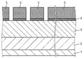
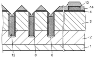
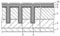
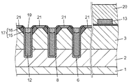
2,102 ドレイン領域
3,103 ボディー領域(第1ボディー領域)
4 シリコン酸化膜
5 レジストパターン
6,105,111 トレンチ
7 シリコン酸化膜
8,106 ゲート絶縁膜
9 ポリシリコン膜
10 キャップ絶縁膜
11 レジストパターン
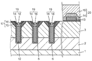
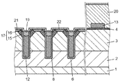
12,107 ゲート電極
13 ポリシリコン配線
14 第1絶縁膜
15 第1ソース領域
16 第2ソース領域
17,112 ソース領域
18 第2絶縁膜
19 埋込絶縁膜
20,110 層間絶縁膜
21,113 ボディーコンタクト領域(第2ボディー領域)
22 バリアメタル膜
23 金属膜(導電膜)
114 ソース電極
Claims (14)
- 縦型ゲート半導体装置の製造方法であって、
半導体基板の上に第1導電型のドレイン領域を形成する第1の工程と、
前記ドレイン領域の上に、前記第1導電型とは反対導電型である第2導電型の第1ボディー領域を形成し、前記半導体基板と前記ドレイン領域と前記第1ボディー領域とで基板を構成させる第2の工程と、
前記第1ボディー領域を貫通して前記ドレイン領域に達するトレンチを前記基板に形成する第3の工程と、
前記第3の工程の後に、前記トレンチの上部に凹部が残る状態で、前記トレンチ内にゲート電極を形成する第4の工程と、
前記第4の工程の後に、前記凹部に形成されるとともに、前記トレンチ両側の前記基板表面において、前記トレンチ端からの距離が離れるにつれて膜厚が増大する部分を有する、第1絶縁膜を形成する第5の工程と、
前記第5の工程の後に、前記第1絶縁膜を介した不純物導入により、前記トレンチに沿って配置された、前記トレンチと隣接するとともに前記ゲート電極の上部と隣接する、第1導電型の第1ソース領域を形成する第6の工程と、
前記第6の工程の後に、前記第1絶縁膜をエッチバックして、前記トレンチ両側の前記基板表面、および前記トレンチ側壁を露出させる第7の工程と、
前記第7の工程の後に、エッチバックされた前記第1絶縁膜を介した不純物導入により、前記第1ソース領域の上部に、前記トレンチに沿って配置された、第1導電型の第2ソース領域を形成する第8の工程と、
前記第8の工程の後に、前記第1絶縁膜を被覆する第2絶縁膜を形成する第9の工程と、
前記第1絶縁膜および前記第2絶縁膜により構成される積層絶縁膜をエッチングすることにより、前記ゲート電極上の前記トレンチ内に、前記積層絶縁膜の一部からなる埋込絶縁膜を形成するとともに、前記基板表面を露出させる第10の工程と、
前記露出した前記基板表面から不純物を導入することにより、前記第1ボディー領域の上側に、前記第2ソース領域と隣接して、第2導電型の第2ボディー領域を形成する第11の工程と、
前記第2ソース領域と前記第2ボディー領域とを電気的に接続する導電膜を形成する第12の工程と、
を有する縦型ゲート半導体装置の製造方法。 - 前記第4の工程が、
導電性ポリシリコン膜を形成する工程と、
前記導電性ポリシリコン膜上にキャップ絶縁膜を形成する工程と、
前記キャップ絶縁膜および前記導電性ポリシリコン膜を加工することにより、前記キャップ絶縁膜に被覆された導電性ポリシリコン膜からなる配線および前記ゲート電極とを形成する工程と、
を有する請求項1に記載の縦型ゲート半導体装置の製造方法。 - 前記第1絶縁膜の膜厚増大部分は、前記基板表面とのなす角度が30°から60°の傾斜を有する順テーパー形状である、請求項2に記載の縦型ゲート半導体装置の製造方法。
- 前記第6の工程において、前記第1絶縁膜は基板全面に形成され、
前記第1ソース領域を形成する不純物導入がイオン注入によってなされる、請求項3に記載の縦型ゲート半導体装置の製造方法。 - 前記第7の工程において、前記第1絶縁膜のエッチバックが、ドライエッチングまたはウエットエッチングによりなされる、請求項4に記載の縦型ゲート半導体装置の製造方法。
- 前記第8の工程において、前記第2ソース領域を形成する不純物導入がイオン注入によってなされる、請求項5に記載の縦型ゲート半導体装置の製造方法。
- 前記第9の工程と前記第10の工程との間に、CMPにより前記積層絶縁膜の表面を平坦化する工程をさらに有する、請求項6に記載の縦型ゲート半導体装置の製造方法。
- 前記第10の工程において、前記エッチングは、前記第2ボディー領域の形成予定領域上に形成された前記積層絶縁膜のエッチングレートが、前記ゲート電極上に形成された前記積層絶縁膜のエッチングレートよりも大きくなる条件で実施される、請求項7に記載の縦型ゲート半導体装置の製造方法。
- 前記第11の工程において、前記第2ボディー領域を形成する不純物導入がイオン注入によってなされる、請求項8に記載の縦型ゲート半導体装置の製造方法。
- 前記第11の工程と前記第12の工程との間に、前記ゲート電極上に残存する前記積層絶縁膜の一部をエッチング除去し、トレンチ側壁に前記第2ソース領域を露出させる工程をさらに有する、請求項9に記載の縦型ゲート半導体装置の製造方法。
- 前記トレンチ側壁に前記第2ソース領域を露出させる工程のエッチングが、前記第2ソース領域のトレンチ側壁の上端部が曲面に加工される条件で実施される、請求項10に記載の縦型ゲート半導体装置の製造方法。
- 半導体基板の上に設けられた第1導電型のドレイン領域と、
前記ドレイン領域の上に設けられた、前記第1導電型とは反対導電型である第2導電型の第1ボディー領域と、
前記半導体基板と前記ドレイン領域と前記第1ボディー領域とからなる基板と、
前記第1ボディー領域を貫通して前記ドレイン領域に達する状態で設けられたトレンチと、
前記トレンチ内に、トレンチの上端より低い位置に上面が位置する状態で設けられたゲート電極と、
前記第1ボディー領域の表面部に、前記ゲート電極の上部および前記トレンチと隣接して前記トレンチに沿って設けられた、表面から前記トレンチの深さ方向の距離が増大するにつれて前記トレンチの側壁に垂直な方向の不純物領域幅が減少し、かつ前記トレンチの側壁の上部に近づくにつれて不純物濃度が増大する、第1導電型の第1ソース領域と、
前記第1ソース領域の上部であって、前記トレンチ両側の前記基板表面および前記トレンチ側壁を含む領域に、前記トレンチに沿って配置された、前記第1ソース領域よりも高い不純物濃度を有する、第1導電型の第2ソース領域と、
前記第1ボディー領域の表面部に、前記第2ソース領域と隣接して前記第2ソース領域に沿って設けられた、前記第1ボディー領域よりも高い不純物濃度を有する、第2導電型の第2ボディー領域と、
前記ゲート電極の上の前記トレンチ内に設けられた埋込絶縁膜と、
前記第2ソース領域と前記第2ボディー領域とを電気的に接続する導電膜と、
を有する縦型ゲート半導体装置。 - 前記埋込絶縁膜は、少なくとも下部に前記第2ソース領域と同一種の不純物を含み、少なくとも上部に前記第2ボディー領域と同一種の不純物を含む、請求項12に記載の縦型ゲート半導体装置。
- 前記第1ソース領域と前記第1ボディー領域との界面が、前記トレンチの側壁に対して傾斜した平面状に構成される、請求項13に記載の縦型ゲート半導体装置。
Applications Claiming Priority (3)
| Application Number | Priority Date | Filing Date | Title |
|---|---|---|---|
| JP2011094415 | 2011-04-20 | ||
| JP2011094415 | 2011-04-20 | ||
| PCT/JP2012/002382 WO2012144147A1 (ja) | 2011-04-20 | 2012-04-05 | 縦型ゲート半導体装置およびその製造方法 |
Publications (2)
| Publication Number | Publication Date |
|---|---|
| JPWO2012144147A1 true JPWO2012144147A1 (ja) | 2014-07-28 |
| JP6031681B2 JP6031681B2 (ja) | 2016-11-24 |
Family
ID=47041282
Family Applications (1)
| Application Number | Title | Priority Date | Filing Date |
|---|---|---|---|
| JP2013510861A Active JP6031681B2 (ja) | 2011-04-20 | 2012-04-05 | 縦型ゲート半導体装置およびその製造方法 |
Country Status (3)
| Country | Link |
|---|---|
| US (3) | US20130037881A1 (ja) |
| JP (1) | JP6031681B2 (ja) |
| WO (1) | WO2012144147A1 (ja) |
Families Citing this family (17)
| Publication number | Priority date | Publication date | Assignee | Title |
|---|---|---|---|---|
| JP5616720B2 (ja) * | 2010-08-30 | 2014-10-29 | セイコーインスツル株式会社 | 半導体装置およびその製造方法 |
| KR20130107490A (ko) * | 2012-03-22 | 2013-10-02 | 에스케이하이닉스 주식회사 | 반도체 소자 및 그 제조 방법 |
| US9666663B2 (en) * | 2013-08-09 | 2017-05-30 | Infineon Technologies Ag | Semiconductor device with cell trench structures and contacts and method of manufacturing a semiconductor device |
| CN104916686A (zh) * | 2014-03-12 | 2015-09-16 | 北大方正集团有限公司 | 一种vdmos器件及其制造方法 |
| KR102164542B1 (ko) | 2014-05-21 | 2020-10-12 | 삼성전자 주식회사 | 매립형 게이트 구조체를 갖는 반도체 소자 및 그 제조 방법 |
| US20160329213A1 (en) * | 2015-05-04 | 2016-11-10 | Lam Research Corporation | Highly selective deposition of amorphous carbon as a metal diffusion barrier layer |
| US9954109B2 (en) | 2016-05-05 | 2018-04-24 | International Business Machines Corporation | Vertical transistor including controlled gate length and a self-aligned junction |
| US10727326B2 (en) * | 2017-08-21 | 2020-07-28 | Semiconductor Components Industries, Llc | Trench-gate insulated-gate bipolar transistors (IGBTs) |
| JP2019175930A (ja) * | 2018-03-27 | 2019-10-10 | エイブリック株式会社 | 半導体装置及びその製造方法 |
| US11239342B2 (en) | 2018-06-28 | 2022-02-01 | International Business Machines Corporation | Vertical transistors having improved control of top source or drain junctions |
| US10840106B2 (en) * | 2018-10-11 | 2020-11-17 | Oepic Semiconductors, Inc. | Planarization and flip-chip fabrication process of fine-line-geometry features with high-roughness metal-alloyed surfaces |
| DE102019101304B4 (de) * | 2019-01-18 | 2023-04-27 | Infineon Technologies Dresden GmbH & Co. KG | Leistungshalbleitervorrichtung und Verfahren zum Bilden einer Leistungshalbleitervorrichtung |
| CN112086454B (zh) * | 2019-06-14 | 2024-12-06 | 长鑫存储技术有限公司 | 半导体器件及其制备方法 |
| CN113241374B (zh) * | 2021-05-19 | 2023-07-14 | 深圳真茂佳半导体有限公司 | 功率晶体管结构及其制造方法 |
| CN113241372B (zh) * | 2021-05-19 | 2022-09-06 | 深圳真茂佳半导体有限公司 | 自对准功率场效应管的制备方法与结构 |
| JP7742791B2 (ja) * | 2022-03-11 | 2025-09-22 | ルネサスエレクトロニクス株式会社 | 半導体装置およびその製造方法 |
| KR102764893B1 (ko) * | 2022-07-19 | 2025-02-11 | 한국과학기술원 | 반도체 소자의 다중 패터닝 방법 |
Family Cites Families (33)
| Publication number | Priority date | Publication date | Assignee | Title |
|---|---|---|---|---|
| KR100218260B1 (ko) * | 1997-01-14 | 1999-09-01 | 김덕중 | 트랜치 게이트형 모스트랜지스터의 제조방법 |
| JP3502531B2 (ja) * | 1997-08-28 | 2004-03-02 | 株式会社ルネサステクノロジ | 半導体装置の製造方法 |
| US7084456B2 (en) * | 1999-05-25 | 2006-08-01 | Advanced Analogic Technologies, Inc. | Trench MOSFET with recessed clamping diode using graded doping |
| JP3215686B2 (ja) * | 1999-08-25 | 2001-10-09 | 株式会社日立製作所 | 半導体装置及びその製造方法 |
| JP2001085685A (ja) * | 1999-09-13 | 2001-03-30 | Shindengen Electric Mfg Co Ltd | トランジスタ |
| JP4091242B2 (ja) | 1999-10-18 | 2008-05-28 | セイコーインスツル株式会社 | 縦形mosトランジスタ及びその製造方法 |
| US6916745B2 (en) | 2003-05-20 | 2005-07-12 | Fairchild Semiconductor Corporation | Structure and method for forming a trench MOSFET having self-aligned features |
| JP4016781B2 (ja) * | 2002-09-25 | 2007-12-05 | 富士電機デバイステクノロジー株式会社 | 半導体素子の製造方法 |
| US6861701B2 (en) * | 2003-03-05 | 2005-03-01 | Advanced Analogic Technologies, Inc. | Trench power MOSFET with planarized gate bus |
| JP2005026391A (ja) * | 2003-07-01 | 2005-01-27 | Sanyo Electric Co Ltd | Mos型半導体装置 |
| JP4829473B2 (ja) | 2004-01-21 | 2011-12-07 | オンセミコンダクター・トレーディング・リミテッド | 絶縁ゲート型半導体装置およびその製造方法 |
| JP3999225B2 (ja) * | 2004-01-27 | 2007-10-31 | 松下電器産業株式会社 | 半導体装置およびその製造方法 |
| US7372088B2 (en) | 2004-01-27 | 2008-05-13 | Matsushita Electric Industrial Co., Ltd. | Vertical gate semiconductor device and method for fabricating the same |
| JP4232645B2 (ja) * | 2004-01-29 | 2009-03-04 | 富士電機デバイステクノロジー株式会社 | トレンチ横型半導体装置およびその製造方法 |
| US7400014B2 (en) * | 2004-04-20 | 2008-07-15 | International Rectifier Corporation | ACCUFET with schottky source contact |
| JP4841123B2 (ja) * | 2004-07-28 | 2011-12-21 | パナソニック株式会社 | 半導体記憶装置及びその製造方法 |
| JP2006073971A (ja) * | 2004-08-04 | 2006-03-16 | Sanken Electric Co Ltd | 半導体素子及び半導体素子の製造方法 |
| US7465986B2 (en) * | 2004-08-27 | 2008-12-16 | International Rectifier Corporation | Power semiconductor device including insulated source electrodes inside trenches |
| JP2006120894A (ja) * | 2004-10-22 | 2006-05-11 | Toshiba Corp | 半導体装置 |
| DE102004057237B4 (de) | 2004-11-26 | 2007-02-08 | Infineon Technologies Ag | Verfahren zum Herstellen von Kontaktlöchern in einem Halbleiterkörper sowie Transistor mit vertikalem Aufbau |
| CN1812127A (zh) * | 2004-12-14 | 2006-08-02 | 松下电器产业株式会社 | 纵型栅极半导体装置及其制造方法 |
| US7573096B2 (en) * | 2005-02-16 | 2009-08-11 | Shindengen Electric Manufacturing Co, Ltd. | Semiconductor device for reducing forward voltage by using OHMIC contact |
| JP2006332231A (ja) * | 2005-05-25 | 2006-12-07 | Sanyo Electric Co Ltd | 半導体装置の製造方法 |
| CN101548386B (zh) * | 2006-12-04 | 2011-11-09 | 三垦电气株式会社 | 绝缘栅型场效应晶体管及其制造方法 |
| US8067797B2 (en) * | 2007-10-17 | 2011-11-29 | International Rectifier Corporation | Variable threshold trench IGBT with offset emitter contacts |
| JP4877286B2 (ja) * | 2008-07-08 | 2012-02-15 | 株式会社デンソー | 炭化珪素半導体装置およびその製造方法 |
| US8642459B2 (en) * | 2008-08-28 | 2014-02-04 | Infineon Technologies Ag | Method for forming a semiconductor device with an isolation region on a gate electrode |
| US7851312B2 (en) * | 2009-01-23 | 2010-12-14 | Semiconductor Components Industries, Llc | Semiconductor component and method of manufacture |
| WO2011087994A2 (en) * | 2010-01-12 | 2011-07-21 | Maxpower Semiconductor Inc. | Devices, components and methods combining trench field plates with immobile electrostatic charge |
| US8378392B2 (en) * | 2010-04-07 | 2013-02-19 | Force Mos Technology Co., Ltd. | Trench MOSFET with body region having concave-arc shape |
| JP2012124425A (ja) * | 2010-12-10 | 2012-06-28 | Panasonic Corp | 縦型ゲート半導体装置の製造方法および縦型ゲート半導体装置 |
| US8580667B2 (en) * | 2010-12-14 | 2013-11-12 | Alpha And Omega Semiconductor Incorporated | Self aligned trench MOSFET with integrated diode |
| JP5661583B2 (ja) * | 2011-09-21 | 2015-01-28 | 株式会社東芝 | 半導体装置の製造方法 |
-
2012
- 2012-04-05 JP JP2013510861A patent/JP6031681B2/ja active Active
- 2012-04-05 WO PCT/JP2012/002382 patent/WO2012144147A1/ja not_active Ceased
- 2012-10-17 US US13/653,512 patent/US20130037881A1/en not_active Abandoned
-
2014
- 2014-09-26 US US14/497,615 patent/US9324837B2/en active Active
-
2016
- 2016-03-18 US US15/075,078 patent/US9853126B2/en active Active
Also Published As
| Publication number | Publication date |
|---|---|
| US20160204248A1 (en) | 2016-07-14 |
| US9853126B2 (en) | 2017-12-26 |
| US20150011066A1 (en) | 2015-01-08 |
| JP6031681B2 (ja) | 2016-11-24 |
| US20130037881A1 (en) | 2013-02-14 |
| US9324837B2 (en) | 2016-04-26 |
| WO2012144147A1 (ja) | 2012-10-26 |
Similar Documents
| Publication | Publication Date | Title |
|---|---|---|
| JP6031681B2 (ja) | 縦型ゲート半導体装置およびその製造方法 | |
| US8399957B2 (en) | Dual-depth self-aligned isolation structure for a back gate electrode | |
| CN102544100B (zh) | 带有集成二极管的自对准沟槽mosfet | |
| CN112133759B (zh) | 具有屏蔽栅沟槽结构的半导体器件及其制造方法 | |
| US20050173759A1 (en) | Fin FET and method of fabricating same | |
| US8507349B2 (en) | Semiconductor device employing fin-type gate and method for manufacturing the same | |
| KR20190032683A (ko) | 반도체 메모리 소자 및 그 제조 방법 | |
| JP6170812B2 (ja) | 半導体装置の製造方法 | |
| US8476136B2 (en) | Method and a structure for enhancing electrical insulation and dynamic performance of MIS structures comprising vertical field plates | |
| CN102339830A (zh) | 半导体器件及其制造方法 | |
| JP2008098593A (ja) | 半導体装置及びその製造方法 | |
| WO2006132284A1 (ja) | トレンチ型mosfet及びその製造方法 | |
| KR101832334B1 (ko) | 반도체소자 및 그 제조방법 | |
| JP2011243948A (ja) | 半導体装置及びその製造方法 | |
| US9431286B1 (en) | Deep trench with self-aligned sinker | |
| US8492221B2 (en) | Method for fabricating power semiconductor device with super junction structure | |
| US9818859B2 (en) | Quasi-vertical power MOSFET and methods of forming the same | |
| US20120056256A1 (en) | Semiconductor device and method for forming the same | |
| US20220278209A1 (en) | High voltage field effect transistors with metal-insulator-semiconductor contacts and method of making the same | |
| JP2012124425A (ja) | 縦型ゲート半導体装置の製造方法および縦型ゲート半導体装置 | |
| JP2012238773A (ja) | 縦型ゲート半導体装置およびその製造方法 | |
| JP5385567B2 (ja) | 半導体装置および半導体装置の製造方法 | |
| JP2010123721A (ja) | 半導体装置 | |
| CN105633160A (zh) | Soi器件及其制造方法 | |
| US20130049122A1 (en) | Semiconductor device and method of manufacturing the same |
Legal Events
| Date | Code | Title | Description |
|---|---|---|---|
| A521 | Request for written amendment filed |
Free format text: JAPANESE INTERMEDIATE CODE: A523 Effective date: 20140919 |
|
| A711 | Notification of change in applicant |
Free format text: JAPANESE INTERMEDIATE CODE: A711 Effective date: 20141006 |
|
| A621 | Written request for application examination |
Free format text: JAPANESE INTERMEDIATE CODE: A621 Effective date: 20141010 |
|
| A131 | Notification of reasons for refusal |
Free format text: JAPANESE INTERMEDIATE CODE: A131 Effective date: 20150203 |
|
| A521 | Request for written amendment filed |
Free format text: JAPANESE INTERMEDIATE CODE: A523 Effective date: 20150327 |
|
| A131 | Notification of reasons for refusal |
Free format text: JAPANESE INTERMEDIATE CODE: A131 Effective date: 20150818 |
|
| A521 | Request for written amendment filed |
Free format text: JAPANESE INTERMEDIATE CODE: A523 Effective date: 20151009 |
|
| RD01 | Notification of change of attorney |
Free format text: JAPANESE INTERMEDIATE CODE: A7421 Effective date: 20160519 |
|
| A131 | Notification of reasons for refusal |
Free format text: JAPANESE INTERMEDIATE CODE: A131 Effective date: 20160614 |
|
| A521 | Request for written amendment filed |
Free format text: JAPANESE INTERMEDIATE CODE: A523 Effective date: 20160727 |
|
| TRDD | Decision of grant or rejection written | ||
| A01 | Written decision to grant a patent or to grant a registration (utility model) |
Free format text: JAPANESE INTERMEDIATE CODE: A01 Effective date: 20160913 |
|
| A61 | First payment of annual fees (during grant procedure) |
Free format text: JAPANESE INTERMEDIATE CODE: A61 Effective date: 20160926 |
|
| R151 | Written notification of patent or utility model registration |
Ref document number: 6031681 Country of ref document: JP Free format text: JAPANESE INTERMEDIATE CODE: R151 |
|
| S111 | Request for change of ownership or part of ownership |
Free format text: JAPANESE INTERMEDIATE CODE: R313113 |
|
| SZ03 | Written request for cancellation of trust registration |
Free format text: JAPANESE INTERMEDIATE CODE: R313Z03 |
|
| R350 | Written notification of registration of transfer |
Free format text: JAPANESE INTERMEDIATE CODE: R350 |
|
| S111 | Request for change of ownership or part of ownership |
Free format text: JAPANESE INTERMEDIATE CODE: R313113 |
|
| R350 | Written notification of registration of transfer |
Free format text: JAPANESE INTERMEDIATE CODE: R350 |
|
| R250 | Receipt of annual fees |
Free format text: JAPANESE INTERMEDIATE CODE: R250 |
|
| R250 | Receipt of annual fees |
Free format text: JAPANESE INTERMEDIATE CODE: R250 |
|
| R250 | Receipt of annual fees |
Free format text: JAPANESE INTERMEDIATE CODE: R250 |
|
| R250 | Receipt of annual fees |
Free format text: JAPANESE INTERMEDIATE CODE: R250 |
|
| R250 | Receipt of annual fees |
Free format text: JAPANESE INTERMEDIATE CODE: R250 |
|
| R250 | Receipt of annual fees |
Free format text: JAPANESE INTERMEDIATE CODE: R250 |