JPWO2018190071A1 - Storage device - Google Patents
Storage device Download PDFInfo
- Publication number
- JPWO2018190071A1 JPWO2018190071A1 JP2019512395A JP2019512395A JPWO2018190071A1 JP WO2018190071 A1 JPWO2018190071 A1 JP WO2018190071A1 JP 2019512395 A JP2019512395 A JP 2019512395A JP 2019512395 A JP2019512395 A JP 2019512395A JP WO2018190071 A1 JPWO2018190071 A1 JP WO2018190071A1
- Authority
- JP
- Japan
- Prior art keywords
- layer
- element layer
- storage device
- intermediate electrode
- wiring layers
- Prior art date
- Legal status (The legal status is an assumption and is not a legal conclusion. Google has not performed a legal analysis and makes no representation as to the accuracy of the status listed.)
- Pending
Links
Images
Classifications
-
- H—ELECTRICITY
- H10—SEMICONDUCTOR DEVICES; ELECTRIC SOLID-STATE DEVICES NOT OTHERWISE PROVIDED FOR
- H10B—ELECTRONIC MEMORY DEVICES
- H10B63/00—Resistance change memory devices, e.g. resistive RAM [ReRAM] devices
- H10B63/80—Arrangements comprising multiple bistable or multi-stable switching components of the same type on a plane parallel to the substrate, e.g. cross-point arrays
- H10B63/84—Arrangements comprising multiple bistable or multi-stable switching components of the same type on a plane parallel to the substrate, e.g. cross-point arrays arranged in a direction perpendicular to the substrate, e.g. 3D cell arrays
-
- H—ELECTRICITY
- H10—SEMICONDUCTOR DEVICES; ELECTRIC SOLID-STATE DEVICES NOT OTHERWISE PROVIDED FOR
- H10D—INORGANIC ELECTRIC SEMICONDUCTOR DEVICES
- H10D84/00—Integrated devices formed in or on semiconductor substrates that comprise only semiconducting layers, e.g. on Si wafers or on GaAs-on-Si wafers
- H10D84/80—Integrated devices formed in or on semiconductor substrates that comprise only semiconducting layers, e.g. on Si wafers or on GaAs-on-Si wafers characterised by the integration of at least one component covered by groups H10D12/00 or H10D30/00, e.g. integration of IGFETs
-
- H—ELECTRICITY
- H10—SEMICONDUCTOR DEVICES; ELECTRIC SOLID-STATE DEVICES NOT OTHERWISE PROVIDED FOR
- H10B—ELECTRONIC MEMORY DEVICES
- H10B53/00—Ferroelectric RAM [FeRAM] devices comprising ferroelectric memory capacitors
- H10B53/20—Ferroelectric RAM [FeRAM] devices comprising ferroelectric memory capacitors characterised by the three-dimensional [3D] arrangements, e.g. with cells on different height levels
-
- H—ELECTRICITY
- H10—SEMICONDUCTOR DEVICES; ELECTRIC SOLID-STATE DEVICES NOT OTHERWISE PROVIDED FOR
- H10B—ELECTRONIC MEMORY DEVICES
- H10B53/00—Ferroelectric RAM [FeRAM] devices comprising ferroelectric memory capacitors
- H10B53/30—Ferroelectric RAM [FeRAM] devices comprising ferroelectric memory capacitors characterised by the memory core region
-
- H—ELECTRICITY
- H10—SEMICONDUCTOR DEVICES; ELECTRIC SOLID-STATE DEVICES NOT OTHERWISE PROVIDED FOR
- H10B—ELECTRONIC MEMORY DEVICES
- H10B61/00—Magnetic memory devices, e.g. magnetoresistive RAM [MRAM] devices
- H10B61/10—Magnetic memory devices, e.g. magnetoresistive RAM [MRAM] devices comprising components having two electrodes, e.g. diodes or MIM elements
-
- H—ELECTRICITY
- H10—SEMICONDUCTOR DEVICES; ELECTRIC SOLID-STATE DEVICES NOT OTHERWISE PROVIDED FOR
- H10B—ELECTRONIC MEMORY DEVICES
- H10B63/00—Resistance change memory devices, e.g. resistive RAM [ReRAM] devices
- H10B63/20—Resistance change memory devices, e.g. resistive RAM [ReRAM] devices comprising selection components having two electrodes, e.g. diodes
-
- H—ELECTRICITY
- H10—SEMICONDUCTOR DEVICES; ELECTRIC SOLID-STATE DEVICES NOT OTHERWISE PROVIDED FOR
- H10B—ELECTRONIC MEMORY DEVICES
- H10B63/00—Resistance change memory devices, e.g. resistive RAM [ReRAM] devices
- H10B63/20—Resistance change memory devices, e.g. resistive RAM [ReRAM] devices comprising selection components having two electrodes, e.g. diodes
- H10B63/22—Resistance change memory devices, e.g. resistive RAM [ReRAM] devices comprising selection components having two electrodes, e.g. diodes of the metal-insulator-metal type
-
- H—ELECTRICITY
- H10—SEMICONDUCTOR DEVICES; ELECTRIC SOLID-STATE DEVICES NOT OTHERWISE PROVIDED FOR
- H10B—ELECTRONIC MEMORY DEVICES
- H10B63/00—Resistance change memory devices, e.g. resistive RAM [ReRAM] devices
- H10B63/20—Resistance change memory devices, e.g. resistive RAM [ReRAM] devices comprising selection components having two electrodes, e.g. diodes
- H10B63/24—Resistance change memory devices, e.g. resistive RAM [ReRAM] devices comprising selection components having two electrodes, e.g. diodes of the Ovonic threshold switching type
-
- H—ELECTRICITY
- H10—SEMICONDUCTOR DEVICES; ELECTRIC SOLID-STATE DEVICES NOT OTHERWISE PROVIDED FOR
- H10B—ELECTRONIC MEMORY DEVICES
- H10B63/00—Resistance change memory devices, e.g. resistive RAM [ReRAM] devices
- H10B63/80—Arrangements comprising multiple bistable or multi-stable switching components of the same type on a plane parallel to the substrate, e.g. cross-point arrays
- H10B63/82—Arrangements comprising multiple bistable or multi-stable switching components of the same type on a plane parallel to the substrate, e.g. cross-point arrays the switching components having a common active material layer
-
- H—ELECTRICITY
- H10—SEMICONDUCTOR DEVICES; ELECTRIC SOLID-STATE DEVICES NOT OTHERWISE PROVIDED FOR
- H10B—ELECTRONIC MEMORY DEVICES
- H10B63/00—Resistance change memory devices, e.g. resistive RAM [ReRAM] devices
- H10B63/80—Arrangements comprising multiple bistable or multi-stable switching components of the same type on a plane parallel to the substrate, e.g. cross-point arrays
- H10B63/84—Arrangements comprising multiple bistable or multi-stable switching components of the same type on a plane parallel to the substrate, e.g. cross-point arrays arranged in a direction perpendicular to the substrate, e.g. 3D cell arrays
- H10B63/845—Arrangements comprising multiple bistable or multi-stable switching components of the same type on a plane parallel to the substrate, e.g. cross-point arrays arranged in a direction perpendicular to the substrate, e.g. 3D cell arrays the switching components being connected to a common vertical conductor
-
- H—ELECTRICITY
- H10—SEMICONDUCTOR DEVICES; ELECTRIC SOLID-STATE DEVICES NOT OTHERWISE PROVIDED FOR
- H10N—ELECTRIC SOLID-STATE DEVICES NOT OTHERWISE PROVIDED FOR
- H10N70/00—Solid-state devices having no potential barriers, and specially adapted for rectifying, amplifying, oscillating or switching
-
- H—ELECTRICITY
- H10—SEMICONDUCTOR DEVICES; ELECTRIC SOLID-STATE DEVICES NOT OTHERWISE PROVIDED FOR
- H10N—ELECTRIC SOLID-STATE DEVICES NOT OTHERWISE PROVIDED FOR
- H10N99/00—Subject matter not provided for in other groups of this subclass
-
- H—ELECTRICITY
- H10—SEMICONDUCTOR DEVICES; ELECTRIC SOLID-STATE DEVICES NOT OTHERWISE PROVIDED FOR
- H10W—GENERIC PACKAGES, INTERCONNECTIONS, CONNECTORS OR OTHER CONSTRUCTIONAL DETAILS OF DEVICES COVERED BY CLASS H10
- H10W20/00—Interconnections in chips, wafers or substrates
- H10W20/40—Interconnections external to wafers or substrates, e.g. back-end-of-line [BEOL] metallisations or vias connecting to gate electrodes
- H10W20/41—Interconnections external to wafers or substrates, e.g. back-end-of-line [BEOL] metallisations or vias connecting to gate electrodes characterised by their conductive parts
- H10W20/43—Layouts of interconnections
Landscapes
- Semiconductor Memories (AREA)
- Physics & Mathematics (AREA)
- Geometry (AREA)
- Mram Or Spin Memory Techniques (AREA)
Abstract
本開示の一実施形態の記憶装置は、一の方向に延伸する複数の第1の配線層と、他の方向に延伸する複数の第2の配線層と、複数の第1の配線層と複数の第2の配線層との対向領域にそれぞれ設けられた複数のメモリセルとを備え、複数のメモリセルはそれぞれ、選択素子層と、記憶素子層と、選択素子層と記憶素子層との間に設けられた中間電極層とを有し、選択素子層、記憶素子層および中間電極層のうちの少なくとも1つは、一の方向または他の方向に延伸して隣り合う複数のメモリセル間における共通層となっており、中間電極層は、非線形抵抗材料を含んで形成されている。A storage device according to an embodiment of the present disclosure includes a plurality of first wiring layers extending in one direction, a plurality of second wiring layers extending in another direction, a plurality of first wiring layers, and a plurality of first wiring layers. A plurality of memory cells provided in a region opposed to the second wiring layer, respectively, and the plurality of memory cells are each provided with a selection element layer, a storage element layer, and a storage element layer between the selection element layer and the storage element layer. And at least one of the selection element layer, the storage element layer, and the intermediate electrode layer extends in one direction or the other direction and is disposed between a plurality of adjacent memory cells. It is a common layer, and the intermediate electrode layer is formed including a nonlinear resistance material.
Description
本開示は、例えば、中間電極を間に選択素子および記憶素子が積層されたメモリセルを交差する配線の間に備えた記憶装置に関する。 The present disclosure relates to, for example, a storage device including an intermediate electrode between wirings crossing a memory cell in which a selection element and a storage element are stacked.
近年、メモリやストレージの大容量化および高速化が求められている。これに対して、不揮発性メモリの主流となっているフラッシュメモリでは、原理的な微細化の限界が近づいている。このため、磁気メモリや相変化メモリ、抵抗変化型メモリ等の新規メモリの開発が進められている。その中でも、相変化メモリおよび抵抗変化型メモリにおいて、選択素子と組み合わせたクロスポイント型メモリが提案されている。 In recent years, large capacity and high speed of memories and storages have been demanded. On the other hand, flash memories, which are the mainstream of non-volatile memories, are approaching the limit of miniaturization in principle. For this reason, new memories such as magnetic memories, phase change memories, and resistance change memories are being developed. Among them, a cross-point type memory combined with a selection element has been proposed for a phase change memory and a resistance change type memory.
クロスポイント型メモリは、交差する配線間の交点(クロスポイント)に、メモリ素子と選択素子とが直列に接続されたメモリセルが配置された構造となっている。具体的には、クロスポイント型メモリでは、互いに直交する2種類の配線層がそれぞれ複数配置され、その交点にメモリセルがそれぞれ形成されている。即ち、1つの配線層には複数のメモリセルが設けられており、換言すると、複数のメモリセルが1本の配線層を共有する構造となっている。 The cross point type memory has a structure in which a memory cell in which a memory element and a selection element are connected in series is arranged at an intersection (cross point) between intersecting wirings. Specifically, in the cross-point type memory, a plurality of two types of wiring layers which are orthogonal to each other are respectively arranged in plurality, and memory cells are formed at the intersections. That is, a plurality of memory cells are provided in one wiring layer, in other words, a structure in which a plurality of memory cells share one wiring layer.
このようなクロスポイント型メモリとしては、例えば特許文献1において、記憶素子材料とセル選択材料とを連続して成膜し、それらが複数の階層に渡って共有された3次元メモリアレイアーキテクチャが開示されている。特許文献2では、抵抗可変膜、導電層、整流絶縁膜を設け、1つの垂直電極に対して隣接する水平電極との間において導電層が分断することでメモリセルの選択特性を確保した抵抗変化型メモリセルアレイが開示されている。
As such a cross-point type memory, for example,
ところで、クロスポイント型メモリでは、上述したように、複数のメモリセルが1本の配線層を共有する構造となっているため、選択したメモリセル以外のメモリセルにも電圧が印加され、誤作動する虞がある。このため、クロスポイント型の記憶装置では、高い選択特性が求められている。 By the way, in the cross-point type memory, as described above, since a plurality of memory cells share a single wiring layer, a voltage is applied to memory cells other than the selected memory cell, and a malfunction occurs. There is a risk of doing so. For this reason, a cross-point type storage device is required to have high selection characteristics.
選択特性を向上させることが可能な記憶装置を提供することが望ましい。 It is desirable to provide a storage device that can improve selection characteristics.
本開示の一実施形態の記憶装置は、一の方向に延伸する複数の第1の配線層と、他の方向に延伸する複数の第2の配線層と、複数の第1の配線層と複数の第2の配線層との対向領域にそれぞれ設けられた複数のメモリセルとを備えたものであり、複数のメモリセルはそれぞれ、選択素子層と、記憶素子層と、選択素子層と記憶素子層との間に設けられた中間電極層とを有し、選択素子層、記憶素子層および中間電極層のうちの少なくとも1つは、一の方向または他の方向に延伸して隣り合う複数のメモリセル間における共通層となっており、中間電極層は、非線形抵抗材料を含んで形成されている。 A storage device according to an embodiment of the present disclosure includes a plurality of first wiring layers extending in one direction, a plurality of second wiring layers extending in another direction, a plurality of first wiring layers, and a plurality of first wiring layers. A plurality of memory cells respectively provided in a region opposed to the second wiring layer, wherein the plurality of memory cells are respectively a selection element layer, a storage element layer, a selection element layer, and a storage element. And an intermediate electrode layer provided between the layers, and at least one of the selection element layer, the storage element layer, and the intermediate electrode layer extends in one direction or another direction and has a plurality of adjacent ones. The intermediate electrode layer is a common layer between the memory cells, and is formed to include a non-linear resistance material.
本開示の一実施形態の記憶装置では、一の方向に延伸する複数の第1の配線層と、他の方向に延伸する複数の第2の配線層との対向領域に、選択素子層と記憶素子層との間に中間電極層を有するメモリセルを設けるようにした。この記憶装置では、選択素子層、記憶素子層および中間電極層のうちの少なくとも1つは、一の方向または他の方向に延伸し、隣り合うメモリセル間における共通層となっており、中間電極層は、非線形抵抗材料を用いて形成されている。これにより、隣接するメモリセル間における電気的短絡の発生を低減することが可能となる。 In the storage device according to an embodiment of the present disclosure, a selection element layer and a storage element are provided in a region facing a plurality of first wiring layers extending in one direction and a plurality of second wiring layers extending in another direction. A memory cell having an intermediate electrode layer between the element layer and the element layer is provided. In this storage device, at least one of the selection element layer, the storage element layer, and the intermediate electrode layer extends in one direction or another direction, and serves as a common layer between adjacent memory cells. The layer is formed using a non-linear resistance material. This makes it possible to reduce the occurrence of an electrical short circuit between adjacent memory cells.
本開示の一実施形態の記憶装置によれば、交差する複数の第1の配線層と複数の第2の配線層との対向領域に設けられたメモリセルを構成する中間電極層を、非線形抵抗材料を用いて形成するようにしたので、隣接するメモリセル間における電気的短絡の発生が低減される。よって、選択特性を向上させることが可能となる。 According to the storage device of the embodiment of the present disclosure, the intermediate electrode layer forming the memory cell provided in the region facing the plurality of first wiring layers and the plurality of second wiring layers that cross each other has a non-linear resistance. Since it is formed using a material, occurrence of an electrical short circuit between adjacent memory cells is reduced. Therefore, the selection characteristics can be improved.
なお、ここに記載された効果は必ずしも限定されるものではなく、本開示中に記載されたいずれの効果であってもよい。 The effects described here are not necessarily limited, and may be any of the effects described in the present disclosure.
以下、本開示における実施の形態について、図面を参照して詳細に説明する。以下の説明は本開示の一具体例であって、本開示は以下の態様に限定されるものではない。また、本開示は、各図に示す各構成要素の配置や寸法、寸法比等についても、それらに限定されるものではない。なお、説明する順序は、下記の通りである。
1.第1の実施の形態(非線形抵抗材料を用いて中間電極層を形成し、選択素子層、中間電極層および記憶素子層を同一方向に延伸する連続膜として形成した例)
1−1.記憶装置の構成
1−2.記憶装置の動作
1−3.作用・効果
2.第2の実施の形態(中間電極層の膜厚方向の電気抵抗がメモリセル間の電気抵抗よりも低い構造の例)
3.第3の実施の形態(選択素子層の膜厚がメモリセル間の距離よりも小さい例)
4.変形例(その他の記憶装置の構造の例)Hereinafter, embodiments of the present disclosure will be described in detail with reference to the drawings. The following description is a specific example of the present disclosure, and the present disclosure is not limited to the following embodiments. In addition, the present disclosure is not limited to the arrangement, dimensions, dimensional ratios, and the like of each component illustrated in each drawing. The order of the description is as follows.
1. 1. First Embodiment (an example in which an intermediate electrode layer is formed using a nonlinear resistance material, and a selection element layer, an intermediate electrode layer, and a storage element layer are formed as continuous films extending in the same direction)
1-1. Configuration of storage device 1-2. Operation of storage device 1-3. Action /
3. Third embodiment (an example in which the thickness of a selection element layer is smaller than the distance between memory cells)
4. Modification (an example of the structure of another storage device)
<1.第1の実施の形態>
(1−1.記憶装置の構成)
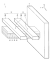
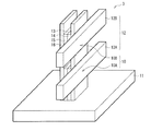
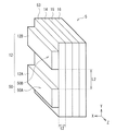
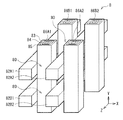
図1は、本開示の第1の実施の形態に係る記憶装置(メモリセルアレイ1)の構成を模式的に表したものである。このメモリセルアレイ1は、例えば図11に示した、所謂クロスポイント型の記憶装置(メモリセルアレイ6)の構成の一部であり、一の方向(例えばZ軸方向)に延伸する複数の第1の配線層(配線層12(12A,12B))と、他の方向(例えばY方向)に延伸する第2の配線層(配線層16)とが対向領域(即ち、配線層12と配線層16との交点)にそれぞれメモリセル10(10A,10B)が設けられたものである。本実施の形態では、メモリセル10は、例えば配線層12側から選択素子層13、中間電極層14および記憶素子層15がこの順に積層されており、これら各層13,14,15が配線層16と同一方向に延伸した構成を有する。<1. First Embodiment>
(1-1. Configuration of Storage Device)
FIG. 1 schematically illustrates a configuration of a storage device (memory cell array 1) according to the first embodiment of the present disclosure. This
配線層12(12A,12B)は、例えば基板11の平面(XZ平面)方向に対して略水平方向(例えば、Z軸方向)に延伸するものであり、例えば図6においてワード線(WL1,WL2)として用いられるものである。配線層16は、例えば基板11の平面(XZ平面)方向に対して略垂直方向(例えば、Y軸方向)に延伸するものであり、例えば図6においてピラー線(PL1)として用いられるものである。配線層12および配線層16は、半導体プロセスに用いられる配線材料、例えば、タングステン(W),窒化タングステン(WN),銅(Cu),アルミニウム(Al),モリブデン(Mo),タンタル(Ta)およびシリサイド等により構成されている。配線層12,16が選択素子層13または記憶素子層15との電界においてイオン伝導が生じる可能性のある材料(例えばCu)により構成されている場合には、Cuよりなる配線層12,16の表面を、W,WN,窒化チタン(TiN),TaN等のイオン伝導や熱拡散しにくい材料で被覆するようにしてもよい。なお、基板11には、CMOS回路や外部回路と連結するための回路(いずれも図示せず)等が設けられており、配線層12,16は、これらに接続されていてもよい。
The wiring layer 12 (12A, 12B) extends, for example, in a substantially horizontal direction (for example, the Z-axis direction) with respect to the plane (XZ plane) direction of the
選択素子層13は、印加電圧の増加とともに抵抗が大幅に低下し、印加電圧が低い場合に高抵抗状態を呈するものである。換言すると、選択素子層13は、印加電圧が低い場合には電気抵抗が高く、印加電圧が高い場合には電気抵抗が大幅に低下し、大電流(例えば数桁倍の電流)が流れる非線形の電気抵抗特性を有するものである。選択素子層13は、例えば、MSM(Metal-Semiconductor-Metal)ダイオード、MIM(Metal-Insulator-Metal)ダイオード、バリスタ、オボニック閾値スイッチを用いた構成としてもよく、複数の層から構成されていてもよい。また、選択素子層13は、記憶素子層15の動作方法によっては、単方向ダイオードまたは双方向ダイオードを用いてもよい。なお、選択素子層13は、例えば電圧印加によるイオンの移動によって形成される導電パスが印加電圧消去後にも維持される等のメモリ動作をしないものとする。
The resistance of the
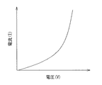
中間電極層14は、非線形特性を有するものであり、例えば、図2に示したように、電圧(V)の増加に対して電流(I)が指数関数的に増大する関係にある材料(非線形抵抗材料)によって形成されていることが好ましい。これにより、メモリセル10の選択特性が向上する。また、中間電極層14の電気抵抗によりメモリセル10の動作時に発生する瞬時電流を低減し、記憶素子層15への過度な電流を抑制することができる。更に、中間電極層14は、選択素子層13および記憶素子層15を構成する材料の相互拡散を抑制するためのものである。中間電極層14を構成する材料としては、例えば、窒素を含有する半導体材料を用いることが望ましい。具体的には、SiN、AlN、SiAlN、SiTiN、SiTaN、SiHfN、AlTiN、AlTaN、AlHfN等が挙げられる。これら窒化物半導体材料の窒素含有量を調整することにより、所望の特性を得ることができる。この他、中間電極層14は、ゲルマニウム(Ge)、酸素(O)、カルコゲナイド元素(例えば、硫黄(S)、セレン(Se)、テルル(Te))等を含有していてもよい。なお、中間電極層14は、選択素子層13および記憶素子層15と反応しやすい元素を含まないことが好ましい。例えば、選択素子層13および記憶素子層15を構成する主成分元素以外の元素を含んで構成されていることが好ましい。これにより、選択素子層13と記憶素子層15との間における上記元素の相互拡散が抑制される。
The
記憶素子層15は、電気的信号によって抵抗値が可逆的に変化するものであり、その変化した状態を保持することが可能な不揮発性を有する抵抗変化型のメモリ素子である。抵抗変化の原理は、相変化、分極、磁化方向および導電パス(フィラメント)の形成等、特に限定されるものではない。即ち、記憶素子層15は、例えば、PCM(相変化型メモリ素子)、FeRAM(強誘電体メモリ素子)、MRAM(磁気抵抗変化型メモリ素子)および遷移金属酸化物または、カルコゲナイドを含む抵抗変化メモリ素子のいずれを用いても構わない。
The
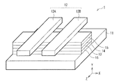
なお、図1では、選択素子層13、中間電極層14、記憶素子層15および配線層16が基板11に対して垂直方向に延伸している例を示したがこれに限らない。例えば、図3に示したように、選択素子層13、中間電極層14、記憶素子層15および配線層16が基板11に対して略水平方向(例えば、X軸方向)に延伸していてもよい。また、選択素子層13と記憶素子層15との位置を入れ替えてもよい。即ち、配線層12側から、記憶素子層15、中間電極層14および選択素子層13の順に積層された構成としてもよい。更に、図示していないが、配線層12および配線層16の上面あるいは、配線層12,16、選択素子層13、中間電極層14および記憶素子層15の各層の間には、他の層を形成しても構わない。他の層としては、例えば、密着性、平坦性および熱伝導性の改善あるいは、各層間における材料拡散の防止等を意図する層が形成される。
Although FIG. 1 shows an example in which the
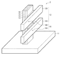
また、図1では、選択素子層13、中間電極層14および記憶素子層15の全てが配線層16と同一方向に延伸している例を示したがこれに限らない。例えば、図4に示したように、選択素子層13が、メモリセル10A,10Bごとに個別に形成されていても構わない。あるいは、図5に示したように、選択素子層13は共通層として形成され、中間電極層14および記憶素子層15がメモリセル10A,10Bごとに個別に形成されていても構わない。メモリセル10を構成する選択素子層13、中間電極層14および記憶素子層15のうちの少なくとも1層を共通層として形成することで、メモリセルを構成する各層をメモリセルごとに個別に形成する場合と比較して、製造工程を簡易にすることが可能となる。
FIG. 1 shows an example in which all of the
(1−2.記憶装置の動作)
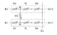
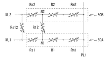
以下に、メモリセルアレイ1の動作について説明すると共に、本実施の形態の中間電極層14による効果について説明する。図6は、メモリセルアレイ1の等価回路図を簡易的に表したものである。図6では、配線層12Aと配線層16の交点における選択素子層13の抵抗をRs1、中間電極層14の抵抗をR1、記憶素子層15の抵抗をRm1とし、配線層12Bと配線層16の交点における選択素子層13の抵抗をRs2、中間電極層14の抵抗をR2、記憶素子層15の抵抗をRm2として表している。また、配線層12Aをワード線WL1、配線層12Bをワード線WL2、配線層16をピラー線PL1とし、Rs1とR1との接点をN1、Rs2とR2との接点をN2とする。また、メモリセル10Aをcell1、メモリセル10Bをcell2とする。(1-2. Operation of Storage Device)
Hereinafter, the operation of the
メモリセル10A(cell1)に書き込む場合を例に説明する。初期状態では、Rm1およびRm2は、共に高抵抗状態(Rm1H、Rm2H)にある。Rm1の書き込み閾値電圧Vthを、例えば3Vとする。メモリセル10A(cell1)への書き込み時には、ワード線WL1には書き込み電圧Vset1が印加され、ピラー線PL1はグランドに接続される。ワード線WL2にはVset1/2の電圧が印加される。上記の電圧設定では、Rs2はオン状態へは遷移せず高抵抗状態(オフ状態)のままであり、Rs1のみオン状態となって低抵抗状態へと遷移する。
A case where data is written to the
選択素子層13として、例えば、オボニック閾値スイッチを用いた場合を考える。Rs1がオン状態となった場合、Rs1の両端には所謂Holding Voltage Vholdが発生する。このため、R1およびRm1Hに印加される電圧は、V1=Vset1−Vholdとなる。このとき、R1<Rm1Hと設定されていることにより、V1は、ほぼRm1Hに印加され、Rm1Hの書き込み閾値電圧Vthよりも高くなる。低抵抗に遷移した後のRm1の抵抗値をRm1=RM1Lとすると、V1=(R1+RM1L)=×I1により定められる書き込み電流I1がRm1を流れることになる。
For example, consider a case where an ovonic threshold switch is used as the
記憶素子層15として、RRAMまたはPCMを用いた場合には、一般的に、RM1L×I1は、凡そ、一定値のVcell1となる。従って、I1=(V1−Vcell1)/R1とする。ここで、Rm1として十分な長期保存信頼性を確保するためには、I1が大きいことが望ましく、R1は低いほど有利となる。例えば、V1=5V、Vcell1=1Vとした場合、信頼性を確保するためには、例えば電流I1を40μAとすると、R1には4Vの電圧が印加されることになり、R1<100kΩが目安となる。
When RRAM or PCM is used as the
ところで、メモリセル10Aに書き込みするときには、メモリセル10Bに書き込みされてはいけない。図6において、メモリセル10A(cell1)とメモリセル10B(cell2)との間で異なる点はR12である。R12を十分高抵抗とすることによって、Rm2に印可される電圧は書き込み閾値電圧Vthより低くなるように設定される。高抵抗状態にあるRm2をRm2=Rm2Hとすると、R2<<Rm2Hなので、Rm2に印加される電圧VRm2Hは、VRm2H=V1×Rm2H/(R12+Rm2H)となる。一般的にRRAMおよびPCMにおける高抵抗状態の抵抗値は1MΩ以上である。VRm2Hが高くならないためには、R12は1MΩと同程度が望ましい。仮に、Rm2=R12=1MΩとした場合、R12とRm2には、V1/2の電圧が印加されることになる。例えば、V1=5Vの場合、V1/2=2.5Vとなり、メモリセル10Bには書き込みされない。従って、中間電極層14の電気抵抗R1は、例えば印加電圧が4Vのときには100kΩ以下であることが好ましく、例えば印加電圧2.5Vのときには1MkΩ以上であることが好ましい。即ち、電圧−電流特性が非線形性を有すること求められる。
By the way, when writing to the
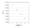
図7は、本実施の形態の中間電極層14を備えたメモリセルアレイ1における非線形特性を表したものである。図7では、印加電圧の増加とともに、抵抗値が減少しており、非線形特性となっている。なお、この結果は、中間電極層14を膜厚10nmのSiリッチのSiN膜として形成した場合のものである。
FIG. 7 shows non-linear characteristics in the
(1−3.作用・効果)
前述したように、メモリやストレージの大容量化および高速化を実現する手段として、メモリ素子と選択素子とを組み合わせたクロスポイント型メモリが提案されている。クロスポイント型メモリは、一の方向および他の方向に延伸する複数の配線層をそれぞれ有し、それらが互いに交差する配線間に、メモリ素子と選択素子とが直列に接続されたメモリセルが配置された構成を有する。このため、1つの配線層は複数のメモリセルによって共有されている。(1-3. Action / Effect)
As described above, a cross-point memory in which a memory element and a selection element are combined has been proposed as a means for increasing the capacity and speed of a memory or storage. The cross-point type memory has a plurality of wiring layers extending in one direction and the other direction, and a memory cell in which a memory element and a selection element are connected in series is arranged between wirings crossing each other. It has the structure which was done. Therefore, one wiring layer is shared by a plurality of memory cells.
クロスポイント型メモリのさらなる大容量化を実現する方法としては、例えば、平面に形成されたクロスポイント型メモリを積層していくことが考えられるが、クロスポイント型メモリの積層は製造コストの観点から限界があると言われている。そのため、将来的には、交差する2種類の配線層の一方を平面に対して垂直方向に延伸させ、メモリセルを垂直方向に形成する3次元立体構造を有するメモリの開発が有力視されている。 As a method of realizing a further increase in the capacity of the cross-point memory, for example, stacking cross-point memories formed on a plane can be considered. It is said that there is a limit. Therefore, in the future, development of a memory having a three-dimensional structure in which one of two kinds of intersecting wiring layers is extended in a direction perpendicular to a plane and a memory cell is formed in a vertical direction is considered to be promising. .
この3次元立体構造を有するメモリでは、例えば、基板に対して水平方向に延伸する複数の配線層が垂直方向に積層され、その配線間を、例えば基板に対して垂直方向に貫通する開孔が形成され、その開孔内にメモリセル構造体が設けられた構造が考えられている。メモリセル構造体では、開孔の側壁にメモリセルを構成する各層が順に成膜され、同心状の積層構造を形成している。このようなメモリセル構造体では、各層の膜厚は薄いことが好ましい。前述した3次元メモリアレイアーキテクチャでは、メモリセル構造体を構成する記憶素子材料およびセル選択材料は連続で成膜され、メモリセル構造体は複数の階層に渡って共有されるようになっている。 In the memory having the three-dimensional structure, for example, a plurality of wiring layers extending in the horizontal direction with respect to the substrate are vertically stacked, and an opening penetrating between the wirings, for example, in a direction perpendicular to the substrate. A structure in which a memory cell structure is formed and an opening is provided in the opening has been considered. In the memory cell structure, each layer constituting the memory cell is sequentially formed on the side wall of the opening to form a concentric laminated structure. In such a memory cell structure, the thickness of each layer is preferably small. In the above-described three-dimensional memory array architecture, the storage element material and the cell selection material constituting the memory cell structure are continuously formed, and the memory cell structure is shared over a plurality of levels.
しかしながら、クロスポイント型メモリは、上述したように、複数のメモリセルが1つの配線層を共有しているため、1つのメモリセルを選択して動作させる際に、選択したメモリセル(選択セル)以外の、配線層を共有しているその他のメモリセル(非選択セル)にも電圧が印加され、誤動作する虞がある。 However, in the cross-point type memory, as described above, since a plurality of memory cells share one wiring layer, when one memory cell is selected and operated, a selected memory cell (selected cell) is used. In addition, a voltage may be applied to other memory cells (non-selected cells) sharing a wiring layer, which may cause a malfunction.
また、メモリセルの特性を確保するためには、選択素子とメモリ素子との相互干渉による劣化を防ぐことが重要であり、その方法としては、選択素子とメモリ素子との間に、中間電極層を設けることが考えられている。前述した抵抗変化型メモリセルアレイでは、抵抗可変膜(メモリ素子)、導電層(中間電極層)、整流絶縁膜(選択素子)を設けることで、選択素子とメモリ素子との相互干渉を押さえ、メモリセルの特性の確保しつつ、劣化を抑制している。しかしながら、一般的な中間電極層では、隣り合うメモリセル間における電気的な短絡不良の発生が懸念される。隣り合うメモリセル間における電気的な短絡不良の発生は、非選択セルの誤動作に繋がる。以上のことから、クロスポイント型メモリでは、選択特性を向上させることが求められている。 Further, in order to ensure the characteristics of the memory cell, it is important to prevent deterioration due to mutual interference between the selection element and the memory element. As a method, an intermediate electrode layer is interposed between the selection element and the memory element. It is considered to provide. In the above-described variable resistance memory cell array, by providing a resistance variable film (memory element), a conductive layer (intermediate electrode layer), and a rectifying insulating film (selection element), mutual interference between the selection element and the memory element is suppressed, and Deterioration is suppressed while ensuring cell characteristics. However, in a general intermediate electrode layer, there is a concern that an electrical short circuit may occur between adjacent memory cells. The occurrence of an electrical short-circuit failure between adjacent memory cells leads to malfunction of unselected cells. From the above, in the cross-point type memory, it is required to improve the selection characteristics.
これに対して、本実施の形態のメモリセル10では、例えば配線層12側から選択素子層13、中間電極層14および記憶素子層15がこの順に積層されており、これら各層13,14,15が配線層16と同一方向に延伸した構成を有する。即ち、これら各層13,14,15はY軸方向に延伸する連続膜として形成されており、Y軸方向に並ぶメモリセル10Aおよびメモリセル10Bにおける共通層としてなっている。本実施の形態では、非線形抵抗材料を用いて中間電極層14を形成するようにした。これにより、隣接するメモリセル10Aとメモリセル10Bとの間における電気的短絡の発生を低減することが可能となる。
On the other hand, in the
以上のことから、本実施の形態のメモリセルアレイ1では、互いに交差する配線層12と配線層16との交点に設けられるメモリセル10を、中間電極層14を間に選択素子層13と記憶素子層15とが積層された構成とし、この中間電極層14を、非線形抵抗材料を用いて形成するようにした。これにより、隣接するメモリセル10Aおよびメモリセル10B間における電気的短絡の発生が低減される。よって、選択特性を向上させることが可能となる。
As described above, in the
ところで、選択素子と記憶素子との間に設けられた中間電極層による隣接セルへの電気的な短絡不良を防ぐ方法としては、中間電極層をセルごとに分断する、あるいは、酸化等により、中間電極層に高抵抗な領域を部分的に形成して隣接セル間を絶縁状態にする等が考えられる。しかしながら、その分製造工程が増えるという問題がある。 By the way, as a method of preventing an electric short circuit failure to an adjacent cell by an intermediate electrode layer provided between a selection element and a storage element, the intermediate electrode layer is divided for each cell, or the intermediate electrode layer is oxidized or the like. It is conceivable to partially form a high-resistance region in the electrode layer to make the adjacent cells insulated. However, there is a problem that the number of manufacturing steps increases accordingly.
これに対して、本実施の形態では、選択素子層13、中間電極層14および記憶素子層15を配線層16と共に、Y軸方向に延伸する連続膜として形成するようにしたので、メモリセルを構成する各層をメモリセルごとに個別に形成する場合と比較して、メモリセルアレイ1の製造工程を簡略化することが可能となる。即ち、本実施の形態のように、配線層12と配線層16との対向領域に形成されるメモリセル10を、非線形抵抗材料を含む中間電極層14を間に選択素子層13と記憶素子層15とが積層された構成とし、さらに、選択素子層13、中間電極層14および記憶素子層15が、例えば配線層16と同一方向に延伸する連続膜として形成することで、製造工程の容易性と、高い選択性とを両立することが可能となる。
On the other hand, in the present embodiment, the
次に、第2および第3の実施の形態ならびに変形例について説明する。以下では、上記第1の実施の形態と同様の構成要素については同一の符号を付し、適宜その説明を省略する。 Next, second and third embodiments and modified examples will be described. In the following, the same components as those in the first embodiment are denoted by the same reference numerals, and description thereof will be omitted as appropriate.
<2.第2の実施の形態>
図8は、本開示の第2の実施の形態に係る記憶装置(メモリセルアレイ4)の構成を模式的に表したものである。このメモリセルアレイ4は、上記第1の実施の形態におけるメモリセルアレイ1等と同様に、例えば、図11に示した、所謂クロスポイント型の記憶装置(メモリセルアレイ6)の構成の一部であり、一の方向(例えばZ軸方向)に延伸する複数の第1の配線層(配線層12(12A,12B))と、他の方向(例えばY方向)に延伸する第2の配線層(配線層16)とが交差する対向領域にそれぞれメモリセル40(40A,40B)が設けられたものである。本実施の形態では、配線層12Aと配線層16との対向領域に設けられたメモリセル40における中間電極層44の膜厚方向(X軸方向)の電気抵抗(例えば、メモリセル40Aにおける電気抵抗R1)が、隣接する非対向領域(例えば、メモリセル40Aとメモリセル40Bとの間)における中間電極層44の電気抵抗R12よりも低い構成を有する。<2. Second Embodiment>
FIG. 8 schematically illustrates a configuration of a storage device (memory cell array 4) according to the second embodiment of the present disclosure. This
中間電極層44は、上記中間電極層24と同様に、非線形特性を有するものであると共に、選択素子層13および記憶素子層15を構成する材料の相互拡散を抑制するためのものである。中間電極層44を構成する材料としては、非線形抵抗材料を用いることが好ましく、例えば、窒素を含有する半導体材料を用いることが望ましい。具体的には、SiN、AlN、SiAlN、SiTiN、SiTaN、SiHfN、AlTiN、AlTaN、AlHfN等が挙げられる。これら窒化物半導体材料の窒素含有量を調整することにより、所望の特性を得ることができる。この他、中間電極層44は、ゲルマニウム(Ge)、酸素(O)、カルコゲナイド元素(例えば、硫黄(S)、セレン(Se)、テルル(Te))等を含有していてもよい。なお、中間電極層44は、選択素子層13および記憶素子層15と反応しやすい元素を含まないことが好ましく、これにより、相互拡散を抑制することができる。
The
メモリセル40Aにおける中間電極層44の膜厚方向の電気抵抗R1を低く、隣接するメモリセル40Aとメモリセル40Bとの間の中間電極層44の電気抵抗R12を高くする方法としては、中間電極層44の膜厚t1を、隣り合うメモリセル40Aとメモリセル40B間の距離L1よりも小さくすることが好ましい。これにより、中間電極層44の電気抵抗R1を相対的に低くすることができる。換言すると、配線層12Aと配線層12Bとの距離を大きくすることにより、中間電極層44の電気抵抗R12を高くすることができる。この場合、メモリセルアレイにおける面積効率は犠牲となるが、安定性は向上する。あるいは、中間電極層44の一部を意図的に酸化または、損傷を与えることにより、中間電極層44の抵抗を高くすることができる。この他、例えば中間電極層44を積層構造とし、材料抵抗に異方性を持たせることで、電気抵抗R1を相対的に低くすることができる。
As a method for lowering the electric resistance R1 of the
上記第1の実施の形態と同様に、メモリセルアレイにおいて隣接するメモリセルへの誤書き込みを抑制する構成としては、中間電極層44の電気抵抗が、膜厚方向(X軸方向)の電気抵抗R1がより低く、延伸方向(Y軸方向)の電気抵抗R12がより高いことが好ましい。本実施の形態では、例えばメモリセル40Aにおける中間電極層44の膜厚方向の電気抵抗R1を低く、隣接するメモリセル40Aとメモリセル40Bとの間の中間電極層44の電気抵抗R12を高くするようにしたので、誤書き込みの発生を抑制し、選択特性をさらに向上させることが可能となる。
As in the first embodiment, as a configuration for suppressing erroneous writing to an adjacent memory cell in the memory cell array, the electric resistance of the
<3.第3の実施の形態>
図9は、本開示の第3の実施の形態に係る記憶装置(メモリセルアレイ5)の構成を模式的に表したものである。このメモリセルアレイ5は、上記第1の実施の形態におけるメモリセルアレイ1等と同様に、例えば、図11に示した、所謂クロスポイント型の記憶装置(メモリセルアレイ6)の構成の一部であり、一の方向(例えばZ軸方向)に延伸する複数の第1の配線層(配線層12(12A,12B))と、他の方向(例えばY方向)に延伸する第2の配線層(配線層16)とが交差する対向領域にそれぞれメモリセル50(50A,50B)が設けられたものである。本実施の形態では、配線層12Aと配線層16との対向領域に設けられたメモリセル50(例えば、メモリセル50A)における選択素子層53の膜厚方向(X軸方向)の電気抵抗Rs1が、隣接する非対向領域(例えば、メモリセル50Aとメモリセル50Bとの間)における選択素子層53の電気抵抗Rs12よりも低い構成を有する。<3. Third Embodiment>
FIG. 9 schematically illustrates a configuration of a storage device (memory cell array 5) according to the third embodiment of the present disclosure. The
選択素子層53は、印加電圧の増加とともに抵抗が大幅に低下し、印加電圧が低い場合に高抵抗状態を呈するものである。選択素子層53は、例えば、MSMダイオード、MIMダイオード、バリスタ、オボニック閾値スイッチを用いて構成されていてもよく、複数の層から構成されていてもよい。また、選択素子層53は、記憶素子層15の動作方法によっては、単方向ダイオードまたは双方向ダイオードを用いてもよい。なお、選択素子層53は、例えば電圧印加によるイオンの移動によって形成される導電パスが印加電圧消去後にも維持される等のメモリ動作をしないものとする。
The resistance of the
上記第1の実施の形態等では、メモリセルアレイにおいて隣接するメモリセルへの誤書き込みを抑制する構成として、延伸方向の中間電極層14の電気抵抗R12が膜厚方向の電気抵抗R1よりも高いとすることが好ましいとしたが、延伸方向の電気抵抗という観点では、選択素子層13においても同様のことが言える。
In the first embodiment and the like, as a configuration for suppressing erroneous writing to an adjacent memory cell in the memory cell array, the electric resistance R12 of the
図10は、本実施の形態のメモリセルアレイ5の等価回路を表したものである。選択素子層53の延伸方向(Y軸方向)の電気抵抗Rs12が極端に低い場合、選択素子層53は選択素子として機能せずに誤動作の原因となる。よって、選択素子層53の積層方向(X軸方向)の膜厚t2は、隣接する隣り合うメモリセル50Aとメモリセル50B間の距離L2よりも小さくすることが好ましい。これにより、選択素子層53の電気抵抗Rs1を相対的に低くすることができる。換言すると、配線層12Aと配線層12Bとの距離を大きくすることにより、選択素子層53の電気抵抗Rs12を高くすることができる。
FIG. 10 illustrates an equivalent circuit of the
以上のように、本実施の形態では、例えばメモリセル50Aにおける選択素子層53の膜厚方向の電気抵抗R1を低く、隣接するメモリセル50Aとメモリセル50Bとの間の選択素子層53の電気抵抗R12を高くするようにしたので、誤書き込みの発生を抑制し、選択特性をさらに向上させることが可能となる。
As described above, in the present embodiment, for example, the electric resistance R1 in the thickness direction of the
なお、本実施の形態では、選択素子層53は隣り合うメモリセル50Aおよびメモリセル50Bとの間で連続する連続膜として形成されている必要があるが、中間電極層14および記憶素子層15はメモリセル50Aおよびメモリセル50Bごとに、個別に形成されていても構わない。その場合には、中間電極層14は、必ずしも非線形特性を有していなくてもよい。但し、非線形特性を有する材料を用いて中間電極層14を形成することにより、上述したように、メモリセル50Aの選択特性が向上すると共に、中間電極層14の電気抵抗によりメモリセル50Aの動作時に発生する瞬時電流が低減され、記憶素子層15への過度な電流が抑制される。
In this embodiment, the
<4.変形例>
(変形例1)
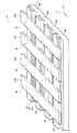
図11は、本開示の変形例1に係る記憶装置(メモリセルアレイ6)の構成の一例を模式的に表したものである。このメモリセルアレイ6は、例えば、図3に示したメモリセルアレイ1を拡張したものであり、複数の配線層62(62A,62B,62C,62D)および複数の配線層66(66A,66B,66C,66D)を有し、各配線層66A,66B,66C,66Dに沿って、選択素子層63、中間電極層64および記憶素子層65が連続膜として形成されたものである。このメモリセルアレイ6では、選択素子層63、中間電極層64および記憶素子層65は、各配線層62A,62B,62C,62Dによって共有されている。即ち、メモリセルアレイ6は、例えばZ軸方向に延伸する複数の配線層62(62A,62B,62C,62D)と、例えばZ軸方向に延伸する複数の配線層66(66A,66B,66C,66D)とが互いに対向する位置(クロスポイント)にそれぞれメモリセル10を有するクロスポイント型のメモリセルアレイであり、本開示の記憶装置の一具体例に相当するものである。<4. Modification>
(Modification 1)
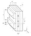
FIG. 11 schematically illustrates an example of a configuration of a storage device (memory cell array 6) according to the first modification of the present disclosure. The
(変形例2)
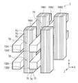
図12は、本開示の変形例2に係る記憶装置(メモリセルアレイ7)の構成を模式的に表したものである。このメモリセルアレイ7は、例えば、Z軸方向に延伸する複数の配線層72(配線層72A1と配線層72A2、配線層72B1と配線層72B2)およびY軸方向に延伸する複数の配線層76(配線層76A1と配線層76A2、配線層76B1と配線層76B2)が、それぞれX軸方向に積層された3次元構造を有するものである。このメモリセルアレイ7では、配線層76の両側に、記憶素子層75、中間電極層74および選択素子層73がこの順に積層された構成となっている。(Modification 2)
FIG. 12 schematically illustrates a configuration of a storage device (memory cell array 7) according to
(変形例3)
図13は、本開示の変形例3に係る記憶装置(メモリセルアレイ8)の構成を模式的に表したものである。このメモリセルアレイ8は、例えば、上記変形例2におけるメモリセルアレイ7と同様に、Z軸方向に延伸する複数の配線層82(配線層82A1と配線層82A2、配線層82B1と配線層82B2)およびY軸方向に延伸する複数の配線層86(配線層86A1と配線層86A2、配線層86B1と配線層86B2)が、それぞれX軸方向に積層された3次元構造を有するものである。このメモリセルアレイ8では、配線層86の側面全体が記憶素子層85、中間電極層84および選択素子層83の順に覆われた構成となっている。即ち、配線層86を中心に、中間電極層84および選択素子層83がこの順に同心状に積層された構成を有する。(Modification 3)
FIG. 13 schematically illustrates a configuration of a storage device (memory cell array 8) according to
以上のように、変形例2,3に示したメモリセルアレイ7,8は、複数のメモリセルを平面(2次元,例えば、YZ平面方向)に配置し、さらにX軸方向に積層させた3次元構造としたものであり、このように3次元構造とすることで、より高密度且つ大容量な記憶装置を提供することができる。
As described above, the
以上、第1〜第3の実施の形態およびその変形例(変形例1〜3)を挙げて本開示を説明したが、本開示内容は上記実施の形態等に限定されるものではなく、種々変形が可能である。例えば、図示していないが、例えば、図1の配線層12A,12Bの間の空隙や図12における各配線層12,16の間の空隙には、絶縁膜が形成されていてもよい。 As described above, the present disclosure has been described with reference to the first to third embodiments and modified examples (modified examples 1 to 3). However, the content of the present disclosure is not limited to the above-described embodiments and the like. Deformation is possible. For example, although not shown, for example, an insulating film may be formed in a gap between the wiring layers 12A and 12B in FIG. 1 and a gap between the wiring layers 12 and 16 in FIG.
また、本変形例2,3では、例えば配線層12,16の断面形状を矩形形状で示したがこれに限定されるものではない。例えば、Y軸方向に延伸する配線層86の断面形状は、円形状、楕円形状等の他の形状で形成されていてもよい。また、本開示の記憶装置は、上記第1〜第3の実施の形態および変形例1〜3を各々組み合わせた構造としてもよい。
In the second and third modifications, for example, the cross-sectional shape of the wiring layers 12 and 16 is shown as a rectangular shape, but is not limited to this. For example, the cross-sectional shape of the wiring layer 86 extending in the Y-axis direction may be formed in another shape such as a circular shape or an elliptical shape. Further, the storage device of the present disclosure may have a structure in which the first to third embodiments and
なお、本明細書中に記載された効果は、あくまで例示であり、本開示の効果は、本明細書中に記載された効果に限定されるものではない。また、本開示内容が、本明細書中に記載された効果以外の効果を持っていてもよい。 Note that the effects described in this specification are merely examples, and the effects of the present disclosure are not limited to the effects described in this specification. Further, the present disclosure may have effects other than the effects described in the present specification.
また、例えば、本開示は以下のような構成を取ることができる。
(1)
一の方向に延伸する複数の第1の配線層と、
他の方向に延伸する複数の第2の配線層と、
前記複数の第1の配線層と前記複数の第2の配線層との対向領域にそれぞれ設けられた複数のメモリセルとを備え、
前記複数のメモリセルはそれぞれ、選択素子層と、記憶素子層と、前記選択素子層と前記記憶素子層との間に設けられた中間電極層とを有し、
前記選択素子層、前記記憶素子層および前記中間電極層のうちの少なくとも1つは、前記一の方向または前記他の方向に延伸して隣り合う前記複数のメモリセル間における共通層となっており、
前記中間電極層は、非線形抵抗材料を含んで形成されている
記憶装置。
(2)
前記中間電極層が前記共通層として形成されている、前記(1)に記載の記憶装置。
(3)
前記選択素子層が前記共通層として形成されている、前記(1)に記載の記憶装置。
(4)
前記記憶素子層が前記共通層として形成されている、前記(1)に記載の記憶装置。
(5)
前記中間電極層および前記選択素子層は、それぞれ、前記一の方向または前記他の方向に延伸している、前記(1)に記載の記憶装置。
(6)
前記中間電極層および前記記憶素子層は、それぞれ、前記一の方向または前記他の方向に延伸している、前記(1)に記載の記憶装置。
(7)
前記選択素子層および前記記憶素子層は、それぞれ、前記一の方向または前記他の方向に延伸している、前記(1)に記載の記憶装置。
(8)
前記選択素子層、前記記憶素子層および前記中間電極層は、それぞれ、前記一の方向または前記他の方向に延伸している、前記(1)に記載の記憶装置。
(9)
前記選択素子層、前記記憶素子層および前記中間電極層のうちの少なくとも2つが同一方向に延伸している、前記(1)乃至(7)のうちのいずれかに記載の記憶装置。
(10)
前記選択素子層、前記記憶素子層および前記中間電極層は同一方向に延伸している、前記(1)乃至(8)のうちのいずれかに記載の記憶装置。
(11)
前記複数の第1の配線層、前記複数の第2の配線層および前記複数のメモリセルは基板上に配設され、
前記複数の第1の配線層および前記複数の第2の配線層は、前記基板に対して略水平方向に延伸している、前記(1)乃至(10)のうちのいずれかに記載の記憶装置。
(12)
前記複数の第1の配線層、前記複数の第2の配線層および前記複数のメモリセルは基板上に配設され、
前記複数の第1の配線層および前記複数の第2の配線層の一方は、前記基板に対して略垂直方向に延伸している、前記(1)乃至(10)のうちのいずれかに記載の記憶装置。
(13)
前記中間電極層の前記対向領域における膜厚方向の電気抵抗は、隣り合う前記複数の第1の配線層の間の非対向領域における電気抵抗よりも低い、前記(1)乃至(12)のうちのいずれかに記載の記憶装置。
(14)
前記選択素子層の膜厚は、隣り合う前記複数の第1の配線層の間の距離よりも小さい、前記(1)乃至(13)のうちのいずれかに記載の記憶装置。
(15)
前記中間電極層は、前記選択素子層および前記記憶素子層を構成する主成分元素以外の元素を含んで構成されている、前記(1)乃至(14)のうちのいずれかに記載の記憶装置。
(16)
前記選択素子層は、印加電圧の増加とともに抵抗が大幅に低下し、印加電圧が低い場合に高抵抗状態を呈する、前記(1)乃至(15)のうちのいずれかに記載の記憶装置。
(17)
前記記憶素子層は、相変化型メモリ素子、強誘電体メモリ素子、遷移金属酸化物または、カルコゲナイドを含む抵抗変化メモリ素子および磁気抵抗変化型メモリ素子のいずれかである、前記(1)乃至(16)のうちのいずれかに記載の記憶装置。Further, for example, the present disclosure can have the following configurations.
(1)
A plurality of first wiring layers extending in one direction;
A plurality of second wiring layers extending in other directions;
A plurality of memory cells provided in regions facing the plurality of first wiring layers and the plurality of second wiring layers, respectively;
Each of the plurality of memory cells includes a selection element layer, a storage element layer, and an intermediate electrode layer provided between the selection element layer and the storage element layer,
At least one of the selection element layer, the storage element layer, and the intermediate electrode layer is a common layer between the plurality of adjacent memory cells extending in the one direction or the other direction. ,
The storage device, wherein the intermediate electrode layer is formed including a non-linear resistance material.
(2)
The storage device according to (1), wherein the intermediate electrode layer is formed as the common layer.
(3)
The storage device according to (1), wherein the selection element layer is formed as the common layer.
(4)
The storage device according to (1), wherein the storage element layer is formed as the common layer.
(5)
The storage device according to (1), wherein the intermediate electrode layer and the selection element layer extend in the one direction or the other direction, respectively.
(6)
The storage device according to (1), wherein the intermediate electrode layer and the storage element layer extend in the one direction or the other direction, respectively.
(7)
The storage device according to (1), wherein the selection element layer and the storage element layer extend in the one direction or the other direction, respectively.
(8)
The storage device according to (1), wherein the selection element layer, the storage element layer, and the intermediate electrode layer extend in the one direction or the other direction, respectively.
(9)
The storage device according to any one of (1) to (7), wherein at least two of the selection element layer, the storage element layer, and the intermediate electrode layer extend in the same direction.
(10)
The storage device according to any one of (1) to (8), wherein the selection element layer, the storage element layer, and the intermediate electrode layer extend in the same direction.
(11)
The plurality of first wiring layers, the plurality of second wiring layers, and the plurality of memory cells are provided on a substrate,
The storage according to any one of (1) to (10), wherein the plurality of first wiring layers and the plurality of second wiring layers extend in a substantially horizontal direction with respect to the substrate. apparatus.
(12)
The plurality of first wiring layers, the plurality of second wiring layers, and the plurality of memory cells are provided on a substrate,
One of the above (1) to (10), wherein one of the plurality of first wiring layers and the plurality of second wiring layers extends in a direction substantially perpendicular to the substrate. Storage device.
(13)
In the above (1) to (12), the electric resistance in the thickness direction in the facing region of the intermediate electrode layer is lower than the electric resistance in the non-facing region between the plurality of adjacent first wiring layers. The storage device according to any one of the above.
(14)
The storage device according to any one of (1) to (13), wherein the thickness of the selection element layer is smaller than a distance between the plurality of adjacent first wiring layers.
(15)
The storage device according to any one of (1) to (14), wherein the intermediate electrode layer is configured to include an element other than a main component element constituting the selection element layer and the storage element layer. .
(16)
The memory device according to any one of (1) to (15), wherein the resistance of the selection element layer significantly decreases with an increase in applied voltage, and exhibits a high resistance state when the applied voltage is low.
(17)
The memory element layer is any of a phase-change memory element, a ferroelectric memory element, a resistance-change memory element containing a transition metal oxide or chalcogenide, and a magneto-resistance change-type memory element. A storage device according to any one of 16).
本出願は、日本国特許庁において2017年4月11日に出願された日本特許出願番号2017−078256号を基礎として優先権を主張するものであり、この出願の全ての内容を参照によって本出願に援用する。 This application claims priority based on Japanese Patent Application No. 2017-078256 filed on April 11, 2017 by the Japan Patent Office. The entire contents of this application are incorporated herein by reference. Invite to
当業者であれば、設計上の要件や他の要因に応じて、種々の修正、コンビネーション、サブコンビネーション、および変更を想到し得るが、それらは添付の請求の範囲やその均等物の範囲に含まれるものであることが理解される。 Various modifications, combinations, sub-combinations, and modifications may occur to those skilled in the art, depending on design requirements and other factors, which are within the scope of the appended claims and their equivalents. It is understood that it is.
Claims (17)
他の方向に延伸する複数の第2の配線層と、
前記複数の第1の配線層と前記複数の第2の配線層との対向領域にそれぞれ設けられた複数のメモリセルとを備え、
前記複数のメモリセルはそれぞれ、選択素子層と、記憶素子層と、前記選択素子層と前記記憶素子層との間に設けられた中間電極層とを有し、
前記選択素子層、前記記憶素子層および前記中間電極層のうちの少なくとも1つは、前記一の方向または前記他の方向に延伸して隣り合う前記複数のメモリセル間における共通層となっており、
前記中間電極層は、非線形抵抗材料を含んで形成されている
記憶装置。A plurality of first wiring layers extending in one direction;
A plurality of second wiring layers extending in other directions;
A plurality of memory cells provided in regions facing the plurality of first wiring layers and the plurality of second wiring layers, respectively;
Each of the plurality of memory cells includes a selection element layer, a storage element layer, and an intermediate electrode layer provided between the selection element layer and the storage element layer,
At least one of the selection element layer, the storage element layer, and the intermediate electrode layer is a common layer between the plurality of adjacent memory cells extending in the one direction or the other direction. ,
The storage device, wherein the intermediate electrode layer is formed including a non-linear resistance material.
前記複数の第1の配線層および前記複数の第2の配線層は、前記基板に対して略水平方向に延伸している、請求項1に記載の記憶装置。The plurality of first wiring layers, the plurality of second wiring layers, and the plurality of memory cells are provided on a substrate,
The storage device according to claim 1, wherein the plurality of first wiring layers and the plurality of second wiring layers extend in a substantially horizontal direction with respect to the substrate.
前記複数の第1の配線層および前記複数の第2の配線層の一方は、前記基板に対して略垂直方向に延伸している、請求項1に記載の記憶装置。The plurality of first wiring layers, the plurality of second wiring layers, and the plurality of memory cells are provided on a substrate,
The storage device according to claim 1, wherein one of the plurality of first wiring layers and the plurality of second wiring layers extends in a direction substantially perpendicular to the substrate.
Applications Claiming Priority (3)
| Application Number | Priority Date | Filing Date | Title |
|---|---|---|---|
| JP2017078256 | 2017-04-11 | ||
| JP2017078256 | 2017-04-11 | ||
| PCT/JP2018/010255 WO2018190071A1 (en) | 2017-04-11 | 2018-03-15 | Storage device |
Publications (1)
| Publication Number | Publication Date |
|---|---|
| JPWO2018190071A1 true JPWO2018190071A1 (en) | 2020-02-20 |
Family
ID=63792468
Family Applications (1)
| Application Number | Title | Priority Date | Filing Date |
|---|---|---|---|
| JP2019512395A Pending JPWO2018190071A1 (en) | 2017-04-11 | 2018-03-15 | Storage device |
Country Status (6)
| Country | Link |
|---|---|
| US (1) | US11018189B2 (en) |
| JP (1) | JPWO2018190071A1 (en) |
| KR (1) | KR102462182B1 (en) |
| CN (1) | CN110494972A (en) |
| TW (1) | TWI759457B (en) |
| WO (1) | WO2018190071A1 (en) |
Families Citing this family (5)
| Publication number | Priority date | Publication date | Assignee | Title |
|---|---|---|---|---|
| US10847578B1 (en) * | 2019-07-03 | 2020-11-24 | Windbond Electronics Corp. | Three-dimensional resistive memories and methods for forming the same |
| JP2021144771A (en) | 2020-03-12 | 2021-09-24 | キオクシア株式会社 | Semiconductor storage device and memory system |
| US11444126B2 (en) * | 2020-07-24 | 2022-09-13 | Taiwan Semiconductor Manufacturing Company, Ltd. | Memory device and manufacturing method thereof |
| JP7467278B2 (en) * | 2020-08-17 | 2024-04-15 | キオクシア株式会社 | Semiconductor memory device |
| KR20230168481A (en) * | 2022-06-07 | 2023-12-14 | 삼성전자주식회사 | Memory device and electronic device including the memory device |
Citations (5)
| Publication number | Priority date | Publication date | Assignee | Title |
|---|---|---|---|---|
| JP2011129639A (en) * | 2009-12-16 | 2011-06-30 | Toshiba Corp | Resistance change type memory cell array |
| WO2012001960A1 (en) * | 2010-07-01 | 2012-01-05 | パナソニック株式会社 | Nonvolatile memory cell, nonvolatile memory cell array, and method for manufacturing the nonvolatile memory cell array |
| WO2012169198A1 (en) * | 2011-06-10 | 2012-12-13 | パナソニック株式会社 | Nonvolatile storage element, method of manufacturing thereof, initial breaking method, and nonvolatile storage device |
| WO2014103577A1 (en) * | 2012-12-26 | 2014-07-03 | ソニー株式会社 | Storage apparatus and method for manufacturing same |
| WO2016129306A1 (en) * | 2015-02-10 | 2016-08-18 | ソニー株式会社 | Selective element, memory cell and storage device |
Family Cites Families (6)
| Publication number | Priority date | Publication date | Assignee | Title |
|---|---|---|---|---|
| US6870755B2 (en) * | 2002-08-02 | 2005-03-22 | Unity Semiconductor Corporation | Re-writable memory with non-linear memory element |
| WO2008149493A1 (en) * | 2007-06-01 | 2008-12-11 | Panasonic Corporation | Resistance change type memory |
| DE602008006652D1 (en) * | 2007-06-05 | 2011-06-16 | Panasonic Corp | NON-VOLATILE MEMORY ELEMENT, METHOD FOR THE PRODUCTION THEREOF, AND NON-VOLATILE SEMICONDUCTOR DEVICE WITH THE NON-VOLATILE MEMORY ELEMENT |
| JP2009004725A (en) * | 2007-09-25 | 2009-01-08 | Panasonic Corp | Variable resistance nonvolatile memory device |
| JP2010225741A (en) * | 2009-03-23 | 2010-10-07 | Toshiba Corp | Nonvolatile semiconductor memory device |
| US8729523B2 (en) * | 2012-08-31 | 2014-05-20 | Micron Technology, Inc. | Three dimensional memory array architecture |
-
2018
- 2018-03-15 WO PCT/JP2018/010255 patent/WO2018190071A1/en not_active Ceased
- 2018-03-15 KR KR1020197028412A patent/KR102462182B1/en active Active
- 2018-03-15 CN CN201880021327.3A patent/CN110494972A/en not_active Withdrawn
- 2018-03-15 JP JP2019512395A patent/JPWO2018190071A1/en active Pending
- 2018-03-15 US US16/490,303 patent/US11018189B2/en not_active Expired - Fee Related
- 2018-04-03 TW TW107111786A patent/TWI759457B/en not_active IP Right Cessation
Patent Citations (5)
| Publication number | Priority date | Publication date | Assignee | Title |
|---|---|---|---|---|
| JP2011129639A (en) * | 2009-12-16 | 2011-06-30 | Toshiba Corp | Resistance change type memory cell array |
| WO2012001960A1 (en) * | 2010-07-01 | 2012-01-05 | パナソニック株式会社 | Nonvolatile memory cell, nonvolatile memory cell array, and method for manufacturing the nonvolatile memory cell array |
| WO2012169198A1 (en) * | 2011-06-10 | 2012-12-13 | パナソニック株式会社 | Nonvolatile storage element, method of manufacturing thereof, initial breaking method, and nonvolatile storage device |
| WO2014103577A1 (en) * | 2012-12-26 | 2014-07-03 | ソニー株式会社 | Storage apparatus and method for manufacturing same |
| WO2016129306A1 (en) * | 2015-02-10 | 2016-08-18 | ソニー株式会社 | Selective element, memory cell and storage device |
Also Published As
| Publication number | Publication date |
|---|---|
| TW201843681A (en) | 2018-12-16 |
| WO2018190071A1 (en) | 2018-10-18 |
| US20200052040A1 (en) | 2020-02-13 |
| KR102462182B1 (en) | 2022-11-03 |
| CN110494972A (en) | 2019-11-22 |
| TWI759457B (en) | 2022-04-01 |
| US11018189B2 (en) | 2021-05-25 |
| KR20190137797A (en) | 2019-12-11 |
Similar Documents
| Publication | Publication Date | Title |
|---|---|---|
| JP6151650B2 (en) | Storage device | |
| US9059391B2 (en) | Self-rectifying RRAM cell structure and 3D crossbar array architecture thereof | |
| US7791060B2 (en) | Semiconductor memory device and method of controlling the same | |
| JP4538067B2 (en) | Semiconductor memory device | |
| KR102488896B1 (en) | switch element and memory | |
| US10056432B2 (en) | Self-rectifying RRAM cell structure having two resistive switching layers with different bandgaps and RRAM 3D crossbar array architecture | |
| KR20200126971A (en) | Switch elements and storage devices, and memory systems | |
| TWI759457B (en) | memory device | |
| JP6577954B2 (en) | Switching components and memory units | |
| JPWO2019198410A1 (en) | Switch elements and storage devices and memory systems | |
| JPWO2016052097A1 (en) | Switch element and storage device | |
| TWI733520B (en) | Memory cell, memory device and method of amplifying data using selector element of memory cell | |
| TW201719879A (en) | Self-aligned memory array | |
| JP2013197420A (en) | Resistance change memory element | |
| US20180211913A1 (en) | Cross-point array device including conductive fuse material layer | |
| KR102706417B1 (en) | Electronic device | |
| KR102706732B1 (en) | Electronic device and method for fabricating the same | |
| JP2011035202A (en) | Semiconductor memory device | |
| US10629653B2 (en) | Cross-point array device including conductive fuse material layer | |
| TW201828455A (en) | Structure of random access memory | |
| KR20240149637A (en) | Semiconductor device |
Legal Events
| Date | Code | Title | Description |
|---|---|---|---|
| A621 | Written request for application examination |
Free format text: JAPANESE INTERMEDIATE CODE: A621 Effective date: 20210202 |
|
| A131 | Notification of reasons for refusal |
Free format text: JAPANESE INTERMEDIATE CODE: A131 Effective date: 20211005 |
|
| A521 | Request for written amendment filed |
Free format text: JAPANESE INTERMEDIATE CODE: A523 Effective date: 20211129 |
|
| A02 | Decision of refusal |
Free format text: JAPANESE INTERMEDIATE CODE: A02 Effective date: 20220426 |