JPWO2018216632A1 - Piezoelectric sensor and method of manufacturing the same - Google Patents
Piezoelectric sensor and method of manufacturing the same Download PDFInfo
- Publication number
- JPWO2018216632A1 JPWO2018216632A1 JP2019520227A JP2019520227A JPWO2018216632A1 JP WO2018216632 A1 JPWO2018216632 A1 JP WO2018216632A1 JP 2019520227 A JP2019520227 A JP 2019520227A JP 2019520227 A JP2019520227 A JP 2019520227A JP WO2018216632 A1 JPWO2018216632 A1 JP WO2018216632A1
- Authority
- JP
- Japan
- Prior art keywords
- electrode
- piezoelectric body
- linear expansion
- piezoelectric
- expansion coefficient
- Prior art date
- Legal status (The legal status is an assumption and is not a legal conclusion. Google has not performed a legal analysis and makes no representation as to the accuracy of the status listed.)
- Granted
Links
Images


Classifications
-
- G—PHYSICS
- G01—MEASURING; TESTING
- G01L—MEASURING FORCE, STRESS, TORQUE, WORK, MECHANICAL POWER, MECHANICAL EFFICIENCY, OR FLUID PRESSURE
- G01L1/00—Measuring force or stress, in general
- G01L1/16—Measuring force or stress, in general using properties of piezoelectric devices
-
- G—PHYSICS
- G01—MEASURING; TESTING
- G01L—MEASURING FORCE, STRESS, TORQUE, WORK, MECHANICAL POWER, MECHANICAL EFFICIENCY, OR FLUID PRESSURE
- G01L9/00—Measuring steady of quasi-steady pressure of fluid or fluent solid material by electric or magnetic pressure-sensitive elements; Transmitting or indicating the displacement of mechanical pressure-sensitive elements, used to measure the steady or quasi-steady pressure of a fluid or fluent solid material, by electric or magnetic means
- G01L9/08—Measuring steady of quasi-steady pressure of fluid or fluent solid material by electric or magnetic pressure-sensitive elements; Transmitting or indicating the displacement of mechanical pressure-sensitive elements, used to measure the steady or quasi-steady pressure of a fluid or fluent solid material, by electric or magnetic means by making use of piezoelectric devices, i.e. electric circuits therefor
-
- H—ELECTRICITY
- H10—SEMICONDUCTOR DEVICES; ELECTRIC SOLID-STATE DEVICES NOT OTHERWISE PROVIDED FOR
- H10N—ELECTRIC SOLID-STATE DEVICES NOT OTHERWISE PROVIDED FOR
- H10N30/00—Piezoelectric or electrostrictive devices
- H10N30/01—Manufacture or treatment
- H10N30/06—Forming electrodes or interconnections, e.g. leads or terminals
- H10N30/067—Forming single-layered electrodes of multilayered piezoelectric or electrostrictive parts
-
- H—ELECTRICITY
- H10—SEMICONDUCTOR DEVICES; ELECTRIC SOLID-STATE DEVICES NOT OTHERWISE PROVIDED FOR
- H10N—ELECTRIC SOLID-STATE DEVICES NOT OTHERWISE PROVIDED FOR
- H10N30/00—Piezoelectric or electrostrictive devices
- H10N30/01—Manufacture or treatment
- H10N30/09—Forming piezoelectric or electrostrictive materials
- H10N30/093—Forming inorganic materials
- H10N30/097—Forming inorganic materials by sintering
-
- H—ELECTRICITY
- H10—SEMICONDUCTOR DEVICES; ELECTRIC SOLID-STATE DEVICES NOT OTHERWISE PROVIDED FOR
- H10N—ELECTRIC SOLID-STATE DEVICES NOT OTHERWISE PROVIDED FOR
- H10N30/00—Piezoelectric or electrostrictive devices
- H10N30/30—Piezoelectric or electrostrictive devices with mechanical input and electrical output, e.g. functioning as generators or sensors
-
- H—ELECTRICITY
- H10—SEMICONDUCTOR DEVICES; ELECTRIC SOLID-STATE DEVICES NOT OTHERWISE PROVIDED FOR
- H10N—ELECTRIC SOLID-STATE DEVICES NOT OTHERWISE PROVIDED FOR
- H10N30/00—Piezoelectric or electrostrictive devices
- H10N30/50—Piezoelectric or electrostrictive devices having a stacked or multilayer structure
-
- H—ELECTRICITY
- H10—SEMICONDUCTOR DEVICES; ELECTRIC SOLID-STATE DEVICES NOT OTHERWISE PROVIDED FOR
- H10N—ELECTRIC SOLID-STATE DEVICES NOT OTHERWISE PROVIDED FOR
- H10N30/00—Piezoelectric or electrostrictive devices
- H10N30/80—Constructional details
- H10N30/87—Electrodes or interconnections, e.g. leads or terminals
Landscapes
- Physics & Mathematics (AREA)
- General Physics & Mathematics (AREA)
- Engineering & Computer Science (AREA)
- Manufacturing & Machinery (AREA)
- Chemical & Material Sciences (AREA)
- Inorganic Chemistry (AREA)
- Measuring Fluid Pressure (AREA)
Abstract
センサ1は、順に積層されている第1電極、第1圧電体、第2電極、第2圧電体および第3電極を有している。第1圧電体および第2圧電体は、同一の材料の単結晶からなり、かつ積層方向と結晶軸とが成す角度が同一である。圧電体を構成する単結晶は、積層方向に直交する面内の線膨張係数に関して異方性を有している。第1電極〜第3電極の厚さをt1〜t3とし、第2電極および第3電極の線膨張係数をα2およびα3とし、単結晶の、積層方向に直交する面内における、線膨張係数の最大値および最小値をαmaxおよびαminとしたときに、α2>αmax>α3>αmin、かつt2>t3>t1である。The sensor 1 has a first electrode, a first piezoelectric body, a second electrode, a second piezoelectric body, and a third electrode that are sequentially stacked. The first piezoelectric body and the second piezoelectric body are made of a single crystal of the same material, and have the same angle between the lamination direction and the crystal axis. The single crystal constituting the piezoelectric body has anisotropy in a linear expansion coefficient in a plane orthogonal to the laminating direction. The thicknesses of the first to third electrodes are t1 to t3, the linear expansion coefficients of the second electrode and the third electrode are α2 and α3, and the linear expansion coefficient of the single crystal in a plane orthogonal to the laminating direction. When the maximum value and the minimum value are αmax and αmin, α2> αmax> α3> αmin and t2> t3> t1.
Description
本開示は、圧力または力を検出する圧電式センサおよびその製造方法に関する。 The present disclosure relates to a piezoelectric sensor for detecting pressure or force and a method for manufacturing the same.
圧電体を利用して圧力または力(荷重)を検出するセンサが知られている。特許文献1の圧力センサは、積層された複数の圧電体と、この複数の圧電体からなる積層体の積層方向両端に位置する1対の電極とを有している。特許文献1において、複数の圧電体は、その間に介在する導電性接着剤によって接着されている。また、特許文献2の圧力センサは、交互に積層された円盤状の水晶と円盤状の電極とを有している。電極は、蒸着によって水晶に設けられている。
2. Description of the Related Art A sensor that detects pressure or force (load) using a piezoelectric body is known. The pressure sensor disclosed in
本開示の一態様に係る圧電式センサは、第1電極、第1圧電体、第2電極、第2圧電体および第3電極を、この列挙順を積層方向における順番として積層的に、かつ互いに重なるもの同士で接着された状態で有している。前記第1圧電体および前記第2圧電体は、互いに同一の材料の単結晶からなり、かつ前記積層方向と結晶軸とが成す角度が互いに同一である。前記単結晶は、前記積層方向に直交する面内の線膨張係数に関して異方性を有する。前記第1電極、前記第2電極および前記第3電極の厚さをそれぞれt1、t2およびt3とし、前記第2電極および前記第3電極の線膨張係数をそれぞれα2およびα3とし、前記単結晶の、前記積層方向に直交する面内における、最も大きい線膨張係数および最も小さい線膨張係数をそれぞれαmaxおよびαminとしたときに、
α2>αmax>α3>αmin、かつ
t2>t3>t1、である。A piezoelectric sensor according to an aspect of the present disclosure includes a first electrode, a first piezoelectric body, a second electrode, a second piezoelectric body, and a third electrode, which are enumerated in the stacking direction in a stacked manner and mutually stacked. It is in a state where the overlapping parts are bonded to each other. The first piezoelectric body and the second piezoelectric body are made of a single crystal of the same material, and have the same angle between the lamination direction and the crystal axis. The single crystal has anisotropy with respect to a linear expansion coefficient in a plane orthogonal to the lamination direction. The first electrode, the second electrode, and the third electrode have thicknesses of t1, t2, and t3, respectively. The linear expansion coefficients of the second electrode and the third electrode are α2 and α3, respectively. When the largest linear expansion coefficient and the smallest linear expansion coefficient in a plane orthogonal to the laminating direction are α max and α min , respectively,
α2> αmax >α3> αmin , and t2>t3> t1.
本開示の一態様に係る圧電式センサの製造方法は、積層工程と、加熱工程と、冷却工程と、を備えている。前記積層工程では、第1電極、第1圧電体、第2電極、第2圧電体および第3電極を、この列挙順を積層方向における順番として積層的に有しており、かつ互いに重なるもの同士の間それぞれに導電性の接合材が配置されている積層体を構成する。前記加熱工程では、前記積層体を加熱して前記接合材を溶融させる。前記冷却工程では、前記加熱工程の後に前記積層体を冷却して前記接合材を固化させる。前記第1圧電体および前記第2圧電体は、互いに同一の材料の単結晶からなり、かつ前記積層方向と結晶軸とが成す角度が互いに同一である。前記単結晶は、前記積層方向に直交する面内の線膨張係数に関して異方性を有する。前記第1電極、前記第2電極および前記第3電極の厚さをそれぞれt1、t2およびt3とし、前記第2電極および前記第3電極の線膨張係数をそれぞれα2およびα3とし、前記単結晶の、前記積層方向に直交する面内における、最も大きい線膨張係数および最も小さい線膨張係数をそれぞれαmaxおよびαminとしたときに、
α2>αmax>α3>αmin、かつ
t2>t3>t1、である。A method for manufacturing a piezoelectric sensor according to one embodiment of the present disclosure includes a stacking step, a heating step, and a cooling step. In the laminating step, the first electrode, the first piezoelectric body, the second electrode, the second piezoelectric body, and the third electrode are laminated in the order of enumeration in the laminating direction, and are mutually overlapping. To form a laminate in which a conductive bonding material is disposed. In the heating step, the laminate is heated to melt the bonding material. In the cooling step, after the heating step, the laminate is cooled to solidify the bonding material. The first piezoelectric body and the second piezoelectric body are made of a single crystal of the same material, and have the same angle between the lamination direction and the crystal axis. The single crystal has anisotropy with respect to a linear expansion coefficient in a plane orthogonal to the lamination direction. The first electrode, the second electrode, and the third electrode have thicknesses of t1, t2, and t3, respectively. The linear expansion coefficients of the second electrode and the third electrode are α2 and α3, respectively. When the largest linear expansion coefficient and the smallest linear expansion coefficient in a plane orthogonal to the laminating direction are α max and α min , respectively,
α2> αmax >α3> αmin , and t2>t3> t1.
以下、図面を参照して本開示に係る実施形態を説明する。なお、以下の図面は、模式的なものである。従って、細部は省略されることがあり、また、寸法比率等は現実のものと必ずしも一致しない。また、複数の図面相互の寸法比率も必ずしも一致しない。 Hereinafter, embodiments according to the present disclosure will be described with reference to the drawings. The following drawings are schematic. Therefore, details may be omitted, and dimensional ratios and the like do not always match actual ones. Further, the dimensional ratios of the plurality of drawings do not always match.
寸法および物性値(例えば線膨張係数)は温度に依存する。寸法および物性値が本開示に係る要件を満たすか否かを判定する場合において、温度を限定する必要があるときは、例えば、常温の値を基準としてよい。常温は、例えば、日本工業規格(JIS)が定義する20±15℃とされてよい。より詳細に常温の値を定義する必要があるときは、例えば、常温は20℃とされてよい。 Dimensions and physical properties (for example, coefficient of linear expansion) depend on temperature. When it is determined whether the dimensions and physical properties satisfy the requirements according to the present disclosure, when it is necessary to limit the temperature, for example, the value at normal temperature may be used as a reference. The normal temperature may be, for example, 20 ± 15 ° C. defined by Japanese Industrial Standards (JIS). When it is necessary to define the value of the room temperature in more detail, for example, the room temperature may be set to 20 ° C.
(センサの全体構成)
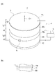
図1(a)は、実施形態に係るセンサ1の構成を示す斜視図である。(Overall configuration of sensor)
FIG. 1A is a perspective view illustrating a configuration of a
センサ1は、例えば、圧力(別の観点では力)を電気信号(別の観点では電荷または電圧)に変換するセンサ素子3と、センサ素子3に電気的に接続された配線部4と、配線部4を介してセンサ素子3に電気的に接続され、センサ素子3からの信号に対して所定の処理を施す処理部5とを有している。なお、センサ素子3がセンサ(狭義)と捉えられてもよいし、センサ素子3と配線部4との組み合わせがセンサと捉えられてもよい。
The
(センサ素子の全体構成)
センサ素子3は、例えば、概略円柱状に構成されており、その円柱の軸方向D1(便宜的に軸D1ということもある。)において受けた圧力に応じた電気信号を出力する。円柱の直径および高さは適宜に設定されてよい。例えば、直径は、高さよりも大きくてもよいし、同等でもよいし、小さくてもよい。寸法の一例を示すと、直径は、3mm以上10mm以下であり、高さは、1mm以上4mm以下である。また、例えば、直径は、高さの2倍以上5倍以下である。(Overall configuration of sensor element)
The
なお、センサ素子3は、いずれの方向が上方または下方とされてもよいものであるが、以下の説明では、便宜上、図示の軸方向D1の矢印が指す方向(紙面上方)を上方として、上面または下面等の語を用いることがある。
The
センサ素子3は、例えば、軸方向D1において積層された複数の層状部材から構成されている。複数の層状部材は、例えば、上方から順に、第1電極7A、第1圧電体9A、第2電極7B、第2圧電体9Bおよび第3電極7Cである。これらの層状部材のうち、互いに重なるもの同士(7Aと9A、9Aと7B、7Bと9B、および9Bと7C)は、その対向面において接着されている。
The
なお、以下では、第1電極7A〜第3電極7Cを区別せずに、単に「電極7」ということがある。また、第1圧電体9Aおよび第2圧電体9Bを区別せずに、単に「圧電体9」ということがある。
Hereinafter, the first electrode 7A to the
センサ素子3に軸方向D1における圧力が加えられ、ひいては、各圧電体9に軸方向D1における圧力が加えられると、各圧電体9においては圧力値に応じた強度(例えば電圧値または電荷量)の電気信号が生じる。この信号は、各圧電体9の両側に重なる1対の電極7によって取り出される。
When the pressure in the axial direction D1 is applied to the
なお、センサ素子3は、他の適宜な部材と組み合わされてよい。例えば、センサ素子3は、その下面の概ね全体に当接する部材によって支持され、上面に加えられる圧力を検出するように構成されてよい。ただし、センサ素子3は、例えば、上面の全体において支持されたり、上面、下面および/または側面の一部において支持されたり、軸方向D1の圧力によって撓み変形可能に支持されたりしてもよい。
Note that the
また、例えば、センサ素子3は、気体または液体の圧力を検出することに利用されてもよいし、力(荷重)を検出することに利用されてもよい。センサ素子3を含むセンサは、用途に応じて適宜な構造とされてよい。例えば、センサ素子3は、上面および/または下面を外部(気体中または液体中)に露出させてもよいし、2つの剛体部材に軸方向D1において挟まれてもよいし、上面および/または下面が適宜な厚さの絶縁膜に覆われてもよい。前記の剛体部材は、上面および/または下面に対してその全体に当接してもよいし、一部に当接してもよい。
Further, for example, the
(層状部材の形状および寸法)
3つの電極7および2つの圧電体9それぞれは、例えば、一様な厚さの層状である。3つの電極7および2つの圧電体9の平面形状は、例えば、互いに同一であり、本実施形態では円形である。(Shape and dimensions of layered member)
Each of the three
3つの電極7の厚さは、互いに異なっている。具体的には、第1電極7Aの厚さをt1、第2電極7Bの厚さをt2、第3電極7Cの厚さをt3とすると、t1〜t3は、下記の(1)式を満たす。
t2>t3>t1 (1)The thicknesses of the three
t2>t3> t1 (1)
2つの圧電体9の厚さtp1およびtp2(以下、両者を区別せずに「厚さtp」ということがある。)は、例えば、互いに同一である。ただし、これらの厚さtpは互いに異なっていてもよい。また、各圧電体9の厚さtpは、例えば、3つの電極7のいずれの厚さよりも厚い。換言すれば、tp>t2である。ただし、圧電体9の厚さは、3つの電極7のうち最も厚い第2電極7Bの厚さt2よりも薄くてもよい。
The thicknesses tp1 and tp2 of the two piezoelectric bodies 9 (hereinafter, sometimes referred to as “thickness tp” without distinguishing them) are the same, for example. However, these thicknesses tp may be different from each other. Further, the thickness tp of each
厚さt1〜t3およびtpの具体的な寸法は適宜に設定されてよい。一例を示すと、以下のとおりである。
t1≦10μm
50μm≦t2≦800μm
20μm≦t3≦40μm
400μm≦tp≦1600μmSpecific dimensions of the thicknesses t1 to t3 and tp may be appropriately set. An example is as follows.
t1 ≦ 10 μm
50 μm ≦ t2 ≦ 800 μm
20 μm ≦ t3 ≦ 40 μm
400 μm ≦ tp ≦ 1600 μm
また、別の観点で、寸法の一例を示すと、以下のとおりである。
t1≦0.2×t2
0.025×t2≦t3≦0.8×t2
t2≦tp≦16×t2
なお、上記の絶対値(μm)で示された範囲と、他の厚さとの大小関係で示された範囲とは適宜に組み合わされてよい。Another example of the dimensions from another viewpoint is as follows.
t1 ≦ 0.2 × t2
0.025 × t2 ≦ t3 ≦ 0.8 × t2
t2 ≦ tp ≦ 16 × t2
The range indicated by the absolute value (μm) and the range indicated by the magnitude relationship with other thicknesses may be appropriately combined.
(層状部材の材料(線膨張係数))
各電極7は、導電体からなり、例えば、金属によって構成されている。各電極7を構成する金属は、線膨張係数(熱膨張係数)およびヤング率等の力学的な性質に関して概ね等方性を有している。第1電極7Aを構成する材料は、適宜に設定されてよく、第2電極7Bまたは第3電極7Cを構成する材料と同一であってもよいし、異なっていてもよい。第2電極7Bまたは第3電極7Cを構成する材料は互いに異なっており、ひいては、その線膨張係数は互いに異なっている。(Material of layered member (linear expansion coefficient))
Each
各圧電体9は、例えば、圧電性を有する単結晶からなる。圧電体9を構成する単結晶は、線膨張係数およびヤング率等の力学的な性質に関して異方性を有している。具体的には、例えば、圧電体9は、軸方向D1に直交する面に平行な方向における線膨張係数に関して異方性を有している。2つの圧電体9は、例えば、互いに同一の材料の単結晶からなり、かつ軸方向D1と結晶軸とが成す角度が互いに同一である。
Each
圧電体9を構成する単結晶は、例えば、水晶(SiO2)である。その他、圧電体9を構成する単結晶の材料は、ニオブ酸リチウム(LiNbO3)、タンタル酸リチウム(LiTaO3)、四ほう酸リチウム(Li2B4O7)、ニオブ酸カリウム(KNbO3)またはランガサイト系化合物であってもよい。ただし、以下では、圧電体9が水晶からなることを前提として説明を行うことがある。The single crystal constituting the
第2電極7B、第3電極7Cおよび圧電体9の材料は、これらの線膨張係数が、下記の(2)式を満たす限り、適宜に選択されてよい。
α2>αmax>α3>αmin (2)
ただし、α2は第2電極7Bの線膨張係数であり、α3は第3電極7Cの線膨張係数である。また、αmaxは、圧電体9の軸方向D1に直交する面内における最も大きい線膨張係数であり、αminは、圧電体9の軸方向D1に直交する面内における最も小さい線膨張係数である。The material of the
α2> αmax >α3> αmin (2)
Here, α2 is the linear expansion coefficient of the
既述の(1)を満たすように層状部材(7および9)の厚さを設定し、かつ上記の(2)式を満たすように層状部材(7および9)の材料を選択することによって、例えば、後に詳述するように、熱応力に起因する圧電体9の破損のおそれを低減できる。
By setting the thickness of the layered members (7 and 9) so as to satisfy the above-mentioned (1) and selecting the material of the layered members (7 and 9) so as to satisfy the above expression (2), For example, as will be described in detail later, the possibility of breakage of the
上記の(2)式に代えて、以下の(2)′式が満たされるように材料の選択がなされてもよい。
α2>αmax>α3>α90 (2)′
ただし、α90は、軸方向D1に直交する面内の、αmaxとなる方向に直交する方向における圧電体9の線膨張係数である。なお、αminの定義に照らしてαmin≦α90が当然に成り立つから、(2)′式は(2)式の下位概念である。Instead of the above equation (2), the material may be selected so as to satisfy the following equation (2) ′.
α2> α max>α3> α 90 (2) '
However, alpha 90 is in a plane perpendicular to the axial direction D1, a linear expansion coefficient of the
具体的な材料を例示すると、以下のとおりである。 Specific materials are as follows.
例えば、圧電体9が水晶からなり、X軸(電気軸)、Y軸(機械軸)およびZ軸(光軸、c軸)のうち、X軸が軸方向D1に平行であるものとする。ここで、X軸方向における線膨張係数とY軸方向における線膨張係数とは同等であり、Z軸方向の線膨張係数は、X軸方向における線膨張係数およびY軸方向における線膨張係数よりも大きい。従って、圧電体9は、軸方向D1に直交する面内において、線膨張係数に関して異方性を有している。
For example, it is assumed that the
X軸方向に直交する種々の方向における線膨張係数は十分に公開されていないが、実務上、Z軸方向における線膨張係数を最小値とし、Z軸に直交する方向(X軸またはY軸)における線膨張係数を最大値として扱うことが行われている。これに倣い、Z軸方向における線膨張係数をαzとし、Z軸に直交する方向(X軸またはY軸)における線膨張係数をαxyとしたときに、αmax=αxy、αmin=αzとしてよい。The coefficients of linear expansion in various directions orthogonal to the X-axis direction are not sufficiently disclosed, but in practice, the coefficients of linear expansion in the Z-axis direction are minimized, and the directions orthogonal to the Z-axis (X-axis or Y-axis) Is treated as the maximum value. Following this, when the linear expansion coefficient in the Z-axis direction is αz, and the linear expansion coefficient in the direction (X-axis or Y-axis) perpendicular to the Z-axis is αxy, α max = αxy and α min = αz may be set. .
換言すれば、(2)式または(2)′に代えて、以下の(2)″式が満たされるように材料の選択がなされてもよい。
α2>αxy>α3>αz (2)″
なお、αmaxおよびαminの定義に照らしてαmax≧αxyおよびαmin≦αzが当然に成り立つから、(2)″式は(2)式の下位概念である。In other words, instead of the expression (2) or (2) ′, the material may be selected so that the following expression (2) ″ is satisfied.
α2>αxy>α3> αz (2) ″
It should be noted that, in view of the definitions of α max and α min , α max ≧ αxy and α min ≦ αz naturally hold, so that the expression (2) ″ is a subordinate concept of the expression (2).
αzは、約7.97ppm/℃である。αxyは、約13.4ppm/℃である。なお、水晶のヤング率は、方向等によるが、概ね、80GPa以上100GPa以下である。 αz is about 7.97 ppm / ° C. αxy is about 13.4 ppm / ° C. Note that the Young's modulus of the quartz crystal is generally from 80 GPa to 100 GPa, depending on the direction and the like.
従って、α2>αxyを満たす第2電極7Bの材料としては、例えば、以下のものを挙げることができる。なお、以下の括弧内において、αは線膨張係数を示し、Eはヤング率を示す(以下、同様。)。JISのC5210(りん青銅、α=約18ppm、E=約110GPa)、銅(α=約16.5ppm、E=約120GPa)、アルミニウム(α=約23ppm、E=約70GPa)、銀(α=約19ppm、E=約80GPa)、金(α=約14ppm、E=約80GPa)、およびJISのSUS304(ステンレス鋼、α=約18ppm、E=約200GPa)。
Therefore, as the material of the
また、αxy>α3>αzを満たす第3電極7Cの材料としては、例えば、以下のものを挙げることができる。JISのSUS430(ステンレス鋼、α=約12ppm、E=約200GPa)、鉄(α=約12ppm、E=約210GPa)、チタン(α=約8.5ppm、E=約110GPa)、白金(α=約9ppm、E=約160GPa)、パラジウム(α=約11ppm、E=約110GPa)、およびコバルト(α=約13ppm、E=約210GPa)。
Further, examples of the material of the
なお、線膨張係数等の物性値は、不純物の混入量および結晶の均一性(不均一性)等によってばらつく。従って、(2)式(または(2)′式もしくは(2)″式)が満たされるか否かは、あくまで線膨張係数の値によって決定されるのであり、例えば、上記で例示した材料であるか否かによって決定されるのではない。ただし、上記のような材料であれば、(2)式等が満たされ易い。また、上記のような材料であるか否かに基づいて、(2)式等が満たされるか否か推定されても構わない。 The physical properties such as the coefficient of linear expansion vary depending on the amount of impurities mixed and the uniformity (non-uniformity) of the crystal. Therefore, whether or not the expression (2) (or the expression (2) ′ or the expression (2) ″) is satisfied is determined only by the value of the linear expansion coefficient, and is, for example, the material exemplified above. However, if the material is as described above, it is easy to satisfy Expression (2), etc. Further, based on whether or not the material is as described above, (2) ) It may be estimated whether the equation or the like is satisfied.
寸法または線膨張係数の測定方法は、従来から種々のものが提案されており、そのいずれが用いられてもよい。例えば、その測定精度として、0.1ppm/℃が保証されている(0.01ppm/℃以下の誤差は存在し得る)測定方法および機器が使用されてよい。各層状部材の厚さ(t1〜t3等)は、完成後のセンサ素子3において測定されてもよいし、接着される前の状態で測定されてもよい。同様に、各層状部材の線膨張係数は、完成後のセンサ素子3を分解して測定されてもよいし、接着される前の状態で測定されてもよい。
Various methods have been proposed for measuring the dimension or the coefficient of linear expansion, and any of them may be used. For example, a measurement method and an instrument whose guaranteed accuracy is 0.1 ppm / ° C. (an error of 0.01 ppm / ° C. or less may exist) may be used. The thickness (t1 to t3, etc.) of each layered member may be measured in the
既に言及したように、第1電極7Aの材料は、適宜に設定されてよい。すなわち、第1電極7Aの線膨張係数α1は適宜に設定されてよい。例えば、α1<αminであってもよいし、α1>α2であってもよいし、α2≧α1≧αminであってもよい。As already mentioned, the material of the first electrode 7A may be appropriately set. That is, the linear expansion coefficient α1 of the first electrode 7A may be appropriately set. For example, <it may be a α min, α1> α1 may be a [alpha] 2, may be α2 ≧ α1 ≧ α min.
(層状部材同士の接着)
図1(b)は、図1(a)の領域Ibの拡大図である。なお、図1(b)は、第2電極7Bと第2圧電体9Bとの間の構成を示しているが、他の互いに重なる電極7と圧電体9との間の構成も同様である。(Adhesion between layered members)
FIG. 1B is an enlarged view of a region Ib in FIG. Although FIG. 1B shows the configuration between the
互いに重なる電極7と圧電体9とは、例えば、その間に介在する導電性の接合材11によって接着されている。接合材11の材料は、例えば、狭義のはんだ(Sn−Pb系)または鉛フリーはんだである。鉛フリーはんだとしては、例えば、Au−Sn系、Au−Si系、Au−Ge系、Sn−Cu系、Sn−Ag系、およびSn−Ag−Cu系を挙げることができる。
The
接合材11の厚さtjは、電極7の厚さおよび圧電体9の厚さに比較して薄くされている。例えば、第2電極7Bの厚さt2が50μm以上、かつ第3電極7Cの厚さt3が20μm以上であるのに対して、接合材11の厚さtjは10μm未満である。別の観点では、例えば、接合材11の厚さtjは、0.2×t2未満および/または0.5×t3未満である。従って、軸方向D1に直交する方向の熱応力に関して接合材11の影響は小さい。
The thickness tj of the bonding material 11 is smaller than the thickness of the
(配線部4および処理部5)
配線部4は、例えば、第1電極7Aと第3電極7Cとを接続している。そして、第1電極7Aおよび第3電極7Cとの組み合わせと、第2電極7Bとを処理部5の不図示の互いに異なる端子に接続している。すなわち、第1圧電体9Aおよびその両側の電極7(7Aおよび7B)からなるセンサ素子(符号省略)と、第2圧電体9Bおよびその両側の電極7(7Bおよび7C)からなるセンサ素子(符号省略)とは、処理部5に対して並列接続されている。(
The
配線部4は、各電極7の適宜な位置に対して接続されてよい。例えば、配線部4は、第1電極7Aに対しては、その上面に接続されており、第2電極7Bおよび第3電極7Cに対しては、その側面に接続されている。ただし、例えば、配線部4は、第1電極7Aの側面に接続されたり、第3電極7Cの下面に接続されたりしてもよい。
The
配線部4の構造は、適宜なものとされてよい。例えば、配線部4は、ケーブル、ボンディングワイヤーおよび/または回路基板に形成された導体パターンによって構成されてよい。その材料も適宜であるし、電極7または処理部5の端子との接続方法も適宜である。
The structure of the
処理部5は、例えば、IC(Integrated Circuit)によって構成されている。特に図示しないが、例えば、処理部5は、センサ素子3からの信号を増幅する増幅器、センサ素子3からの信号をフィルタリングするフィルタ、センサ素子3からの信号を他の形式の信号に変換する変換部(例えばAD変換器および/または変調器)、および/またはセンサ素子3からの信号に含まれる情報に対して所定の演算を施す演算部を有している。また、処理部5は、例えば、前記のような処理(増幅、フィルタリング、形式変換および/または演算)が施された信号を他の機器へ出力する出力部を有している。
The
(センサ素子の製造方法)
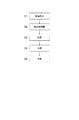
図2は、センサ素子3の製造方法の手順の一例を示すフローチャートである。(Sensor element manufacturing method)
FIG. 2 is a flowchart illustrating an example of a procedure of a method for manufacturing the
まず、ステップS1では、センサ素子3を構成する複数の層状部材(7A〜7C、9Aおよび9B)それぞれを形成する。例えば、各電極7は、圧延加工された金属板に対して打ち抜きまたはエッチングを行うことによって作製される。また、例えば、圧電体9は、人工水晶を所定のカット角でスライスして得られたウェハに対してエッチングを行うことによって作製される。
First, in step S1, a plurality of layered members (7A to 7C, 9A and 9B) constituting the
ステップS2では、圧電体9および/または電極7に接合材11を配置する。例えば、接合材11となる金属ペーストをスクリーン印刷によって圧電体9の上下面に印刷する。
In step S2, the bonding material 11 is disposed on the
ステップS3では、センサ素子3を構成する全ての圧電体9および電極7を積層する。このときの圧電体9および電極7の軸方向D1に直交する方向の位置決めは、例えば、従来公知の積層機によって、圧電体9および電極7の側面(外縁)に位置決め部材を当接させることなどにより行われる。なお、軸D1回りの位置合わせは、例えば、行われない。
In step S3, all the
ステップS4では、圧電体9および電極7からなる積層体を加熱する。これにより、接合材11が溶融される。積層体の加熱は、例えば、リフロー炉によってなされてよい。
In step S4, the laminated body including the
ステップS5では、圧電体9および電極7からなる積層体を冷却する。これにより、溶融していた接合材11が固化し、互いに重なっている圧電体9と電極7とが接着される。なお、冷却は、例えば、常温においてなされてよく、特別な装置は必ずしも必要ではない。
In step S5, the laminated body including the
上記のステップS5において、接合材11は、その温度が凝固点に到達すると固化する。通常、接合材11の凝固点は常温よりも高いから、比較的高い温度で圧電体9と電極7とは接着されることになる。例えば、Au−Sn(20wt%Sn)の場合、凝固点は約280℃である。そして、センサ素子3は、ステップS5において、またはその後において、常温に晒されるから、センサ素子3においては、凝固点から常温になるまでの温度変化によって熱応力が生じることになる。
In the above step S5, the bonding material 11 solidifies when its temperature reaches the solidification point. Normally, since the solidification point of the bonding material 11 is higher than room temperature, the
(圧電体に生じる熱応力)
(1)式を満たすように層状部材(7および9)の厚さを設定し、かつ上記の(2)式、(2)′式または(2)″式を満たすように層状部材(7および9)の材料を選択することによって、例えば、熱応力に起因する圧電体9の破損のおそれを低減できる。この作用について以下に説明する。(Thermal stress generated in the piezoelectric body)
The thickness of the layered members (7 and 9) is set so as to satisfy the expression (1), and the layered members (7 and 9) are set so as to satisfy the above expression (2), (2) ′ or (2) ″. By selecting the material of 9), for example, the risk of breakage of the
ここでは、図2を参照して説明したように、比較的高い温度(例えば常温よりも高い温度)で圧電体9と電極7とが接着され、その後、これらの部材が相対的に低い温度(例えば常温)とされた場合を想定する。
Here, as described with reference to FIG. 2, the
(電極と圧電体との間の熱応力)
図3(a)〜図3(f)は、電極7の厚さおよび線膨張係数が電極7と圧電体9との間に生じる熱応力に及ぼす影響を説明するための模式図である。ここでは、1つの圧電体9と、その両側に位置する2つの電極7とからなる構成を想定する。従って、例えば、2つの圧電体9間の力学的な相互影響は考慮しない。(Thermal stress between electrode and piezoelectric body)
FIGS. 3A to 3F are schematic diagrams for explaining the effect of the thickness and the coefficient of linear expansion of the
図3(a)、図3(c)および図3(e)は、圧電体9およびその両側の電極7を示す斜視図である。これらの図は、電極7の厚さおよび線膨張係数が互いに異なる態様を示している。具体的には、図3(a)では電極7が比較的薄くされているのに対して、図3(c)および図3(e)では電極7が比較的厚くされている。また、図3(c)では、電極7の線膨張係数(αe)が比較的大きくされている(例えばαe>αmax)のに対して、図3(e)では、電極7の線膨張係数(αe)が比較的小さくされている(例えばαe<αmin(α90))。3 (a), 3 (c) and 3 (e) are perspective views showing the
図3(b)、図3(d)および図3(f)は、圧電体9と電極7との線膨張係数の相違に起因して圧電体9に生じる熱応力を説明するための模式図であり、それぞれ、図3(a)、図3(c)および図3(e)の態様に対応している。これらの図においては、圧電体9が示されているとともに、熱応力のうち引張応力が大きい領域にハッチングが付されている。なお、図3(b)、図3(d)および図3(f)は、シミュレーション計算結果に基づいている。
FIGS. 3B, 3D, and 3F are schematic diagrams for explaining thermal stress generated in the
図3(a)および図3(b)に示すように、電極7の厚さが比較的薄い場合においては、圧電体9に生じる熱応力は小さい。このことは、電極7の線膨張係数が圧電体9の線膨張係数に対して大きくても、小さくても同様である。
As shown in FIGS. 3A and 3B, when the thickness of the
図3(c)および図3(d)に示すように、電極7の厚さが比較的厚く、かつ電極7の線膨張係数αeが圧電体9の線膨張係数(例えばαmax)よりも大きい場合においては、温度が低下するときの収縮量は、圧電体9よりも電極7の方が大きい。従って、基本的には、圧電体9は、電極7から圧縮力を受けることになる。すなわち、基本的には、圧電体9において引張応力は小さい。As shown in FIGS. 3C and 3D, the thickness of the
ただし、圧電体9は、その上下面が当該上下面に沿う方向の圧縮力を電極7から受けることから、その側面に引張応力が生じる。別の観点では、ポアソン効果が生じる。より具体的には、圧電体9は、軸方向D1に直交する方向における線膨張係数に関して異方性を有していることから、その側面のうち、線膨張係数が相対的に小さい方向の両側となる領域R1においては、他の領域R2に比較して相対的に引張応力が大きくなる。
However, since the upper and lower surfaces of the
図3(e)および図3(f)に示すように、電極7の厚さが比較的厚く、かつ電極7の線膨張係数αeが圧電体9の線膨張係数(例えばαmin(α90))よりも小さい場合においては、温度が低下するときの収縮量は、電極7よりも圧電体9の方が大きい。従って、基本的に、圧電体9は、電極7から引張力を受けることになる。より具体的には、圧電体9の上下面に相対的に高い引張応力が生じる。なお、図3(f)におけるハッチングと応力の大きさとの相対関係では、図に現れていないが、より具体的には、圧電体9の線膨張係数に関する異方性に起因して、引張応力は、線膨張係数が相対的に大きい方向の両側において相対的に高くなる。As shown in FIGS. 3E and 3F, the thickness of the
(圧電体間の熱応力)
図4(a)は、2つの圧電体9間において熱応力が生じる理由を説明するための模式図である。(Thermal stress between piezoelectric bodies)
FIG. 4A is a schematic diagram for explaining the reason why thermal stress occurs between two
この図において、各圧電体9に付されたX軸、Y軸およびZ軸は、水晶のX軸(電気軸)、Y軸(機械軸)およびZ軸(光軸、c軸)を示している。2つの圧電体9は、いずれも水晶から構成されており、互いに同一のカット角で(ここではX軸に直交する角度で)切り出されている。
In this figure, an X axis, a Y axis and a Z axis attached to each
ここで、既に述べたように、水晶は、YZ平面において、線膨張係数に関して異方性を有している。従って、2つの圧電体9を互いに貼り合わせるときに、図示の例のようにX軸回りの位置が互いにずれると、XZ平面内の任意の方向における温度低下に対する縮小量が互いに異なることになる。その結果、2つの圧電体9が互いに同一のカット角の水晶から構成されていても(軸D1と結晶軸との成す角度が2つの圧電体9間で同一であっても)、2つの圧電体9間において熱応力が生じる。
Here, as described above, quartz has anisotropy in linear expansion coefficient in the YZ plane. Therefore, when the two
図4(b)〜図4(e)は、電極7の厚さが2つの圧電体9間に生じる熱応力に及ぼす影響を説明するための模式図である。ここでは、図4(a)に示されているように、2つの圧電体9間において、X軸回りの回転位置が互いに90°ずれている場合を想定する。また、ここでは、2つの圧電体9と、その間の第2電極7Bとからなる構成を想定する。従って、第1電極7Aおよび第3電極7Cが熱応力に及ぼす影響は考慮しない。
FIGS. 4B to 4E are schematic diagrams for explaining the effect of the thickness of the
図4(b)および図4(d)は、2つの圧電体9およびその間の第2電極7Bを示す斜視図である。これらの図は、第2電極7Bの厚さが互いに異なる態様を示している。具体的には、図4(b)では第2電極7Bが比較的薄くされているのに対して、図4(d)では第2電極7Bが比較的厚くされている。なお、これらの図において、第2電極7Bの線膨張係数は、αminよりも大きく、αmaxよりも小さい。FIGS. 4B and 4D are perspective views showing two
図4(c)および図4(e)は、圧電体9(ここでは第2圧電体9Bを図示)に生じる熱応力を説明するための模式図であり、それぞれ、図4(b)および図4(d)の態様に対応している。これらの図においては、圧電体9が示されているとともに、熱応力のうち引張応力が大きい領域にハッチングが付されている。なお、図4(c)および図4(e)は、シミュレーション計算結果に基づいている。
FIGS. 4C and 4E are schematic diagrams for explaining thermal stress generated in the piezoelectric body 9 (here, the second
図4(b)および図4(c)に示すように、第2電極7Bの厚さが比較的薄い場合においては、圧電体9の他の圧電体9側の面において比較的高い引張応力が比較的広い範囲に亘って生じる。なお、図4(c)におけるハッチングと応力の大きさとの相対関係では、図に現れていないが、より具体的には、各圧電体9において、引張応力は、線膨張係数が相対的に大きい方向の両側において相対的に高くなる。また、特に図示しないが、圧縮応力は、各圧電体9の側面付近、かつ線膨張係数が相対的に小さい方向の両側において大きくなる。
As shown in FIGS. 4B and 4C, when the thickness of the
図4(d)および図4(e)に示すように、第2電極7Bの厚さが比較的厚い場合においては、圧電体9に生じる引張応力(および圧縮応力)は比較的小さい。
As shown in FIGS. 4D and 4E, when the thickness of the
上記のことから、第2電極7Bが比較的薄い場合においては、2つの圧電体9間の熱応力によって引張応力が比較的大きくなり、第2電極7Bが比較的厚い場合においては、2つの圧電体9間の引張応力が緩和されることがわかる。
From the above, when the
(実施形態における熱応力)
本実施形態では、(1)式に示されているように、2つの圧電体9間に位置する第2電極7Bの厚さt2が他の電極7の厚さt1およびt3よりも厚い。従って、例えば、図4(b)〜図4(d)を参照して説明したように、圧電体9の軸方向D1に直交する面内における線膨張係数に関する異方性および2つの圧電体9間の軸D1回りの位置ずれに起因して圧電体9に生じる引張応力を緩和することができる。(Thermal stress in the embodiment)
In the present embodiment, as shown in the expression (1), the thickness t2 of the
この厚くされた第2電極7Bの線膨張係数α2は、(2)式(または(2)′もしくは(2)″式)に示されているように、圧電体9の軸方向D1に直交する面内における最大の線膨張係数αmaxよりも大きい。従って、例えば、図3(c)および図3(d)の説明からも理解されるように、圧電体9が第2電極7Bから受ける力は、基本的には圧縮力となる。その結果、例えば、第2電極7Bが厚くされることに起因して圧電体9に生じる引張応力が大きくなるおそれは低減される。The linear expansion coefficient α2 of the thickened
また、図3(a)〜図3(f)を参照して説明したように、圧電体9の両側の電極7が厚くなると、電極7の線膨張係数αeが圧電体9の線膨張係数に比較して大きくても、小さくても、引張応力が大きくなる。一方、本実施形態では、(1)式に示されているように、第1電極7Aの厚さt1および第3電極7Cの厚さt3を第2電極7Bの厚さt2よりも薄くして、圧電体9の両側の電極7の双方が厚くされないようにしている。さらに、(2)(または(2)′もしくは(2)″式)に示されているように、3つの電極7のうち2番目の厚さの第2電極7Bの線膨張係数α2を圧電体9の線膨張係数の最大値と最小値との間の値となるようにしている。従って、圧電体9に生じる引張応力を更に低減することができる。
Further, as described with reference to FIGS. 3A to 3F, when the
ここで、圧電体9は、一般に、圧縮力による破損よりも引張力による破損が生じやすい。従って、上記のように圧電体9に生じる引張応力を低減することによって、圧電体9の破損のおそれを低減することができる。
Here, the
なお、第1電極7Aの厚さt1は、3つの電極7のうち最も薄いことから((1)式)、圧電体9との間で生じる熱応力が最も小さい。従って、第2電極7Bおよび第3電極7Cの線膨張係数α2およびα3に比較して、第1電極7Aの線膨張係数α1の設計の自由度は高く、適宜に設定されてよい。
Since the thickness t1 of the first electrode 7A is the thinnest among the three electrodes 7 (formula (1)), the thermal stress generated between the first electrode 7A and the
また、第3電極7Cが第1電極7Aよりも厚いことによって((1)式)、例えば、配線部4を第1電極7Aの上面に接続する一方で、配線部4を第3電極7Cの側面に接続することができる。従って、例えば、センサ素子3の下面を支持するようにセンサ素子3を配置することが容易化される。
Further, since the
(実施例)
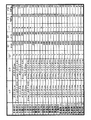
図5は、比較例および実施例に係るセンサ素子の構成および熱応力を示す図表である。(Example)
FIG. 5 is a chart showing the configurations and thermal stresses of the sensor elements according to the comparative example and the example.
比較例1〜8および実施例1〜18は、センサ素子3について、具体的な材料および寸法が設定されたものである。そして、その材料および寸法に基づいて、シミュレーション計算によって、圧電体9等に生じる熱応力を求めた。
In Comparative Examples 1 to 8 and Examples 1 to 18, specific materials and dimensions of the
(比較例および実施例に共通の条件)
全ての比較例および実施例に共通する条件は、以下のとおりである。
センサ素子3の直径:4mm
第1電極7A:
材料:Au
厚さt1:5μm
圧電体9:
材料:水晶(X軸と軸方向D1とが平行)
厚さtp:700μm
2つの圧電体間におけるX軸回りのずれ量:90°
接合材11:
材料:AuSn
厚さ:5μm(Common conditions for Comparative Examples and Examples)
Conditions common to all the comparative examples and examples are as follows.
Diameter of sensor element 3: 4 mm
First electrode 7A:
Material: Au
Thickness t1: 5 μm
Piezoelectric body 9:
Material: Quartz (X axis and axial direction D1 are parallel)
Thickness tp: 700 μm
Displacement around the X axis between two piezoelectric bodies: 90 °
Bonding material 11:
Material: AuSn
Thickness: 5 μm
水晶の弾性定数はテンソル量で考慮し、以下のように設定した。なお、以下において単位はGPaである。c11=86.72、c12=6.89、c13=11.88、c14=−17.92、c15=0、c16=0、c22=86.72、c23=11.88、c24=17.92、c25=0、c26=0、c33=107.12、c34=0、c35=0、c36=0、c44=57.89、c45=0、c46=0、c55=57.89、c56=−17.92、c66=39.92。 The elastic constant of quartz was set as follows, taking into account the amount of tensor. In the following, the unit is GPa. c11 = 86.72, c12 = 6.89, c13 = 11.88, c14 = -17.92, c15 = 0, c16 = 0, c22 = 86.72, c23 = 11.88, c24 = 17.92 , C25 = 0, c26 = 0, c33 = 107.12, c34 = 0, c35 = 0, c36 = 0, c44 = 57.89, c45 = 0, c46 = 0, c55 = 57.89, c56 = − 17.92, c66 = 39.92.
水晶の線膨張係数は、Z軸方向を7.97ppm/℃とし、Z軸に直交する方向を13.4ppm/℃とした。また、その他の方向における線膨張係数については、上記のZ軸方向およびこれに直交する方向の線膨張係数に基づく補間によって算出した。 The linear expansion coefficient of the crystal was 7.97 ppm / ° C. in the Z-axis direction and 13.4 ppm / ° C. in the direction perpendicular to the Z-axis. Further, the linear expansion coefficients in other directions were calculated by interpolation based on the linear expansion coefficients in the Z-axis direction and the direction orthogonal thereto.
接合材11は、280℃で固化するものとした。すなわち、280℃から常温(20℃)まで温度が低下することを想定して、熱応力を算出した。 The bonding material 11 solidified at 280 ° C. That is, the thermal stress was calculated on the assumption that the temperature would decrease from 280 ° C. to room temperature (20 ° C.).
なお、第1電極7Aの厚さt1および接合材11の厚さは、圧電体9の厚さtpに比較して十分に薄く、第1電極7Aおよび接合材11が熱応力に及ぼす影響は十分に小さい。また、センサ素子3の直径は、センサ素子3内の各層の厚さおよび線膨張係数が軸方向D1に直交する方向における熱応力に及ぼす定性的な影響とは基本的に独立している。
The thickness t1 of the first electrode 7A and the thickness of the bonding material 11 are sufficiently smaller than the thickness tp of the
(比較例および実施例毎の条件)
比較例および実施例間では、第2電極7Bの材料(線膨張係数α2)および厚さt2、ならびに第3電極7Cの材料(線膨張係数α3)および厚さt3に係る条件を互いに異ならせた。(Conditions for Comparative Examples and Examples)
The conditions relating to the material (linear expansion coefficient α2) and thickness t2 of the
具体的には、大きな分類として、(1)式が満たされている条件と満たされていない条件との2種と、(2)′式が満たされている条件と満たされていない条件との2種との組み合わせの合計4種(2種×2種)を設定した。 Specifically, there are two major classifications: a condition that satisfies Expression (1) and a condition that is not satisfied, and a condition that satisfies Expression (2) ′ and a condition that Expression (2) ′ is not satisfied. A total of 4 types (2 types × 2 types) in combination with 2 types were set.
図5の「(2)′」の欄において、「Y」は(2)′式が満たされていることを示し、「N」は(2)′式が満たされていないことを示している。同様に、図5の「(1)」の欄において、「Y」は(1)式が満たされていることを示し、「N」は(1)式が満たされていないことを示している。従って、実施例においては、「(2)′」および「(1)」の双方が「Y」であり、比較例においては、「(2)′」および「(1)」の少なくとも一方が「N」である。 In the column of "(2) '" in FIG. 5, "Y" indicates that the expression (2)' is satisfied, and "N" indicates that the expression (2) 'is not satisfied. . Similarly, in the column of “(1)” in FIG. 5, “Y” indicates that Expression (1) is satisfied, and “N” indicates that Expression (1) is not satisfied. . Therefore, in the example, both “(2) ′” and “(1)” are “Y”, and in the comparative example, at least one of “(2) ′” and “(1)” is “Y”. N ".
図5の「α2」は、第2電極7Bの線膨張係数α2と、圧電体9の線膨張係数αmaxおよびα90との大小関係を示している。同様に、図5の「α3」は、第3電極7Cの線膨張係数α3と、圧電体9の線膨張係数αmaxおよびα90との大小関係を示している。“Α2” in FIG. 5 indicates a magnitude relationship between the linear expansion coefficient α2 of the
これらの欄から理解されるように、(2)′式が満たされない条件としては、より具体的には、α2およびα3の双方がαmaxよりも大きくなるもの(比較例1および5)、α2およびα3の双方がα90よりも小さくなるもの(比較例3)、α2およびα3の双方がαmaxとα90との間の大きさとなるもの(比較例2および6)を設定した。As can be understood from these columns, as the condition (2) 'equation is not satisfied, more specifically, those both [alpha] 2 and α3 is greater than the alpha max (Comparative Examples 1 and 5), [alpha] 2 and that both α3 is smaller than the alpha 90 (Comparative example 3), both the α2 and α3 is set what the size (Comparative examples 2 and 6) between the alpha max and alpha 90.
比較例および実施例において、α(α2またはα3)がαmaxよりも大きくなる電極7(7Bまたは7C)の材料としては、C5210(α=18.2、E=110GPa、ν=0.33)を想定した。なお、νはポアソン比である(以下、同様。)。αがαminよりも小さくなる電極7の材料としては、JISの42alloy(42wt%NiのNiFe合金、α=5.5、E=144GPa、ν=0.25)を想定した。αがαmaxとα90との間の大きさとなる電極7の材料としては、SUS430(α=11.9、E=200GPa、ν=0.3)を想定した。In Comparative Examples and Examples, alpha ([alpha] 2 or .alpha.3) is greater than the alpha max electrode 7 as a material for the (7B or 7C), C5210 (α = 18.2 , E = 110GPa, ν = 0.33) Was assumed. Here, ν is a Poisson's ratio (the same applies hereinafter). As a material of the
図5の「t2」および「t3」の欄は、厚さt2およびt3の値を示している。(1)式が満たされない条件としては、より具体的には、t2=t3を設定した。比較例および実施例において、t2は30μm以上800μm以下の範囲で設定した。t3は30μm以上200μm以下の範囲で設定した。なお、t2/t3は、1以上26.7未満となっている。 The columns “t2” and “t3” in FIG. 5 show values of the thicknesses t2 and t3. More specifically, the condition that the expression (1) is not satisfied is set to t2 = t3. In Comparative Examples and Examples, t2 was set in the range of 30 μm or more and 800 μm or less. t3 was set in the range of 30 μm or more and 200 μm or less. Note that t2 / t3 is 1 or more and less than 26.7.
(熱応力の計算結果)
図5の「σ1」の欄は、シミュレーション計算によって得られた、第1圧電体9Aに生じる引張応力(熱応力)の最大値を示している。同様に、図5の「σ2」の欄は、シミュレーション計算によって得られた、第2圧電体9Bに生じる引張応力(熱応力)の最大値を示している。(Calculation results of thermal stress)
The column of “σ1” in FIG. 5 shows the maximum value of the tensile stress (thermal stress) generated in the first
この欄に示されているように、全ての実施例は、σ1およびσ2の双方が48MPa以下となっている。一方、全ての比較例は、σ1およびσ2の少なくとも一方が49MPa以上となっている。この結果から、(1)式および(2)′式が満たされることによって、2つの圧電体9の双方に生じる引張応力の最大値を低下させることができることが確認できる。
As shown in this column, in all the examples, both σ1 and σ2 are 48 MPa or less. On the other hand, in all the comparative examples, at least one of σ1 and σ2 is 49 MPa or more. From this result, it can be confirmed that, by satisfying the expressions (1) and (2) ′, the maximum value of the tensile stress generated in both of the two
また、例えば、比較例1〜7および実施例1の比較から、第2電極7B(厚さt2)および第3電極7C(厚さt3)の双方を厚くすると(比較例1〜4)、その間に挟まれている第2圧電体9Bの引張応力σ2が大きくなってしまうことが確認できる。また、第2電極7B(厚さt2)および第3電極7C(厚さt3)の双方を薄くすると(比較例5〜7)、2つの圧電体9間の熱応力が大きくなり、2つの圧電体9の双方の引張応力(σ1およびσ2)が大きくなってしまうことが確認できる。
Also, for example, from a comparison between Comparative Examples 1 to 7 and Example 1, when both the
なお、このシミュレーション計算では、t2<t3の場合について示されていない。ただし、この場合、t2が薄くなることによって比較例5〜7のように2つの圧電体9の双方の引張応力が大きくなり、かつt3が厚くなることによって第2圧電体9Bの引張応力が大きくなるから、実施例の方が引張応力を小さくできることは明らかである。
Note that this simulation calculation does not show the case where t2 <t3. However, in this case, the tensile stress of both
また、例えば、比較例1〜4の比較から、第2電極7Bおよび第3電極7Cの双方の線膨張係数(α2およびα3)を小さくすると(比較例3)、圧電体9の方がこれらの電極7よりも収縮量が大きいから引張応力が大きくなってしまうことが確認できる。第2電極7Bおよび第3電極7Cの双方の線膨張係数を大きくすると(比較例1)、その間に挟まれた第2圧電体9Bにおいて大きな引張応力が生じてしまうことが確認できる。
Also, for example, from the comparison of Comparative Examples 1 to 4, when the linear expansion coefficients (α2 and α3) of both the
また、例えば、第2電極7Bおよび第3電極7Cの双方が厚い場合においては(比較例1〜比較例4)、第2電極7Bおよび第3電極7Cの双方の線膨張係数(α2およびα3)をαmaxとα90との間の大きさとすると(比較例2)、(2)′式が満たされる場合(比較例4)よりも、σ1およびσ2の双方に関する最大値は小さくなる(比較例2のσ2が78MPaであるのに対して比較例4のσ4は81MPa)。このことから、(2)′式は、(1)式との組み合わせによってその作用効果が顕著になるものであることが確認できる。Further, for example, when both the
なお、第2電極7Bおよび第3電極7Cの双方が薄い場合においては(比較例5〜比較例7)、2つの圧電体9間の熱応力が大きくなるから、α2およびα3をαmaxとα90との間の大きさとしても(比較例6)、(2)′式が満たされる場合(比較例7)よりも、σ1およびσ2の双方に関する最大値は小さくなるとは限らない。When both the
以上のとおり、センサ1(センサ素子3)は、第1電極7A、第1圧電体9A、第2電極7B、第2圧電体9Bおよび第3電極7Cを、この列挙順を積層方向(軸方向D1)における順番として積層的に、かつ互いに重なるもの同士が接着された状態で有している。第1圧電体9Aおよび第2圧電体9Bは、同一の材料の単結晶からなり、かつ軸方向D1と結晶軸とが成す角度が同一である。圧電体9を構成する単結晶は、軸方向D1に直交する面内の線膨張係数に関して異方性を有している。そして、センサ1では、上述の(1)式および(2)式が満たされる。
As described above, the sensor 1 (sensor element 3) arranges the first electrode 7A, the first
従って、図3および図4を参照して説明したように、例えば、電極7と圧電体9とが比較的高温で接着されて冷却されるときに(ステップS4およびS5)、両者の線膨張係数の差に起因して圧電体9に大きな引張応力が加えられるおそれが低減される。ひいては、圧電体9が破損するおそれが低減される。また、例えば、製造後においても、センサ素子3の温度変化が繰り返されたときに圧電体9に大きな引張応力が繰り返し加えられるおそれが低減されるから、耐久性が向上する。
Therefore, as described with reference to FIGS. 3 and 4, for example, when the
なお、α2およびα3等の線膨張係数の設定は、実際には、具体的な材料の選択によって実現される。従って、例えば、α2およびα3に係る条件の相違は、第2電極7Bおよび第3電極7Cのヤング率に係る条件の相違も伴っている。一方、熱応力には、線膨張係数だけでなく、ヤング率も影響している。しかし、図3および図4を参照して説明した、電極3の線膨張係数と圧電体9の線膨張係数との大小関係と、圧電体9における応力分布との定性的な関係は、ヤング率に依存しない。従って、ヤング率を考慮しなくても、(2)式(または(2)′式もしくは(2)″式)を満たすように材料を選択することによって、圧電体9に生じる引張応力(その最大値)を低減できることに変わりはない。
The setting of the coefficient of linear expansion such as α2 and α3 is actually realized by selecting a specific material. Therefore, for example, the difference in the conditions related to α2 and α3 is accompanied by the difference in the condition related to the Young's modulus of the
また、比較例1〜4を参照して既に述べたように、電極7が比較的厚く、電極7の熱膨張係数が圧電体9に生じる熱応力に及ぼす影響が相対的に大きい場合においては、線膨張係数が水晶(圧電体9)の線膨張係数αmaxとα90との間の大きさであるときにσ1およびσ2の双方に関する最大値が小さくなった(比較例4)。ここで、比較例1〜4において、線膨張係数が水晶(圧電体9)の線膨張係数αmaxとα90との間の大きさとなる電極7の材料は、他の電極7の材料に比較して最もヤング率が大きく、ヤング率の観点からは圧電体9に及ぼす熱応力が大きくなりやすいものである。すなわち、ヤング率の観点からは圧電体9に及ぼす熱応力が最も大きくなりやすい比較例3において引張応力が小さかったことになる。従って、図5のシミュレーション結果においてヤング率の影響は小さいと考えてもよいし、あるいはヤング率を考慮しても、(1)式および(2)式(または(2)′式もしくは(2)″式)を満たすように材料を選択することによって引張応力を小さくすることがシミュレーション計算によって確認されたと考えてもよい。Further, as already described with reference to Comparative Examples 1 to 4, when the
また、本実施形態では、第1圧電体9Aおよび第2圧電体9Bは、電気軸(X軸)が積層方向(軸方向D1)に平行な水晶からなる。
In the present embodiment, the first
従って、例えば、圧電体9が水晶である場合における第2電極7Bおよび第3電極7Cの材料の例示(既述)から理解されるように、(2)式(または(2)′式もしくは(2)″式)を満たす材料として、電子部品に一般的に用いられている材料を選択しやすい。
Therefore, for example, as understood from the examples of the materials of the
また、本実施形態では、第1圧電体9Aおよび第2圧電体9Bの厚さをtp1およびtp2としたときに、
t2≦tp1≦16×t2、
t2≦tp2≦16×t2、
50μm≦t2≦800μm、かつ
20μm≦t3≦40μm、であるIn this embodiment, when the thicknesses of the first
t2 ≦ tp1 ≦ 16 × t2,
t2 ≦ tp2 ≦ 16 × t2,
50 μm ≦ t2 ≦ 800 μm and 20 μm ≦ t3 ≦ 40 μm
このような範囲であれば、実施形態の効果をより確実に奏することができる。なお、t2≦tp(tp1、tp2)≦16×t2および50μm≦t2≦800μmは、実施例1〜18におけるtpおよびt2の範囲である。t3については、実施例1〜18では、30μmまたは40μmであるが、t2とは異なり、t3が小さいほど圧電体9の引張応力が小さくなることは明らかである。ただし、t3が20μm以上であれば、例えば、取り扱いが容易である。
Within such a range, the effects of the embodiment can be achieved more reliably. Note that t2 ≦ tp (tp1, tp2) ≦ 16 × t2 and 50 μm ≦ t2 ≦ 800 μm are the ranges of tp and t2 in Examples 1 to 18. Although t3 is 30 μm or 40 μm in Examples 1 to 18, it is apparent that, unlike t2, the smaller the t3, the lower the tensile stress of the
また、本実施形態では、第1圧電体9Aおよび第2圧電体9Bは、積層方向(軸方向D1)に見て、互いに同一の形状であるとともに、nを3以上としたときにn回対称の形状(360°/nで回転させたときに自らと重なる回転対称の形状、本実施形態では円形)である。
Further, in the present embodiment, the first
すなわち、2つの圧電体9は、軸D1回りに位置ずれが生じやすい形状である。このような場合においては、2つの圧電体9間で軸D1に直交する方向において線膨張係数が互いに異なりやすい。従って、例えば、第2電極7Bを厚くすることによって2つの圧電体9間の熱応力を緩和する効果が奏され易い。なお、2つの圧電体9が回転対称の形状でなくても、例えば、製造誤差によって結晶軸の方向と形状とのずれが生じるから、本開示に係る効果は奏される。
That is, the two
本発明は、以上の実施形態に限定されず、種々の態様で実施されてよい。 The present invention is not limited to the above embodiments, and may be implemented in various modes.
センサ素子の形状は円柱状に限定されない。例えば、センサ素子の積層方向に直交する断面の形状は、回転対称の形状でなくてもよいし、2回対称の形状であってもよいし、正多角形のようにn回対称の形状(nは2以上または3以上)であってもよいし、環状であってもよい。また、センサ素子の積層方向に直交する断面の形状は、積層方向において一定でなくてもよい。 The shape of the sensor element is not limited to a column. For example, the shape of the cross section orthogonal to the stacking direction of the sensor elements may not be a rotationally symmetric shape, may be a two-fold symmetric shape, or may be an n-fold symmetric shape such as a regular polygon ( n may be 2 or more or 3 or more) or may be cyclic. Further, the shape of the cross section orthogonal to the stacking direction of the sensor elements may not be constant in the stacking direction.
圧電体の材料は、実施形態においても例示したように水晶でなくてもよい。また、カット角も適宜に設定されてよい。例えば、圧電体は、いわゆるATカットの水晶板であってもよい。 The material of the piezoelectric body does not have to be quartz as exemplified in the embodiment. Further, the cut angle may be appropriately set. For example, the piezoelectric body may be a so-called AT-cut quartz plate.
1つの電極(第1電極〜第3電極のそれぞれ)は、多層の導電層(金属層)から構成されていてもよい。また、実施形態の接合材11は、電極の一部として捉えられてもよい。このような場合、電極の線膨張係数は、電極として捉えられる層の全体としての値を用いて、本開示の要件が満たされるか否か判定すればよい。 One electrode (each of the first electrode to the third electrode) may be composed of multiple conductive layers (metal layers). Further, the bonding material 11 of the embodiment may be regarded as a part of the electrode. In such a case, the linear expansion coefficient of the electrode may be determined using the value of the entire layer regarded as the electrode as to whether or not the requirements of the present disclosure are satisfied.
接合材11は、必須の要件ではなく、例えば、電極(接合材11を除く)が直接的に圧電体に接着され、また、これにより圧電体同士が接着されていてもよい。また、例えば、2つの圧電体の互いに対向する面それぞれに金属層が形成され、シーム溶接または原子拡散接合によって2つの金属層が接合され、この2つの金属層が電極を構成してもよい。 The bonding material 11 is not an essential requirement. For example, electrodes (excluding the bonding material 11) may be directly bonded to the piezoelectric body, and the piezoelectric bodies may be bonded to each other. Further, for example, a metal layer may be formed on each of the opposing surfaces of the two piezoelectric bodies, and the two metal layers may be joined by seam welding or atomic diffusion bonding, and the two metal layers may constitute an electrode.
電極は、圧電体に蒸着等によって金属層が形成されることによって設けられてもよい。実施形態では、センサ素子3を構成する全ての層状部材を一括して接着したが、段階的に接着されてもよい。例えば、第1圧電体に第1電極および第2電極を接着し、第2圧電体に第3電極を接着し、その後、両者を接着してもよい。
The electrode may be provided by forming a metal layer on the piezoelectric body by vapor deposition or the like. In the embodiment, all the layered members constituting the
実施形態では、圧電体とその両側の電極とからなる2組の構成が並列接続されたが、これらは直列接続とされてもよい。 In the embodiment, two sets of the piezoelectric body and the electrodes on both sides of the piezoelectric body are connected in parallel, but they may be connected in series.
1…センサ(圧電式センサ)、3…センサ素子、7A…第1電極、7B…第2電極、7C…第3電極、9A…第1圧電体、9B…第2圧電体。
DESCRIPTION OF
Claims (5)
前記第1圧電体および前記第2圧電体は、互いに同一の材料の単結晶からなり、かつ前記積層方向と結晶軸とが成す角度が互いに同一であり、
前記単結晶は、前記積層方向に直交する面内の線膨張係数に関して異方性を有し、
前記第1電極、前記第2電極および前記第3電極の厚さをそれぞれt1、t2およびt3とし、
前記第2電極および前記第3電極の線膨張係数をそれぞれα2およびα3とし、
前記単結晶の、前記積層方向に直交する面内における、最も大きい線膨張係数および最も小さい線膨張係数をそれぞれαmaxおよびαminとしたときに、
α2>αmax>α3>αmin、かつ
t2>t3>t1、である
圧電式センサ。The first electrode, the first piezoelectric body, the second electrode, the second piezoelectric body, and the third electrode are laminated in the order of enumeration in the laminating direction, and in a state where they are bonded to each other and overlap each other. Yes,
The first piezoelectric body and the second piezoelectric body are made of a single crystal of the same material, and an angle formed between the lamination direction and a crystal axis is the same,
The single crystal has anisotropy with respect to a linear expansion coefficient in a plane orthogonal to the laminating direction,
The thicknesses of the first electrode, the second electrode and the third electrode are respectively t1, t2 and t3,
The linear expansion coefficients of the second electrode and the third electrode are α2 and α3, respectively,
When the single crystal has a maximum linear expansion coefficient and a minimum linear expansion coefficient of α max and α min in a plane orthogonal to the laminating direction, respectively,
α2> α max>α3> α min, and t2>t3> t1, a piezoelectric sensor.
請求項1に記載の圧電式センサ。The piezoelectric sensor according to claim 1, wherein the first piezoelectric body and the second piezoelectric body are made of quartz whose electric axis is parallel to the laminating direction.
t2≦tp1≦16×t2、
t2≦tp2≦16×t2、
50μm≦t2≦800μm、かつ
20μm≦t3≦40μm、である
請求項1または2に記載の圧電式センサ。When the thicknesses of the first and second piezoelectric bodies are tp1 and tp2,
t2 ≦ tp1 ≦ 16 × t2,
t2 ≦ tp2 ≦ 16 × t2,
The piezoelectric sensor according to claim 1, wherein 50 μm ≦ t2 ≦ 800 μm and 20 μm ≦ t3 ≦ 40 μm.
請求項1〜3のいずれか1項に記載の圧電式センサ。The first piezoelectric body and the second piezoelectric body have the same shape as each other when viewed in the lamination direction, and have n-fold symmetry when n is 3 or more. 2. The piezoelectric sensor according to claim 1.
前記積層体を加熱して前記接合材を溶融させる加熱工程と、
前記加熱工程の後に前記積層体を冷却して前記接合材を固化させる冷却工程と、
を備えており、
前記第1圧電体および前記第2圧電体は、互いに同一の材料の単結晶からなり、かつ前記積層方向と結晶軸とが成す角度が互いに同一であり、
前記単結晶は、前記積層方向に直交する面内の線膨張係数に関して異方性を有し、
前記第1電極、前記第2電極および前記第3電極の厚さをそれぞれt1、t2およびt3とし、
前記第2電極および前記第3電極の線膨張係数をそれぞれα2およびα3とし、
前記単結晶の、前記積層方向に直交する面内における、最も大きい線膨張係数および最も小さい線膨張係数をそれぞれαmaxおよびαminとしたときに、
α2>αmax>α3>αmin、かつ
t2>t3>t1、である
圧電式センサの製造方法。The first electrode, the first piezoelectric body, the second electrode, the second piezoelectric body, and the third electrode are laminated in the order of enumeration in the laminating direction, and conductive is provided between mutually overlapping ones. Laminating step of forming a laminate in which the bonding material of the nature is arranged,
A heating step of heating the laminate to melt the bonding material,
A cooling step of cooling the laminate after the heating step to solidify the bonding material;
With
The first piezoelectric body and the second piezoelectric body are made of a single crystal of the same material, and an angle formed between the lamination direction and a crystal axis is the same,
The single crystal has anisotropy with respect to a linear expansion coefficient in a plane orthogonal to the laminating direction,
The thicknesses of the first electrode, the second electrode and the third electrode are respectively t1, t2 and t3,
The linear expansion coefficients of the second electrode and the third electrode are α2 and α3, respectively,
When the largest linear expansion coefficient and the smallest linear expansion coefficient in the plane perpendicular to the stacking direction of the single crystal are α max and α min ,
α2> αmax >α3> αmin , and t2>t3> t1. A method for manufacturing a piezoelectric sensor.
Applications Claiming Priority (3)
| Application Number | Priority Date | Filing Date | Title |
|---|---|---|---|
| JP2017101840 | 2017-05-23 | ||
| JP2017101840 | 2017-05-23 | ||
| PCT/JP2018/019374 WO2018216632A1 (en) | 2017-05-23 | 2018-05-18 | Piezoelectric sensor and method for producing same |
Publications (2)
| Publication Number | Publication Date |
|---|---|
| JPWO2018216632A1 true JPWO2018216632A1 (en) | 2020-03-19 |
| JP6803978B2 JP6803978B2 (en) | 2020-12-23 |
Family
ID=64396433
Family Applications (1)
| Application Number | Title | Priority Date | Filing Date |
|---|---|---|---|
| JP2019520227A Expired - Fee Related JP6803978B2 (en) | 2017-05-23 | 2018-05-18 | Piezoelectric sensor and its manufacturing method |
Country Status (2)
| Country | Link |
|---|---|
| JP (1) | JP6803978B2 (en) |
| WO (1) | WO2018216632A1 (en) |
Families Citing this family (3)
| Publication number | Priority date | Publication date | Assignee | Title |
|---|---|---|---|---|
| DE112020003862T5 (en) * | 2019-09-17 | 2022-05-05 | Murata Manufacturing Co., Ltd. | Piezoelectric element and method of making the same |
| CN116325498B (en) * | 2020-10-23 | 2025-10-31 | 株式会社村田制作所 | Elastic wave device |
| US12404167B2 (en) * | 2021-09-28 | 2025-09-02 | Skyworks Global Pte. Ltd. | Piezoelectric MEMS device with thermal compensation from different material thicknesses |
Citations (5)
| Publication number | Priority date | Publication date | Assignee | Title |
|---|---|---|---|---|
| US6346764B1 (en) * | 2000-12-15 | 2002-02-12 | Face International Corp. | Multilayer piezoelectric transformer |
| US20070277618A1 (en) * | 2006-06-06 | 2007-12-06 | Dietmar Kroeger | Piezoelectric sensor |
| WO2010024276A1 (en) * | 2008-08-28 | 2010-03-04 | 京セラ株式会社 | Laminated piezoelectric element |
| JP2016092089A (en) * | 2014-10-31 | 2016-05-23 | 富士フイルム株式会社 | Method for manufacturing piezoelectric element, piezoelectric element |
| JP2017022339A (en) * | 2015-07-15 | 2017-01-26 | セイコーエプソン株式会社 | Multilayer piezoelectric element, force detection device, and robot |
-
2018
- 2018-05-18 WO PCT/JP2018/019374 patent/WO2018216632A1/en not_active Ceased
- 2018-05-18 JP JP2019520227A patent/JP6803978B2/en not_active Expired - Fee Related
Patent Citations (5)
| Publication number | Priority date | Publication date | Assignee | Title |
|---|---|---|---|---|
| US6346764B1 (en) * | 2000-12-15 | 2002-02-12 | Face International Corp. | Multilayer piezoelectric transformer |
| US20070277618A1 (en) * | 2006-06-06 | 2007-12-06 | Dietmar Kroeger | Piezoelectric sensor |
| WO2010024276A1 (en) * | 2008-08-28 | 2010-03-04 | 京セラ株式会社 | Laminated piezoelectric element |
| JP2016092089A (en) * | 2014-10-31 | 2016-05-23 | 富士フイルム株式会社 | Method for manufacturing piezoelectric element, piezoelectric element |
| JP2017022339A (en) * | 2015-07-15 | 2017-01-26 | セイコーエプソン株式会社 | Multilayer piezoelectric element, force detection device, and robot |
Also Published As
| Publication number | Publication date |
|---|---|
| WO2018216632A1 (en) | 2018-11-29 |
| JP6803978B2 (en) | 2020-12-23 |
Similar Documents
| Publication | Publication Date | Title |
|---|---|---|
| JP5605433B2 (en) | Piezoelectric vibration device | |
| CN102650559A (en) | Physical quantity detector and method of manufacturing the same | |
| JP6803978B2 (en) | Piezoelectric sensor and its manufacturing method | |
| JP2011211340A (en) | Piezoelectric device | |
| JP5877962B2 (en) | Piezoelectric vibrator | |
| JP2014013207A (en) | Compound sensor | |
| JP2019068304A (en) | Piezoelectric vibration device | |
| JP2015122568A (en) | Piezoelectric vibration device | |
| JP5144731B2 (en) | Piezoelectric vibrator | |
| JP2015231009A (en) | Substrate for electronic device package and manufacturing method of the same | |
| JP2009278422A (en) | Surface acoustic-wave device and its manufacturing method | |
| JP5223383B2 (en) | Quartz crystal unit, crystal unit package, electronic component, electronic device, mounting method for electronic component | |
| JP5434712B2 (en) | Piezoelectric vibrating piece and piezoelectric device | |
| JP2013157702A (en) | Vibration element, vibrator, oscillator, and electronic apparatus | |
| JP6825188B2 (en) | Crystal element package and its manufacturing method | |
| JP6591917B2 (en) | Multilayer pressure sensor | |
| JPWO2012086285A1 (en) | Acceleration sensor | |
| JP2015017848A (en) | Dynamic quantity measuring device | |
| JP5805471B2 (en) | Piezoelectric device | |
| JP2013138293A (en) | Piezoelectric device | |
| JP2013200428A (en) | Pickup for stringed instrument and saddle with pickup for stringed instrument | |
| JP2010213134A (en) | Piezoelectric vibration device | |
| JP2019028052A (en) | Magnetic sensor | |
| JP2010177984A (en) | Piezoelectric vibrator and piezoelectric device | |
| JP2017011237A (en) | Lid, package, electronic device, electronic device, and moving body |
Legal Events
| Date | Code | Title | Description |
|---|---|---|---|
| A621 | Written request for application examination |
Free format text: JAPANESE INTERMEDIATE CODE: A621 Effective date: 20191115 |
|
| TRDD | Decision of grant or rejection written | ||
| A01 | Written decision to grant a patent or to grant a registration (utility model) |
Free format text: JAPANESE INTERMEDIATE CODE: A01 Effective date: 20201104 |
|
| A61 | First payment of annual fees (during grant procedure) |
Free format text: JAPANESE INTERMEDIATE CODE: A61 Effective date: 20201201 |
|
| R150 | Certificate of patent or registration of utility model |
Ref document number: 6803978 Country of ref document: JP Free format text: JAPANESE INTERMEDIATE CODE: R150 |
|
| LAPS | Cancellation because of no payment of annual fees |