KR100242516B1 - Semiconductor memory device with function to prevent potential fluctuations in read buses due to coupling - Google Patents
Semiconductor memory device with function to prevent potential fluctuations in read buses due to coupling Download PDFInfo
- Publication number
- KR100242516B1 KR100242516B1 KR1019970019157A KR19970019157A KR100242516B1 KR 100242516 B1 KR100242516 B1 KR 100242516B1 KR 1019970019157 A KR1019970019157 A KR 1019970019157A KR 19970019157 A KR19970019157 A KR 19970019157A KR 100242516 B1 KR100242516 B1 KR 100242516B1
- Authority
- KR
- South Korea
- Prior art keywords
- transistor
- read bus
- pair
- lines
- transistors
- Prior art date
- Legal status (The legal status is an assumption and is not a legal conclusion. Google has not performed a legal analysis and makes no representation as to the accuracy of the status listed.)
- Expired - Fee Related
Links
Images





Classifications
-
- G—PHYSICS
- G11—INFORMATION STORAGE
- G11C—STATIC STORES
- G11C11/00—Digital stores characterised by the use of particular electric or magnetic storage elements; Storage elements therefor
- G11C11/21—Digital stores characterised by the use of particular electric or magnetic storage elements; Storage elements therefor using electric elements
- G11C11/34—Digital stores characterised by the use of particular electric or magnetic storage elements; Storage elements therefor using electric elements using semiconductor devices
- G11C11/40—Digital stores characterised by the use of particular electric or magnetic storage elements; Storage elements therefor using electric elements using semiconductor devices using transistors
- G11C11/401—Digital stores characterised by the use of particular electric or magnetic storage elements; Storage elements therefor using electric elements using semiconductor devices using transistors forming cells needing refreshing or charge regeneration, i.e. dynamic cells
- G11C11/4063—Auxiliary circuits, e.g. for addressing, decoding, driving, writing, sensing or timing
- G11C11/407—Auxiliary circuits, e.g. for addressing, decoding, driving, writing, sensing or timing for memory cells of the field-effect type
-
- G—PHYSICS
- G11—INFORMATION STORAGE
- G11C—STATIC STORES
- G11C7/00—Arrangements for writing information into, or reading information out from, a digital store
- G11C7/10—Input/output [I/O] data interface arrangements, e.g. I/O data control circuits, I/O data buffers
- G11C7/1048—Data bus control circuits, e.g. precharging, presetting, equalising
-
- G—PHYSICS
- G11—INFORMATION STORAGE
- G11C—STATIC STORES
- G11C11/00—Digital stores characterised by the use of particular electric or magnetic storage elements; Storage elements therefor
- G11C11/21—Digital stores characterised by the use of particular electric or magnetic storage elements; Storage elements therefor using electric elements
- G11C11/34—Digital stores characterised by the use of particular electric or magnetic storage elements; Storage elements therefor using electric elements using semiconductor devices
- G11C11/40—Digital stores characterised by the use of particular electric or magnetic storage elements; Storage elements therefor using electric elements using semiconductor devices using transistors
- G11C11/41—Digital stores characterised by the use of particular electric or magnetic storage elements; Storage elements therefor using electric elements using semiconductor devices using transistors forming static cells with positive feedback, i.e. cells not needing refreshing or charge regeneration, e.g. bistable multivibrator or Schmitt trigger
- G11C11/413—Auxiliary circuits, e.g. for addressing, decoding, driving, writing, sensing, timing or power reduction
- G11C11/417—Auxiliary circuits, e.g. for addressing, decoding, driving, writing, sensing, timing or power reduction for memory cells of the field-effect type
- G11C11/419—Read-write [R-W] circuits
Landscapes
- Engineering & Computer Science (AREA)
- Microelectronics & Electronic Packaging (AREA)
- Computer Hardware Design (AREA)
- Static Random-Access Memory (AREA)
- Dram (AREA)
Abstract
본 발명에 따른 반도체 메모리 디바이스는 한쌍의 비트 라인, 상기 한쌍의 비트 라인 사이에 접속된 복수의 메모리 셀, 센스 증폭기, 상기 센스 증폭기에 접속된 한쌍의 판독 버스 라인, 상기 한쌍의 판독 버스 라인과 상기 한쌍의 비트 라인사이에 제공된 제1 및 제2트랜지스터, 상기 제1 및 제2트랜지스터의 게이트에 선택 신호를 공급하는 수단, 및 상기 한쌍의 판독 버스 라인에 접속되며 상기 선택 신호의 역상의 신호에 응답하여 상기 한쌍의 판독 버스 라인을 사전 충전 및 등화하기 위한 사전 충전 회로를 포함하며, 상기 사전 충전 회로를 구성하는 복수의 트랜지스터의 게이트와 판독 버스 라인간의 기생 용량의 합이 상기 제1 및 제2트랜지스터의 게이트와 상기 판독 버스 라인간의 기생 용량의 합과 같거나 이 합보다 큰 것을 특징으로 한다.The semiconductor memory device according to the present invention includes a pair of bit lines, a plurality of memory cells connected between the pair of bit lines, a sense amplifier, a pair of read bus lines connected to the sense amplifier, the pair of read bus lines and the First and second transistors provided between the pair of bit lines, means for supplying a select signal to the gates of the first and second transistors, and connected to the pair of read bus lines and responsive to an inverse signal of the select signal. And a precharge circuit for precharging and equalizing the pair of read bus lines, wherein the sum of parasitic capacitances between the gates of the plurality of transistors constituting the precharge circuit and the read bus lines is equal to the first and second transistors. Is equal to or greater than the sum of the parasitic capacitances between the gate and the read bus line.
Description
제1도는 종래 반도체 메모리 디바이스의 회로도.1 is a circuit diagram of a conventional semiconductor memory device.
제2도는 제1도에 도시된 반도체 메모리 디바이스의 일부분을 상세하게 도시한 회로도.FIG. 2 is a circuit diagram showing details of a portion of the semiconductor memory device shown in FIG.
제3도는 제2도에 도시된 회로의 동작을 나타내는 파형도.3 is a waveform diagram showing the operation of the circuit shown in FIG.
제4도는 본 발명의 실시예 1를 나타내는 회로도.4 is a circuit
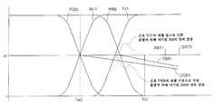
제5도는 제4도에 도시된 회로의 동작을 나타내는 파형도.5 is a waveform diagram showing the operation of the circuit shown in FIG.
제6도는 본 발명의 실시예 2의 동작을 나타내는 파형도.6 is a waveform diagram showing the operation of the second embodiment of the present invention;
* 도면의 주요부분에 대한 부호의 설명* Explanation of symbols for main parts of the drawings
WL1~WLn : 워드 라인WL1 ~ WLn: word line
DGT1 및 DGB1, ···, DGTm 및 DGBm : 디지트 라인쌍DGT1 and DGB1, DGTm and DGBm: Digit line pair
M11 및 M12 : N채널 트랜지스터 Vcc : 소스 전압M11 and M12: N-channel transistor Vcc: source voltage
RBT1 및 RBB1 : 판독 버스 라인 BS1 : 블록 선택 신호RBT1 and RBB1: read bus line BS1: block select signal
INV : 인버터 M13 : 등화 트랜지스터INV: Inverter M13: Equalization Transistor
AND1 : 논리적 회로 Y1D~YmD : 컬럼 선택 신호AND1: logical circuit Y1D ~ YmD: column select signal
SA1 : 센스 증폭기SA1: Sense Amplifier
[발명의 목적][Purpose of invention]
[발명이 속하는 기술분야 및 그 분야의 종래기술][Technical field to which the invention belongs and the prior art in that field]
본 발명은 반도체 메모리 디바이스에 관한 것으로, 구체적으로 디지트 라인 선택동안 판독 버스 라인 상의 전위가 변동되는 것을 방지하기 위한 회로를 가진 반도체 메모리 디바이스에 관한 것이다.The present invention relates to a semiconductor memory device, and more particularly to a semiconductor memory device having a circuit for preventing the potential on the read bus line from changing during digit line selection.
종래의 반도체 메모리 디바이스에 대하여 제1도를 참조하여 설명한다.A conventional semiconductor memory device will be described with reference to FIG.
제1도에서, WL1 내지 WLn은 워드 라인이고 DGT1 및 DBG1~DGTm 및 DBGm은 쌍으로 된 디지트 라인들이다. SRAM(스태틱 랜덤 액세스 메모리)의 메모리 셀들 MC11 내지 MCmm은 워드 라인과 쌍으로 된 디지트 라인들의 교점에 배열되어 메모리 셀 어레이를 구성한다.In FIG. 1, WL1 to WLn are word lines and DGT1 and DBG1 to DGTm and DBGm are paired digit lines. Memory cells MC11 to MCmm of the SRAM (static random access memory) are arranged at the intersections of the word lines and the paired digit lines to form a memory cell array.
M11 및 M12, ···, Mm1 및 Mm2는 서로 접속된 게이트들을 각각 갖고 있고 쌍으로 된 디지트 라인을 미리 충전시키기 위해서 소스 전압 Vcc를 쌍으로 된 디지트 라인 DGT1 및 DGB1, ···, DGTm 및 DGBm에 접속시키는데 적용되는 쌍으로 된 N채널 트랜지스터를 나타낸다. M13 내지 Mm3은 쌍으로 된 디지트 라인들 사이에 각각 접속되며 그 전위 레벨을 등화하는데 적용되는 쌍으로 된 N채널 트랜지스터 M11 및 M12, ···, Mm1 및 Mm2의 공통 접속부에 접속된 게이트를 가진 N채널 트랜지스터를 나타낸다.M11 and M12, Mm1 and Mm2 each have gates connected to each other and the digit lines DGT1 and DGB1 paired with the source voltage Vcc to precharge the paired digit lines, DGTm and DGBm. It shows a pair of N-channel transistors that are applied to connect to. M13 to Mm3 are connected between paired digit lines, respectively, and paired N-channel transistors M11 and M12, which are applied to equalize their potential levels, N with gates connected to the common connection of Mm1 and Mm2. Represents a channel transistor.
M14 및 M15, ···, Mm4 및 Mm5는 쌍으로 된 디지트 라인 DGT1 및 DGB1, ···, DGTm 및 DGBm과 판독 버스 라인 RBT1 및 RBB1 사이에 각각 접속되며 서로 접속된 게이트들을 가진 쌍으로 된 N채널 트랜지스터를 나타낸다.M14 and M15, Mm4 and Mm5 are paired N with paired digit lines DGT1 and DGB1, DGTm and DGBm and read bus lines RBT1 and RBB1, respectively, connected to each other Represents a channel transistor.
블록 선택 신호 BS1은 그의 출력이 단일 PDG인 인버터(1)로 입력된다. 단일 PDG는 쌍으로 된 N채널 사전 충전 트랜지스터 M11 및 M12, ···, Mm1 및 Mm2 및 동화 트랜지스터 M13 내지 Mm3의 게이트들의 공통 접속부로 공급된다.The block select signal BS1 is input to the
또한, 블록 선택 신호 BS1은 각 컬럼 선택 신호 Y1D 내지 YmD가 공급되는 다른 입력 단자를 가진 CMOS 논리적 회로 AND1 내지 ANDm의 하나의 입력 단자에 공급된다.Further, the block select signal BS1 is supplied to one input terminal of the CMOS logical circuits AND1 to ANDm having different input terminals to which the column select signals Y1D to YmD are supplied.
DMOS 논리적 회로 AND1 내지 ANDm의 출력신호 YJ1 내지 Yjm은 각각 쌍으로 된 N채널 트랜지스터 M14 및 M15, ···, Mm4 및 Mm5로 구성된 디지트 선택 스위치(이하,“YSW”라 한다)의 게이트 전극으로 공급된다.The output signals YJ1 to Yjm of the DMOS logical circuits AND1 to ANDm are supplied to the gate electrodes of the digit selector switches (hereinafter referred to as "YSWs") composed of paired N-channel transistors M14 and M15, ..., Mm4 and Mm5, respectively. do.
판독 버스 라인 RBT1 및 RBB1은 차동형 센스 증폭기 SA1에 접속된다.Read bus lines RBT1 and RBB1 are connected to differential sense amplifier SA1.
제1도중에서, SRAM의 판독 동작에 대해서 설명한다.In the first diagram, a read operation of the SRAM will be described.
임의의 블록이 비선택 상태에 있으면, 블록 선택 신호 BS1은 로우 레벨(L)이고, 사전 충전 N채널 트랜지스터 M11, M12 및 M13, ···, Mm1, Mm2 및 Mm3은 온 상태이다. 따라서, 쌍으로 된 디지트 라인 DGT1 및 DGB1, ···, DGTm 및 DGBm이 사전 충전된다.If any block is in the unselected state, the block select signal BS1 is at the low level (L), and the precharged N-channel transistors M11, M12 and M13, ..., Mm1, Mm2 and Mm3 are on. Thus, the paired digit lines DGT1 and DGB1, ..., DGTm and DGBm are precharged.
블록 선택 신호 BS1이 블록 선택 회로(도시 생략)에 의해서 선택되고, 블록을 선택 상태로 되게 하는 하이 레벨(H)로 되면, 워드 구동기(도시 생략)에 의해서 선택된 워드 라인 WL1상의 메모리 셀 MC11 내지 MClm의 전위가 각 메모리 셀들에 접속된 쌍으로 된 디지트 라인 DGT1 및 DGB1, ···, DGTm 및 DGBm으로 전달된다.When the block select signal BS1 is selected by the block select circuit (not shown) and reaches the high level H that causes the block to be selected, the memory cells MC11 to MClm on the word line WL1 selected by the word driver (not shown) are selected. The potential of is transferred to the paired digit lines DGT1 and DGB1, ..., DGTm and DGBm connected to the respective memory cells.
이어서, 컬럼 선택 신호 Y1D가 컬럼 선택 회로(도시 생략)에 의해서 선택되고 하이 레벨(H)로 될 때 논리적 회로 AND1이 선택되고 그의 출력 신호 Yj1이 하이 레벨(H)이 된다. 신호 Yj1이 N채널 트랜지스터 M14 및 M15가 턴온되며 선택된 디지트 라인 DGT1 및 DGB1의 전위가 판독 버스 라인 RBT1 및 RBB1로 각각 전달된다.Then, when the column select signal Y1D is selected by the column select circuit (not shown) and goes to the high level H, the logical circuit AND1 is selected and its output signal Yj1 becomes the high level H. N-channel transistors M14 and M15 are turned on with signal Yj1 and the potentials of selected digit lines DGT1 and DGB1 are transferred to read bus lines RBT1 and RBB1, respectively.
판독 버스 라인 RBT1과 RBB1간의 미소 전위차가 센스 증폭기(SA1)에 의해서 검출 및 증폭되어 데이터 판독이 행해진다.The small potential difference between the read bus lines RBT1 and RBB1 is detected and amplified by the sense amplifier SA1, and data reading is performed.
[발명이 이루고자 하는 기술적 과제][Technical problem to be achieved]
제2도는 리드 버스 라인 주변의 통상적인 회로를 상세하게 도시하고 있다. 제2도에는 제1도에 도시된 것과 동일한 구성 요소에는 동일한 참조 번호를 병기하였다.2 shows details of a typical circuit around a lead bus line. In FIG. 2, the same components as those shown in FIG. 1 are given the same reference numerals.
디지트 라인 선택 스위치(YSW) 및 쌍으로 된 디지트 라인을 구성하는 N채널 트랜지스터 M14 및 M15의 게이트간의 기생 용량을 각각 C11 및 C12로 표시하고, 게이트와 판독 버스 라인 RBT1 및 RBB1간의 기생 용량을 각각 C13 및 C14로 표시하면, 기생 용량 C11 및 C13 그리고 기생 용량 C12 및 C14는 N채널 트랜지스터 M14 및 M15 각각의 채널 폭 W에 비례한다.The parasitic capacitances between the gates of the N-channel transistors M14 and M15 constituting the digit line select switch (YSW) and the paired digit lines are denoted by C11 and C12, respectively, and the parasitic capacitances between the gate and the read bus lines RBT1 and RBB1 are denoted by C13, respectively. And C14, parasitic capacitances C11 and C13 and parasitic capacitances C12 and C14 are proportional to the channel width W of the N-channel transistors M14 and M15, respectively.
N채널 트랜지스터 M14 및 M15의 채널 길이는 이론적으로는 L이지만 제작 조건에 따라서 각각 L-α 및 L+α가 되고 메모리 셀 MC11에 기억된 데이터는“1”인 것으로 가정되었다.The channel lengths of the N-channel transistors M14 and M15 are theoretically L, but L-α and L + α, respectively, depending on fabrication conditions, and the data stored in the memory cell MC11 is assumed to be "1".
제3도는 제2도에 도시된 회로의 동작 파형을 나타내는 타이밍차트이다.3 is a timing chart showing an operation waveform of the circuit shown in FIG.
신호 PDG가 하이 레벨(H)일 때, 사전 충전 트랜지스터 M11 및 M12 및 등화 트랜지스터 M13은 온 상태가 되어 디지트 라인 DGT1 및 DGB1의 전위는 트랜지스터 M11 및 M12의 임계값만큼 소스 전압 Vcc 보다 낮은 Vr이 된다.When the signal PDG is at the high level (H), the precharge transistors M11 and M12 and the equalizing transistor M13 are turned on so that the potentials of the digit lines DGT1 and DGB1 become Vr lower than the source voltage Vcc by the thresholds of the transistors M11 and M12. .
이러한 상황에서는 신호 PDG의 상태가 H레벨에서 L레벨로 변화되어 쌍으로 된 디지트 라인 DGT1 및 DGB1상에 사전 충전 상태를 방출한다.In this situation, the state of the signal PDG is changed from H level to L level to release the precharge state on the paired digit lines DGT1 and DGB1.
그 후에, 워드 라인 WL1이 L레벨로부터 H레벨로 변화되고, 메모리 셀 MC11의 데이타가 쌍으로 된 디지트 라인 DGY1 및 DGB1상에서 판독된다. 이 경우에, 디지트 라인 DGB1의 전위는 L레벨로 낮아진다.Thereafter, word line WL1 is changed from L level to H level, and data of memory cell MC11 is read on paired digit lines DGY1 and DGB1. In this case, the potential of the digit line DGB1 is lowered to the L level.
디지트 라인 선택 스위치(YSW)를 구성하는 N채널 트랜지스터 M14 및 M15는 선택 신호 Yj1의 상태를 L레벨로부터 H레벨로 변경시킴에 의해서 턴온되어 디지트 라인 DGT1 및 DGB1상의 데이터를 판독 버스 라인 RBT1 및 RBB1로 전달한다.The N-channel transistors M14 and M15 constituting the digit line select switch YSW are turned on by changing the state of the select signal Yj1 from the L level to the H level to transfer data on the digit lines DGT1 and DGB1 to the read bus lines RBT1 and RBB1. To pass.
이때, N채널 트랜지스터 M14 및 M15의 게이트들과 디지트 라인 사이 그리고 트랜지스터 M14 및 M15의 기생 용량 C11 내지 C14로 인하여 게이트들과 판독 버스 라인들 사이에서 결합이 발생한다.At this time, coupling occurs between the gates of the N-channel transistors M14 and M15 and the digit line and between the gates and the read bus lines due to the parasitic capacitances C11 to C14 of the transistors M14 and M15.
디지트 라인 DGT1 및 DGB1 및 판독 버스 라인 RBT1 및 RBB1의 전위가 L레벨로부터 H레벨로의 선택 신호 Yj1의 상태 변화에 의해서 상승된다. 그러나, 디지트 라인 DGT1 및 DGB1과 그라운드(GND)간의 기생 용량이 실질적으로 기생 용량 C11 및 C12보다 크므로, 예를 들면 48배에 이르므로, 디지트 라인 DGT1 및 DGB1의 전위 라벨의 변동량은 매우 작다.The potentials of the digit lines DGT1 and DGB1 and the read bus lines RBT1 and RBB1 are raised by the state change of the selection signal Yj1 from the L level to the H level. However, since the parasitic capacitance between the digit lines DGT1 and DGB1 and ground (GND) is substantially larger than the parasitic capacitances C11 and C12, for example, up to 48 times, the variation in the potential labels of the digit lines DGT1 and DGB1 is very small.
그러나, 판독 버스 라인 RBT1 및 RBB1과 그라운드(GND)간의 기생 용량이 판독 버스 라인 RBT1 및 RBB1과 그라운드(GND)간의 기생 용량만큼 크지 않으므로, 판독 버스 라인 RBT1 및 RBB1 그리고 그라운드의 전위 레벨은 실질적으로 제3도에 도시한 바와 같이 상승된다.However, since the parasitic capacitance between read bus lines RBT1 and RBB1 and ground (GND) is not as large as the parasitic capacitance between read bus lines RBT1 and RBB1 and ground (GND), the potential levels of read bus lines RBT1 and RBB1 and ground are substantially zero. It is raised as shown in 3 degrees.
디지트 라인 선택 스위치(YSW)를 구성하는 N채널 트랜지스터 M14 및 M15가 턴온되면, 디지트 라인 DGT1 판독 버스 라인 RBT1의 전위 레벨에 등화되고, 디지트 라인 DGB1 및 판독 버스 라인 RBB1의 전위 레벨이 등화된다.When the N-channel transistors M14 and M15 constituting the digit line select switch YSW are turned on, they are equalized to the potential levels of the digit line DGT1 read bus line RBT1, and the potential levels of the digit line DGB1 and read bus line RBB1 are equalized.
상술한 바와 같이, 디지트 라인 선택 스위치(YSW)를 구성하는 N채널 트랜지스터 M14 및 M15가 불균형을 이룰 때, 트랜지스터 M14는 L-α의 채널 길이를 가진 트랜지스터 M14의 성능(채널 폭(W)/채널 길이(L)에 비례하는 전류 구동력)이 트랜지스터 M15의 성능보다 높기 때문에, 트랜지스터 M14에 의한 판독 버스 라인 RBB1의 전위 레벨의 하한 레이트보다 더 높은 레이트로 판독 버스 라인 RBT1 전위 레벨을 낮춘다. 이 동작은 메모리 셀 MC11에 기억된 데이터“l”의 판독 동작에 대한 역이며, 잘못된 판독이 원인일 수 있다. 또한, 판독 버스 라인 RBT1 과 RBB1간의 전위차를 센스 증폭기에 의해서 증폭되는 충분히 큰 값으로 증가시키는데 필요한 시간이 길어진다. 따라서, 판독 시간이 길어지는 문제가 발생한다.As described above, when the N-channel transistors M14 and M15 constituting the digit line select switch YSW are imbalanced, the transistor M14 performs the performance (channel width W / channel) of the transistor M14 with a channel length of L-α. Since the current driving force proportional to the length L) is higher than the performance of the transistor M15, the read bus line RBT1 potential level is lowered at a rate higher than the lower limit of the potential level of the read bus line RBB1 by the transistor M14. This operation is the inverse of the read operation of the data " l " stored in the memory cell MC11, and may be caused by an incorrect read. In addition, the time required to increase the potential difference between the read bus lines RBT1 and RBB1 to a sufficiently large value to be amplified by the sense amplifier becomes longer. Therefore, a problem arises in that the read time is long.
따라서, 본 발명의 목적은 디지트 라인을 선택하는데 있어서 발생되는 판독 버스 라인상의 전위 변동의 발생을 방지하고 판독 시간을 단축시킬 수 있는 반도체 메모리 디바이스를 제공하는 것이다.Accordingly, it is an object of the present invention to provide a semiconductor memory device capable of preventing the occurrence of potential fluctuations on the read bus line generated in selecting the digit line and reducing the read time.
본 발명에 따른 반도체 메모리 디바이스는 복수개의 비트 라인쌍, 상기 복수 개의 비트 라인 상에 접속된 복수개의 메모리 셀, 센스 증폭기, 상기 센스 증폭기에 접속된 판독 버스 라인쌍, 각 비트 라인쌍과 판독 버스 라인상간에 각각 제공된 제1 및 제2 트랜지스터, 상기 제1 및 제2트랜지스터의 게이트에 선택 신호를 공급하는 수단, 및 상기 판독 버스 라인쌍에 접속되어 상기 판독 버스 라인쌍를 사전 충전하여 등화하기 위해서 선택 신호의 역상의 신호에 응답하는 사전 충전 회로를 포함하며, 상기 사전 충전 회로는 복수개의 트랜지스터를 포함하며 상기 복수개의 트랜지스터의 게이트들과 판독 버스 라인쌍간의 기생 용량의 합은 제1 및 제2트랜지스터의 게이트들과 판독 버스 라인쌍들간의 기생 용량의 합과 같거나 이 합보다 큰 것을 특징으로 한다.The semiconductor memory device according to the present invention includes a plurality of bit line pairs, a plurality of memory cells connected on the plurality of bit lines, a sense amplifier, a read bus line pair connected to the sense amplifier, each bit line pair and a read bus line. Means for supplying a selection signal to the first and second transistors respectively provided between the phases, the gates of the first and second transistors, and a selection signal connected to the read bus line pair to precharge and equalize the read bus line pair A precharging circuit responsive to an inverse of the signal of the precharging circuit, the precharge circuit comprising a plurality of transistors, wherein the sum of parasitic capacitances between the gates of the plurality of transistors and the pair of read bus lines is determined by the first and second transistors. Is equal to or greater than the sum of the parasitic capacitances between the gates and the read bus line pairs. .
본 발명의 상술한 목적 및 다른 목적, 특징 및 이점은 이하에 첨부하는 도면들과 연계하여 취해진 본 발명의 상세한 설명을 참조할 때보다 자명하게 될 것이다.The above and other objects, features and advantages of the present invention will become more apparent when referring to the detailed description of the invention taken in conjunction with the accompanying drawings.
[발명의 구성 및 작용][Configuration and Function of Invention]
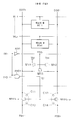
본 발명의 실시예 1를 제1도에 도시된 것과 동일한 구성 요소에 동일한 참조 번호를 부여한 제4도를 참조하여 설명한다.
제4도에서 WL1 내지 WLn은 워드 라인들이고 DGT1 및 DGB1, ···, DGTm 및 DGBm은 디지트 라인쌍을 나타낸다. SRAM의 메모리 셀 MC11 내지 MCnm은 워드 라인 및 디지트 라인의 교차점에 배열된다. N채널 트랜지스터 M11 및 M12는 소스 전압 Vcc와 디지트 라인 DGT1 및 DGB1 사이에 접속되며 디지트 라인을 서전 충전하는데 적용된다. N채널 트랜지스터 M13은 쌍으로 된 디지트 라인 DGT1과 DGB1 사이에 접속되며 이들 디지트 라인의 전위 레벨을 등화하는데 적용된다. 다른 디지트 라인쌍들은 동일한 구성을 갖는다.In Fig. 4, WL1 to WLn are word lines and DGT1 and DGB1, ..., DGTm and DGBm represent digit line pairs. Memory cells MC11 to MCnm of the SRAM are arranged at the intersections of word lines and digit lines. The N-channel transistors M11 and M12 are connected between the source voltage Vcc and the digit lines DGT1 and DGB1 and are applied to charge charge the digit line. The N-channel transistor M13 is connected between the paired digit lines DGT1 and DGB1 and is applied to equalize the potential levels of these digit lines. The other digit line pairs have the same configuration.
N채널 트랜지스터 M14 및 M15, ···, Mm4 및 Mm5는 쌍으로 된 디지트 라인 DGT1 및 DGB1, ···, DGTm 및 DGBm과 판독 버스 라인 RBT1 및 RBB1사이에 각각 접속된다. 블록 선택 신호 BS1은 인버터 INVl의 게이트에 입력되며 인버터 INVl로부터 출력된 신호 PDG는 쌍으로 된 N채널 사전 충전 트랜지스터 M11 및 M12 그리고 N채널 등화 트랜지스터 M13의 게이트들로 공급된다.The N-channel transistors M14 and M15, ..., Mm4 and Mm5 are connected between the paired digit lines DGT1 and DGB1, ..., DGTm and DGBm and the read bus lines RBT1 and RBB1, respectively. The block select signal BS1 is input to the gate of the inverter INVl and the signal PDG output from the inverter INVl is supplied to the gates of the paired N-channel precharge transistors M11 and M12 and the N-channel equalization transistor M13.
또한, 블록 선택 신호 BS1은 컬럼 선택 신호 Y1D가 공급되는 다른 입력 단자를 가진 CMOS 논리적 회로 AND1의 하나의 입력단자로 공급된다. CMOS 논리적 회로 AND1의 출력 신호는 인버터 INV3 및 INV4에 의해서 소정 시간만큼 지연되며, 디지트 라인 선택 스위치(YSW)를 구성하는 N채널 트랜지스터 M14 및 M15의 게이트로 입력되는 신호 Yj1이 된다.Further, the block select signal BS1 is supplied to one input terminal of the CMOS logical circuit AND1 having another input terminal to which the column select signal Y1D is supplied. The output signal of the CMOS logical circuit AND1 is delayed by the inverters INV3 and INV4 for a predetermined time, and becomes the signal Yj1 input to the gates of the N-channel transistors M14 and M15 constituting the digit line selection switch YSW.
N채널 트랜지스터 Ml6 및 Ml7은 소스 전압 Vcc와 판독 버스 라인 RBT1 및 RBB1 사이에 접속되며 판독 버스를 사전 충전하는데 적용된다. N채널 트랜지스터 Ml8은 판독 버스 라인 RBT1과 RBB1 사이에 접속되어 판독 버스 라인 RBT1 및 RBB1의 전위를 등화하는데 적용된다. 트랜지스터 Ml6, Ml7 및 Ml8은 전위 가변 방지 회로(10)를 구성한다.The N-channel transistors Ml6 and Ml7 are connected between the source voltage Vcc and the read bus lines RBT1 and RBB1 and are applied to precharge the read bus. The N-channel transistor Ml8 is connected between the read bus lines RBT1 and RBB1 and applied to equalize the potentials of the read bus lines RBT1 and RBB1. Transistors Ml6, Ml7, and Ml8 constitute a potential
블록 선택 신호 BS1은 인버터 INV2에 입력되며 인버터 INV2의 출력은 인버터 INV5 및 INV6을 지나서 결국 N채널 트랜지스터 Ml6, Ml7 및 Ml8의 게이트로 입력되는 신호 PRB가 된다.The block select signal BS1 is input to the inverter INV2, and the output of the inverter INV2 passes the inverters INV5 and INV6 and eventually becomes the signal PRB input to the gates of the N-channel transistors Ml6, Ml7 and Ml8.
N채널 트랜지스터 Ml6 및 Ml7의 게이트와 판독 버스 라인 RBT1 및 RBB1간의 기생 용량은 각각 Cl5 및 Cl6으로 되어 있고, N채널 트랜지스터 Ml8의 게이트와 판독 버스 라인 RBT1간의 기생 용량은 Cl7로 되어 있으며, N채널 트랜지스터 Ml8의 게이트와 판독 버스 라인 RBB1간의 기생 용량은 Cl8로 표시되어 있다.The parasitic capacitances between the gates of the N-channel transistors Ml6 and Ml7 and the read bus lines RBT1 and RBB1 are Cl5 and Cl6, respectively, and the parasitic capacitances between the gate and the read bus line RBT1 of the N-channel transistors Ml8 are Cl7. The parasitic capacitance between the gate of Ml8 and the read bus line RBB1 is denoted by Cl8.
N채널 트랜지스터 Ml6, Ml7 및 Ml8의 기생 용량은 다음 수학식 1이 성립하도록 결정된다.The parasitic capacitances of the N-channel transistors Ml6, Ml7 and Ml8 are determined so that the following equation (1) holds.
[수학식 1][Equation 1]
C13 + C14 = C15 + C16 + C17 + C18C13 + C14 = C15 + C16 + C17 + C18
여기서, C13 및 C14는 N채널 트랜지스터 M14 및 M15의 게이트와 판독 버스 라인 RBT1 및 RBB1간의 각 기생 용량이다.Here, C13 and C14 are parasitic capacitances between the gates of the N-channel transistors M14 and M15 and the read bus lines RBT1 and RBB1.
트랜지스터의 기생 용량을 제어하는 가장 간단한 방법은 그의 채널 길이(L) 혹은 채널 폭(W)을 제어하는 것이다. 이것은 트랜지스터의 제작과 관련하여 채널 길이를 일정하게 하는 것이 보다 바람직하므로, 그의 W의 값을 변화시켜 트랜지스터의 기생 용량을 제어하는 것이 바람직하다.The simplest way to control the parasitic capacitance of a transistor is to control its channel length (L) or channel width (W). It is more preferable to keep the channel length constant in relation to the fabrication of the transistor, and therefore, it is preferable to control the parasitic capacitance of the transistor by changing its value of W.
이 실시예에서는 다음 수학식에 따라 W의 값을 선택하므로써 수학식 1을 만족시킬 수 있다(트랜지스터 M14 및 M15의 W의 합 = 트랜지스터 Ml6 내지 Ml8의 W의 합).In this embodiment,
수학식 1은 C13 + C14 = Cl5 + Cl6 + Cl7 + Cl8로 표현될 수 있다.
따라서, 다음 수학식은 다음과 같이 성립된다.Therefore, the following equation is established as follows.
(트랜지스터 M14의 W) = (트랜지스터 Ml6 및 Ml8의 W의 합),(W of transistor M14) = (sum of W of transistors Ml6 and Ml8),
(트랜지스터 M15의 W) = (트랜지스터 Ml7 및 Ml8의 W의 합)(W of transistor M15) = (sum of W of transistors Ml7 and Ml8)
신호 PDG가 하이 레벨일 때, 사전 충전 트랜지스터 M11 및 M12 그리고 등화 트랜지스터 M13이 온 상태가 되므로, 디지트 라인 DGT1 및 DGB1의 전위는 트랜지스터 M11 및 M12의 임계값만큼 소스 전압 Vcc 보다 낮은 Vr이 된다. 이때, 판독 버스 라인을 사전 충전 및 등화하기 위한 제어 신호 PRB가 하이 레벨이므로, 판독 버스 라인 RBT1 및 RBB1을 사전 충전하기 위한 사전 충전 트랜지스터 Ml6 및 Ml7 및 등화 트랜지스터 Ml8은 턴온되고 판독 버스 라인 RBT1 및 RBB1의 전위는 트랜지스터 Ml6 혹은 Ml7의 임계값에 대응하는 전압만큼 소스 전압 Vcc보다 낮은 Vr이 된다.When the signal PDG is at the high level, the precharge transistors M11 and M12 and the equalizing transistor M13 are turned on, so that the potentials of the digit lines DGT1 and DGB1 become Vr lower than the source voltage Vcc by the thresholds of the transistors M11 and M12. At this time, since the control signal PRB for precharging and equalizing the read bus line is high level, the precharge transistors Ml6 and Ml7 and the equalizing transistor Ml8 for precharging the read bus lines RBT1 and RBB1 are turned on and the read bus lines RBT1 and RBB1 are turned on. The potential of becomes Vr lower than the source voltage Vcc by the voltage corresponding to the threshold of transistor Ml6 or Ml7.
이런 상황에서, 블록 선택 신호 BS1이 로우 레벨에서 하이 레벨로 변화될 때 신호 PDG의 상태는 H레벨에서 L레벨로 변화되고 N채널 트랜지스터 M11 및 M12는 턴오프되어 쌍으로 된 디지트 라인 DGT1 및 DGB1상의 사전 충전 상태를 해방시킨다.In this situation, when the block select signal BS1 is changed from low level to high level, the state of the signal PDG is changed from H level to L level, and the N-channel transistors M11 and M12 are turned off and on the paired digit lines DGT1 and DGB1. Free precharge.
따라서, 워드 라인 WL1은 L레벨에서 H레벨로 변화되고 메모리 셀 MC11의 데이터는 쌍으로 된 디지트 라인 DGT1 및 DGB1 상에서 판독된다. 이 경우에, 디지트 라인 DGT1의 전위는 L레벨로 낮아진다. 또한, 컬럼 선택 라인 Y1D는 도시하지 않은 컬럼 선택 회로에 의해서 하이 레벨이 된다.Thus, word line WL1 changes from L level to H level and data of memory cell MC11 is read on paired digit lines DGT1 and DGB1. In this case, the potential of the digit line DGT1 is lowered to the L level. In addition, the column select line Y1D is at a high level by a column select circuit not shown.
디지트 라인 DGT1 및 DGB1간의 전위차가 센스 증폭기에 의해서 증폭되는 큰 값으로 증가될 때 신호 PRB는 하이에서 로우 레벨로 변화되어 판독 버스 라인 RBT1 및 RBB1의 사전 충전 상태를 해방시킨다. 동시에, 디지트 라인 선택 스위치(YSW)를 구성하는 N채널 트랜지스터 M14 및 M15가 턴온 상태이므로, 선택 신호 Yj1은 로우에서 하이 레벨로 변화된다.When the potential difference between digit lines DGT1 and DGB1 increases to a large value that is amplified by the sense amplifier, the signal PRB changes from high to low level to release the precharge state of read bus lines RBT1 and RBB1. At the same time, since the N-channel transistors M14 and M15 constituting the digit line select switch YSW are turned on, the select signal Yj1 is changed from low to high level.
이 경우에, N채널 트랜지스터 M14 및 M15의 게이트와 디지트 라인간 그리고 트랜지스터 M14 및 M15의 기생 용량 C13 및 C14로 인한 게이트와 판독 버스 라인간에서 결합이 발생하여 판독 버스 라인 RBT1 및 RBB1의 전위 레벨이 증가되는 경향이 있다.In this case, a coupling occurs between the gate and the digit line of the N-channel transistors M14 and M15 and between the gate and the read bus line due to the parasitic capacitances C13 and C14 of the transistors M14 and M15 so that the potential levels of the read bus lines RBT1 and RBB1 are increased. There is a tendency to increase.
그러나, 로우로부터 하이로의 선택 신호 Yj1이 레벨 변화와 동시에 신호 PRB가 하이에서 로우로 변화되므로, 기생 용량 Cl5 내지 Cl8로 인하여 N채널 트랜지스터 Ml6, Ml7 및 Ml8의 게이트와 판독 버스 라인간에 결합이 생겨서 이로 인해서 판독 버스 라인의 레벨이 감소되는 경향이 있다.However, since the selection signal Yj1 from low to high changes from high to low at the same time as the level change, the parasitic capacitances Cl5 to Cl8 cause coupling between the gate and read bus lines of the N-channel transistors Ml6, Ml7 and Ml8. This tends to reduce the level of the read bus lines.
이 실시예에서는 판독 버스 라인의 결합에 원인을 제공하는 트랜지스터들의 기생 용량이 수학식 1에서 표시한 바와 같이 동일하게 되므로, 대향 결합에 의한 노이즈가 실질적으로 상쇄되어 판독 버스 라인의 전위의 실질적인 변화가 없게 된다.In this embodiment, since the parasitic capacitances of the transistors that contribute to the coupling of the read bus lines are the same as shown in
따라서, 디지트 라인 선택 스위치 YSW를 구성하는 N채널 트랜지스터 M14 및 M15의 채널 길이가 제4도에 도시한 바와 같이 변화될 때도 잘못된 데이터 판독은 발생되지 않는다.Therefore, even when the channel lengths of the N-channel transistors M14 and M15 constituting the digit line select switch YSW are changed as shown in FIG. 4, no erroneous data reading occurs.
이어서, 본 발명의 실시예 2에 대하여 설명한다. 실시예 2와 제1도에 도시된 실시예 1와의 차이점은 N채널 트랜지스터 Ml6 및 Ml7이 게이트와 판독 버스 라인 RBT1 및 RBB1간의 기생 용량 Cl5 및 Cl6, N채널 트랜지스터 Ml8의 게이트와 판독 버스 라인 RBT1간의 기생 용량 Cl7, 그리고 트랜지스터 Ml8이 게이트와 판독 버스 라인 RBB1간의 기생 용량 Cl8의 다음 수학식 2을 만족시킨다는 점이다.Next, Example 2 of this invention is described. Differences between Embodiment 2 and
[수학식 2][Equation 2]
C13 + C14
여기서, C13 및 C14는 N채널 트랜지스터 M14 및 M15의 게이트와 판독 버스 라인 RBT1 및 RBB1간의 기생 용량이다.Here, C13 and C14 are parasitic capacitances between the gates of the N-channel transistors M14 and M15 and the read bus lines RBT1 and RBB1.
수학식 2으로 표시된 N채널 트랜지스터의 기생 용량의 선택에 의해서, 디지트 라인 선택 스위치(YSW)의 선택 신호의 결합에 의해 발생되는 판독 버스 라인의 전위 변동량 보다 큰 전위 변동량을 동일한 판독 버스 라인에 제공할 수 있어서 디지트 라인의 전위보다도 판독 버스 라인의 전위를 낮게 할 수 있다.By selecting the parasitic capacitance of the N-channel transistor represented by Equation 2, a potential variation larger than that of the read bus line generated by the combination of the selection signals of the digit line select switch YSW can be provided to the same read bus line. In this way, the potential of the read bus line can be lower than that of the digit line.
제6도는 실시예 2의 동작에 대한 타이밍 차트이다. 제5도에 도시된 것의 일부분을 제외한 타이밍차트에 대하여 설명한다.6 is a timing chart for the operation of the second embodiment. A timing chart except for a part shown in FIG. 5 will be described.
신호 Yj1의 상태가 로우 레벨에서 하이 레벨로 변화될 때, 기생 용량 C13 및 C14로 인해서 N채널 트랜지스터 M14 및 M15의 게이트와 판독 버스 라인간에 신호 결합이 발생된다. 그러나, 신호 PRB의 상태가 하이 레벨로부터 로우 레벨로 변화 될 때 사전 충전 트랜지스터 Ml6 및 Ml7 및 등화 트랜지스터 Ml8의 게이트와 이들 트랜지스터의 기생 용량 Cl5 내지 Cl8로 인한 판독 버스 라인간에서 신호 결합이 발생하여 판독 버스 라인 RBT1 및 RBB1의 레벨이 낮게 된다.When the state of the signal Yj1 changes from low level to high level, signal coupling occurs between the gates of the N-channel transistors M14 and M15 and the read bus line due to the parasitic capacitances C13 and C14. However, when the state of the signal PRB changes from the high level to the low level, a signal coupling occurs between the gates of the precharge transistors Ml6 and Ml7 and the equalization transistor Ml8 and the read bus lines due to the parasitic capacitances Cl5 to Cl8 of these transistors to read them. The levels of bus lines RBT1 and RBB1 are low.
실시예 2에서는 판독 버스 라인의 전위를 낮게 하는 신호 결합의 원인이 되는 트랜지스터 Ml6 내지 Ml8의 기생 용량의 합이 트랜지스터 M14 및 M15이 기생 용량의 합보다 크게 선택되므로, 판독 버스 라인의 전위가 디지트 라인의 전위보다 낮은 (Vr-β)가 된다.In Embodiment 2, since the sum of the parasitic capacitances of the transistors Ml6 to Ml8, which causes the signal coupling to lower the potential of the read bus line, is selected so that the transistors M14 and M15 are larger than the sum of the parasitic capacitances, the potential of the read bus line is digit line. Becomes lower than the potential of (Vr-β).
기판과 N채널 트랜지스터 M14 및 M15의 소스간의 전위차가 보다 크고, 전류 구동력이, 디지트 라인 및 디지트 라인에 대응하는 판독 버스 라인의 전위들이 동일한 다음 수학식 3이 설정되어 있을 때 디지트 라인의 전위가 디지트 라인에 대응하는 판독 버스 라인의 전위보다 β만큼 큰 다음 수학식 4이 설정되어 있을 때보다 낮게 되므로, 센스 증폭기로 입력되는 판독 버스 라인간의 전위차는 실시예 1에서보다 높은 레이트로 크게 된다.The potential of the digit line is digit when the potential difference between the substrate and the sources of the N-channel transistors M14 and M15 is greater, and the current driving force is equal to the following equation (3) where the potentials of the read bus lines corresponding to the digit line and the digit line are set. Since the following equation 4, which is larger than the potential of the read bus line corresponding to the line, is lower than when the following equation (4) is set, the potential difference between the read bus lines input to the sense amplifier is increased at a higher rate than in the first embodiment.
[수학식 3][Equation 3]
DGT1 - RBT1 = 0, DGB1 - RBB1 = 0DGT1-RBT1 = 0, DGB1-RBB1 = 0
[수학식 4][Equation 4]
DGT1 - RBT1 = β, DGB1 - RBB1 = βDGT1-RBT1 = β, DGB1-RBB1 = β
그러나, 판독 버스 라인의 전위를 낮게 하는 결합이 종래 기술에서와 같이 너무 빈번할 때 잘못된 데이터 판독이 발생될 수 있으므로, 판독 버스 라인의 전위 감소가 제한된다.However, since a false data read can occur when the coupling that lowers the potential of the read bus line is too frequent as in the prior art, the potential reduction of the read bus line is limited.
따라서, N채널 트랜지스터의 전류 구동력의 향상으로 인한 동작 속도의 증가가, 제6도에 도시한 바와 같이 결합에 의한 전위 변동에 따른 동작 지연보다 클 때 실시예 1에 의해서 얻을 수 있는 것보다 고속의 동작이 가능하다. 즉 제6도에서, 판독 버스 라인 RBT1과 RBB1간의 전위차가 차동형 센스 증폭기에 의해서 증폭되는 충분히 큰 값이 되는 순시 시간 Tr3이 제5도에 도시된 순시 시간 Tr2보다 앞선다. 이에 대해서는 후술한다.Therefore, when the increase in the operating speed due to the improvement of the current driving force of the N-channel transistor is larger than that obtained by the first embodiment when the increase in the operating speed is larger than the operating delay due to the potential variation due to the coupling as shown in FIG. Operation is possible. That is, in FIG. 6, the instantaneous time Tr3, which is a sufficiently large value that the potential difference between the read bus lines RBT1 and RBB1 is amplified by the differential sense amplifier, precedes the instantaneous time Tr2 shown in FIG. This will be described later.
본 발명의 실시예 1에 의해서 실현되는 고속 동작의 장점 및 제작시의 장점에 대하여 종래 디바이스의 동작의 타이밍 차트를 나타내는 제3도 및 실시예 1의 타이밍차트를 나타내는 제5도를 참조하여 설명한다.The advantages of the high speed operation and the advantages in manufacturing attained by the first embodiment of the present invention will be described with reference to FIG. 3 showing a timing chart of the operation of the conventional device and FIG. 5 showing a timing chart of the first embodiment. .
제5도에서, Tw2는 워드 라인 WL1이 활성화되는 시간 순시점이고 Tr2는 판독 버스 라인 RBT1 및 RBB1간의 전위차가 차동 센스 증폭기에 의해서 증폭되는 충분히 큰 값이 되는 시간 순시점이다. 유사하게, 제3도에서 Tr5는 워드 라인이 활성화되는 시간 순시점이고 Tr5는 판독 버스 라인 RBT1 및 RBB1간의 전위차가 차동 센스 증폭기에 의해서 증폭되는 충분히 값이 되는 시간 순시점이다.In FIG. 5, Tw2 is a time instant at which word line WL1 is activated and Tr2 is a time instant at which the potential difference between read bus lines RBT1 and RBB1 is a sufficiently large value that is amplified by the differential sense amplifier. Similarly, in FIG. 3, Tr5 is the time instant at which the word line is activated and Tr5 is the time instant at which the potential difference between the read bus lines RBT1 and RBB1 is sufficiently high that it is amplified by the differential sense amplifier.
워드 라인 선택까지 종래 디바이스와 본 발명의 실시예 1의 동작이 동일한 회로 구성에 의해서 행해지므로, 다음 수학식 5이 성립한다.Since the operation of the conventional device and the first embodiment of the present invention are performed by the same circuit configuration until the word line selection, the following equation (5) holds.
[수학식 5][Equation 5]
Tw2 = Tw6Tw2 = Tw6
또한, 차동형 센스 증폭기에 의해서 증폭되는 충분히 큰 판독 버스 라인 RBT1 및 RBB1간의 전위차가 50mV라고 가정하면, 수학식 5는 제5도에 도시된 경우에서 다음 수학식 6으로 수정될 수 있다.Further, assuming that the potential difference between the sufficiently large read bus lines RBT1 and RBB1 amplified by the differential sense amplifier is 50 mV, Equation 5 can be modified to the following Equation 6 in the case shown in FIG.
[수학식 6][Equation 6]
RBT1 - RBB1 = 0 → 50mVRBT1-RBB1 = 0 → 50 mV
한편, 수학식 5은 제3도에 도시된 경우에서는 다음 수학식 7으로 수정된다.On the other hand, Equation 5 is modified to the following Equation 7 in the case shown in FIG.
[수학식 7][Equation 7]
RBT1 - RBB1 = 0 → -15mV → 0 → 50mVRBT1-RBB1 = 0 → -15mV → 0 → 50mV
따라서, 다음 수학식 8을 얻는다.Thus, the following expression (8) is obtained.
[수학식 8][Equation 8]
Tr2
수학식 5 및 수학식 8으로부터, 워드 라인의 전위가 증가되는 순시 시간점과 판독 버스 라인의 전위차가 차동형 센스 증폭기에 의해서 증폭되어 충분히 크게 되는 순시 시간점간의 차는 종래의 디바이스 및 실시예 1 양자에서 다음 수학식 9으로 표현될 수 있다.From equations (5) and (8), the difference between the instantaneous time point at which the potential of the word line is increased and the instantaneous time point at which the potential difference of the read bus line is amplified by the differential sense amplifier is sufficiently large, in both the conventional device and the first embodiment. It can be expressed by the following equation (9).
[수학식 9][Equation 9]
△Tr = Tr2 - Tr5ΔTr = Tr2-Tr5
시간차 △Tr이 1M 비트의 동기식 SRAM에 의해서 계산되었으므로, 궁극적으로 다음 수학식 10이 된다.Since the time difference [Delta] Tr is calculated by the 1M bit synchronous SRAM, the following
[수학식 10][Equation 10]
△Tr = 1.0nsΔTr = 1.0 ns
수학식 10으로부터, 본 발명이 비동기식 동작을 행하는데 사용될 경우 액세스 시간 1.0ns 만큼 단축되고, 본 발명이 동기식 동작을 행하는데 사용될 경우에는 사이클 타이밍이 1.0ns 만큼 단축되는 장점이 얻어지는 것은 자명하다.From
기술된 실시예에 따르면 트랜지스터들의 채널 폭 W에 의해서 기생 용량이 제어되지만, 트랜지스터의 채널 길이 L 에 의해서 기생 용량을 제어하는 것이 가능하다.According to the described embodiment the parasitic capacitance is controlled by the channel width W of the transistors, but it is possible to control the parasitic capacitance by the channel length L of the transistor.
이제까지, 특정한 실시예와 관련하여 본 발명을 설명하였지만, 이러한 설명이 제한적인 의미로서 해석되어서는 안된다. 본 발명의 설명을 참조할 때 본 기술 분야에 숙력된 자에게 개시된 실시예의 다양한 변화가 가능함은 자명하다. 따라서 첨부된 청구 범위는 본 발명의 영역 내에 속하는 임의의 변경 혹은 실시예를 커버하려고 생각하고 있다.While the invention has been described with reference to specific embodiments so far, this description should not be interpreted in a limiting sense. When referring to the description of the present invention, it will be apparent that various changes in the embodiments disclosed to those skilled in the art are possible. Accordingly, the appended claims are intended to cover any changes or embodiments falling within the scope of the invention.
Claims (9)
Applications Claiming Priority (2)
| Application Number | Priority Date | Filing Date | Title |
|---|---|---|---|
| JP14831296A JP3230435B2 (en) | 1996-05-17 | 1996-05-17 | Semiconductor storage device |
| JP96-148312 | 1996-05-17 |
Publications (2)
| Publication Number | Publication Date |
|---|---|
| KR970076851A KR970076851A (en) | 1997-12-12 |
| KR100242516B1 true KR100242516B1 (en) | 2000-02-01 |
Family
ID=15449982
Family Applications (1)
| Application Number | Title | Priority Date | Filing Date |
|---|---|---|---|
| KR1019970019157A Expired - Fee Related KR100242516B1 (en) | 1996-05-17 | 1997-05-17 | Semiconductor memory device with function to prevent potential fluctuations in read buses due to coupling |
Country Status (3)
| Country | Link |
|---|---|
| US (1) | US5742545A (en) |
| JP (1) | JP3230435B2 (en) |
| KR (1) | KR100242516B1 (en) |
Cited By (1)
| Publication number | Priority date | Publication date | Assignee | Title |
|---|---|---|---|---|
| KR100355227B1 (en) * | 2000-01-06 | 2002-10-11 | 삼성전자 주식회사 | Data receiver |
Families Citing this family (4)
| Publication number | Priority date | Publication date | Assignee | Title |
|---|---|---|---|---|
| JP3085241B2 (en) * | 1997-04-11 | 2000-09-04 | 日本電気株式会社 | Semiconductor storage device |
| US6172920B1 (en) * | 2000-02-04 | 2001-01-09 | International Business Machines Corporation | Data transfer using two-stage bit switch in memory circuit |
| KR100510737B1 (en) * | 2002-06-29 | 2005-08-30 | 매그나칩 반도체 유한회사 | semiconductor memory device |
| JP5137178B2 (en) * | 2007-02-19 | 2013-02-06 | ルネサスエレクトロニクス株式会社 | Semiconductor integrated circuit device and layout method thereof |
Family Cites Families (5)
| Publication number | Priority date | Publication date | Assignee | Title |
|---|---|---|---|---|
| JP2667946B2 (en) * | 1992-09-21 | 1997-10-27 | 三菱電機株式会社 | Semiconductor storage device |
| JP2812097B2 (en) * | 1992-09-30 | 1998-10-15 | 日本電気株式会社 | Semiconductor storage device |
| JP2937719B2 (en) * | 1993-12-10 | 1999-08-23 | 株式会社東芝 | Semiconductor storage device |
| KR960009956B1 (en) * | 1994-02-16 | 1996-07-25 | 현대전자산업 주식회사 | Sense Amplifiers in Semiconductor Devices |
| DE69621293T2 (en) * | 1995-08-02 | 2002-12-12 | Matsushita Electric Industrial Co., Ltd. | Ferroelectric storage device |
-
1996
- 1996-05-17 JP JP14831296A patent/JP3230435B2/en not_active Expired - Fee Related
-
1997
- 1997-05-14 US US08/854,450 patent/US5742545A/en not_active Expired - Fee Related
- 1997-05-17 KR KR1019970019157A patent/KR100242516B1/en not_active Expired - Fee Related
Cited By (1)
| Publication number | Priority date | Publication date | Assignee | Title |
|---|---|---|---|---|
| KR100355227B1 (en) * | 2000-01-06 | 2002-10-11 | 삼성전자 주식회사 | Data receiver |
Also Published As
| Publication number | Publication date |
|---|---|
| US5742545A (en) | 1998-04-21 |
| JP3230435B2 (en) | 2001-11-19 |
| JPH09306173A (en) | 1997-11-28 |
| KR970076851A (en) | 1997-12-12 |
Similar Documents
| Publication | Publication Date | Title |
|---|---|---|
| US4417328A (en) | Random access semiconductor memory device using MOS transistors | |
| EP0398245B1 (en) | Dynamic type random-access memory | |
| US4397000A (en) | Output circuit | |
| US6225834B1 (en) | Bit line sense amplifier | |
| JPH0612632B2 (en) | Memory circuit | |
| JPH0422318B2 (en) | ||
| US4656608A (en) | Semiconductor memory device | |
| US5508643A (en) | Bitline level insensitive sense amplifier | |
| JPH06162776A (en) | Semiconductor memory circuit | |
| EP0458351A2 (en) | Semiconductor memory circuit | |
| EP0398244A2 (en) | Dynamic type random-acces memory | |
| US4131951A (en) | High speed complementary MOS memory | |
| US4433393A (en) | Semiconductor memory device | |
| EP0827151B1 (en) | Self cut-off type sense amplifier operable over a wide range of power supply voltages | |
| JPS6362839B2 (en) | ||
| US5295104A (en) | Integrated circuit with precharged internal data bus | |
| KR910004733B1 (en) | Semiconductor memory device having data bus reset circuit | |
| EP0420189A2 (en) | Sense amplifier circuit | |
| US5777934A (en) | Semiconductor memory device with variable plate voltage generator | |
| US6067264A (en) | High speed semiconductor memory device | |
| US5646892A (en) | Data reading circuit | |
| US5257226A (en) | Integrated circuit with self-biased differential data lines | |
| US6421289B1 (en) | Method and apparatus for charge-transfer pre-sensing | |
| US5742545A (en) | Semiconductor memory device having function of preventing potential variation of read bus due to coupling | |
| EP0547892A2 (en) | An integrated circuit with self-biased differential data lines |
Legal Events
| Date | Code | Title | Description |
|---|---|---|---|
| A201 | Request for examination | ||
| PA0109 | Patent application |
St.27 status event code: A-0-1-A10-A12-nap-PA0109 |
|
| PA0201 | Request for examination |
St.27 status event code: A-1-2-D10-D11-exm-PA0201 |
|
| R17-X000 | Change to representative recorded |
St.27 status event code: A-3-3-R10-R17-oth-X000 |
|
| PG1501 | Laying open of application |
St.27 status event code: A-1-1-Q10-Q12-nap-PG1501 |
|
| E701 | Decision to grant or registration of patent right | ||
| PE0701 | Decision of registration |
St.27 status event code: A-1-2-D10-D22-exm-PE0701 |
|
| GRNT | Written decision to grant | ||
| PR0701 | Registration of establishment |
St.27 status event code: A-2-4-F10-F11-exm-PR0701 |
|
| PR1002 | Payment of registration fee |
St.27 status event code: A-2-2-U10-U11-oth-PR1002 Fee payment year number: 1 |
|
| PG1601 | Publication of registration |
St.27 status event code: A-4-4-Q10-Q13-nap-PG1601 |
|
| FPAY | Annual fee payment |
Payment date: 20021025 Year of fee payment: 4 |
|
| PR1001 | Payment of annual fee |
St.27 status event code: A-4-4-U10-U11-oth-PR1001 Fee payment year number: 4 |
|
| PN2301 | Change of applicant |
St.27 status event code: A-5-5-R10-R11-asn-PN2301 |
|
| PN2301 | Change of applicant |
St.27 status event code: A-5-5-R10-R14-asn-PN2301 |
|
| PN2301 | Change of applicant |
St.27 status event code: A-5-5-R10-R13-asn-PN2301 St.27 status event code: A-5-5-R10-R11-asn-PN2301 |
|
| LAPS | Lapse due to unpaid annual fee | ||
| PC1903 | Unpaid annual fee |
St.27 status event code: A-4-4-U10-U13-oth-PC1903 Not in force date: 20031111 Payment event data comment text: Termination Category : DEFAULT_OF_REGISTRATION_FEE |
|
| PC1903 | Unpaid annual fee |
St.27 status event code: N-4-6-H10-H13-oth-PC1903 Ip right cessation event data comment text: Termination Category : DEFAULT_OF_REGISTRATION_FEE Not in force date: 20031111 |