KR100262003B1 - 반도체 메모리 - Google Patents
반도체 메모리 Download PDFInfo
- Publication number
- KR100262003B1 KR100262003B1 KR1019970072218A KR19970072218A KR100262003B1 KR 100262003 B1 KR100262003 B1 KR 100262003B1 KR 1019970072218 A KR1019970072218 A KR 1019970072218A KR 19970072218 A KR19970072218 A KR 19970072218A KR 100262003 B1 KR100262003 B1 KR 100262003B1
- Authority
- KR
- South Korea
- Prior art keywords
- memory cell
- switching means
- bit lines
- cell matrix
- semiconductor memory
- Prior art date
- Legal status (The legal status is an assumption and is not a legal conclusion. Google has not performed a legal analysis and makes no representation as to the accuracy of the status listed.)
- Expired - Fee Related
Links
Images


Classifications
-
- G—PHYSICS
- G11—INFORMATION STORAGE
- G11C—STATIC STORES
- G11C7/00—Arrangements for writing information into, or reading information out from, a digital store
- G11C7/10—Input/output [I/O] data interface arrangements, e.g. I/O data control circuits, I/O data buffers
- G11C7/1048—Data bus control circuits, e.g. precharging, presetting, equalising
-
- G—PHYSICS
- G11—INFORMATION STORAGE
- G11C—STATIC STORES
- G11C29/00—Checking stores for correct operation ; Subsequent repair; Testing stores during standby or offline operation
- G11C29/04—Detection or location of defective memory elements, e.g. cell constructio details, timing of test signals
- G11C29/08—Functional testing, e.g. testing during refresh, power-on self testing [POST] or distributed testing
- G11C29/12—Built-in arrangements for testing, e.g. built-in self testing [BIST] or interconnection details
- G11C29/1201—Built-in arrangements for testing, e.g. built-in self testing [BIST] or interconnection details comprising I/O circuitry
-
- G—PHYSICS
- G11—INFORMATION STORAGE
- G11C—STATIC STORES
- G11C29/00—Checking stores for correct operation ; Subsequent repair; Testing stores during standby or offline operation
- G11C29/04—Detection or location of defective memory elements, e.g. cell constructio details, timing of test signals
- G11C29/08—Functional testing, e.g. testing during refresh, power-on self testing [POST] or distributed testing
- G11C29/12—Built-in arrangements for testing, e.g. built-in self testing [BIST] or interconnection details
- G11C29/14—Implementation of control logic, e.g. test mode decoders
-
- G—PHYSICS
- G11—INFORMATION STORAGE
- G11C—STATIC STORES
- G11C7/00—Arrangements for writing information into, or reading information out from, a digital store
- G11C7/12—Bit line control circuits, e.g. drivers, boosters, pull-up circuits, pull-down circuits, precharging circuits, equalising circuits, for bit lines
Landscapes
- For Increasing The Reliability Of Semiconductor Memories (AREA)
- Dram (AREA)
Abstract
Description
Claims (3)
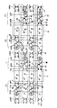
- 공통 데이타 입출력라인을 갖는 반도체 메모리에 있어서,워드라인에 의해 구동되고 비트라인을 통하여 데이타가 입력 또는 출력되는 다수개의 메모리 셀을 구비하고, 상기 비트라인을 상호 공유하는 이웃한 두 개의 메모리 셀 매트릭스와;제 1 제어신호에 의해 제어되어 상기 이웃한 두 개의 메모리 셀 매트릭스 사이에서 상기 비트라인을 전기적으로 연결하거나 단절시키는 제 1 스위칭 수단과;제 2 제어신호에 의해 제어되어 상기 이웃한 두 개의 메모리 셀 가운데 하나의 메모리 셀 매트릭스와 제 1 스위칭 수단 사이에 연결되어 상기 비트라인을 전기적으로 연결하거나 단절시키는 제 2 스위칭 수단과;제 3 제어신호에 의해 제어되어 상기 제 1 스위칭 수단과 상기 제 2 스위칭 수단 사이에 연결되는 비트라인과 상기 공통 데이타 입출력라인을 전기적으로 연결하거나 단절시키는 제 3 스위칭 수단을 포함하는 반도체 메모리.
- 청구항 1에 있어서, 상기 각각의 메모리 셀 매트릭스의 비트라인 가운데 동일한 컬럼어드레스로 지정된 비트라인이 상기 제 1 스위칭 수단에 의해 전기적으로 연결되거나 단절되는 것이 특징인 반도체 메모리.
- 청구항 1에 있어서, 상기 제 1 스위칭 수단은 상기 반도체 메모리의 테스트 동작시에 턴 온되는 것이 특징인 반도체 메모리.
Priority Applications (1)
| Application Number | Priority Date | Filing Date | Title |
|---|---|---|---|
| KR1019970072218A KR100262003B1 (ko) | 1997-12-23 | 1997-12-23 | 반도체 메모리 |
Applications Claiming Priority (1)
| Application Number | Priority Date | Filing Date | Title |
|---|---|---|---|
| KR1019970072218A KR100262003B1 (ko) | 1997-12-23 | 1997-12-23 | 반도체 메모리 |
Publications (2)
| Publication Number | Publication Date |
|---|---|
| KR19990052687A KR19990052687A (ko) | 1999-07-15 |
| KR100262003B1 true KR100262003B1 (ko) | 2000-07-15 |
Family
ID=19528245
Family Applications (1)
| Application Number | Title | Priority Date | Filing Date |
|---|---|---|---|
| KR1019970072218A Expired - Fee Related KR100262003B1 (ko) | 1997-12-23 | 1997-12-23 | 반도체 메모리 |
Country Status (1)
| Country | Link |
|---|---|
| KR (1) | KR100262003B1 (ko) |
Cited By (1)
| Publication number | Priority date | Publication date | Assignee | Title |
|---|---|---|---|---|
| US8363498B2 (en) | 2010-05-27 | 2013-01-29 | Hynix Semiconductor Inc. | Non-volatile memory device |
Families Citing this family (2)
| Publication number | Priority date | Publication date | Assignee | Title |
|---|---|---|---|---|
| KR100627515B1 (ko) * | 2004-10-04 | 2006-09-21 | 주식회사 하이닉스반도체 | 메모리 장치 및 그의 테스트 방법 |
| KR101005152B1 (ko) * | 2004-11-22 | 2011-01-04 | 주식회사 하이닉스반도체 | 반도체 메모리 소자의 데이터 입출력 라인을 공유하는방법 및 장치 |
-
1997
- 1997-12-23 KR KR1019970072218A patent/KR100262003B1/ko not_active Expired - Fee Related
Cited By (1)
| Publication number | Priority date | Publication date | Assignee | Title |
|---|---|---|---|---|
| US8363498B2 (en) | 2010-05-27 | 2013-01-29 | Hynix Semiconductor Inc. | Non-volatile memory device |
Also Published As
| Publication number | Publication date |
|---|---|
| KR19990052687A (ko) | 1999-07-15 |
Similar Documents
| Publication | Publication Date | Title |
|---|---|---|
| KR960001778B1 (ko) | 이중포트메모리 및 그 데이터 전송방법 | |
| KR970017611A (ko) | 다수의 메모리 어레이내에 분포된 다수의 뱅크들을 갖는 동기성 반도체 메모리 장치 | |
| KR840003894A (ko) | 반도체 기억장치 | |
| KR970029841A (ko) | 감소 칩 영역을 가진 반도체 메모리 소자 | |
| KR920013475A (ko) | 용장 기억 소자를 포함하는 메모리를 가진 집적회로 및 메모리의 동작 방법 | |
| KR100390615B1 (ko) | 반도체 메모리 장치 | |
| KR0164391B1 (ko) | 고속동작을 위한 회로 배치 구조를 가지는 반도체 메모리 장치 | |
| KR880003326A (ko) | 다방향 데이타 억세서 가능 반도체 메모리 장치 | |
| EP0361561B1 (en) | Integrated memory circuit comprising a parallel and serial input and output | |
| KR100262003B1 (ko) | 반도체 메모리 | |
| KR940006264A (ko) | 반도체 메모리 회로 | |
| JPH05342855A (ja) | 半導体メモリ回路 | |
| EP0276852B1 (en) | Random access memory device with nibble mode operation | |
| WO2003075280B1 (en) | Semiconductor storing device | |
| KR970023432A (ko) | 신속한 랜덤 액세스를 위한 반도체 메모리 소자 | |
| US6628536B2 (en) | Semiconductor memory device | |
| US5544093A (en) | Dual port multiple block memory capable of time divisional operation | |
| US5495443A (en) | Dynamic memory having a ground control circuit | |
| US7663936B2 (en) | Memory circuit and semiconductor device including the memory circuit, the memory circuit including selectors for selecting a data holding circuit | |
| KR100195671B1 (ko) | 반도체 메모리 장치 | |
| KR100267132B1 (ko) | 반도체 기억장치 | |
| US5359567A (en) | Semiconductor memory device | |
| US5479373A (en) | Semiconductor memory device having a plurality of blocks | |
| WO2002101748A2 (en) | Sense amplifier and architecture for open digit arrays | |
| US6333868B1 (en) | Semiconductor memory device having selectively shielded data lines |
Legal Events
| Date | Code | Title | Description |
|---|---|---|---|
| A201 | Request for examination | ||
| PA0109 | Patent application |
St.27 status event code: A-0-1-A10-A12-nap-PA0109 |
|
| PA0201 | Request for examination |
St.27 status event code: A-1-2-D10-D11-exm-PA0201 |
|
| R17-X000 | Change to representative recorded |
St.27 status event code: A-3-3-R10-R17-oth-X000 |
|
| PG1501 | Laying open of application |
St.27 status event code: A-1-1-Q10-Q12-nap-PG1501 |
|
| PN2301 | Change of applicant |
St.27 status event code: A-3-3-R10-R13-asn-PN2301 St.27 status event code: A-3-3-R10-R11-asn-PN2301 |
|
| E701 | Decision to grant or registration of patent right | ||
| PE0701 | Decision of registration |
St.27 status event code: A-1-2-D10-D22-exm-PE0701 |
|
| GRNT | Written decision to grant | ||
| PR0701 | Registration of establishment |
St.27 status event code: A-2-4-F10-F11-exm-PR0701 |
|
| PR1002 | Payment of registration fee |
St.27 status event code: A-2-2-U10-U11-oth-PR1002 Fee payment year number: 1 |
|
| PG1601 | Publication of registration |
St.27 status event code: A-4-4-Q10-Q13-nap-PG1601 |
|
| PR1001 | Payment of annual fee |
St.27 status event code: A-4-4-U10-U11-oth-PR1001 Fee payment year number: 4 |
|
| PR1001 | Payment of annual fee |
St.27 status event code: A-4-4-U10-U11-oth-PR1001 Fee payment year number: 5 |
|
| PR1001 | Payment of annual fee |
St.27 status event code: A-4-4-U10-U11-oth-PR1001 Fee payment year number: 6 |
|
| PR1001 | Payment of annual fee |
St.27 status event code: A-4-4-U10-U11-oth-PR1001 Fee payment year number: 7 |
|
| PR1001 | Payment of annual fee |
St.27 status event code: A-4-4-U10-U11-oth-PR1001 Fee payment year number: 8 |
|
| PR1001 | Payment of annual fee |
St.27 status event code: A-4-4-U10-U11-oth-PR1001 Fee payment year number: 9 |
|
| PR1001 | Payment of annual fee |
St.27 status event code: A-4-4-U10-U11-oth-PR1001 Fee payment year number: 10 |
|
| PR1001 | Payment of annual fee |
St.27 status event code: A-4-4-U10-U11-oth-PR1001 Fee payment year number: 11 |
|
| FPAY | Annual fee payment |
Payment date: 20110325 Year of fee payment: 12 |
|
| PR1001 | Payment of annual fee |
St.27 status event code: A-4-4-U10-U11-oth-PR1001 Fee payment year number: 12 |
|
| LAPS | Lapse due to unpaid annual fee | ||
| PC1903 | Unpaid annual fee |
St.27 status event code: A-4-4-U10-U13-oth-PC1903 Not in force date: 20120426 Payment event data comment text: Termination Category : DEFAULT_OF_REGISTRATION_FEE |
|
| PC1903 | Unpaid annual fee |
St.27 status event code: N-4-6-H10-H13-oth-PC1903 Ip right cessation event data comment text: Termination Category : DEFAULT_OF_REGISTRATION_FEE Not in force date: 20120426 |
|
| P22-X000 | Classification modified |
St.27 status event code: A-4-4-P10-P22-nap-X000 |