KR100299563B1 - 반도체 소자의 캐패시터 제조방법 - Google Patents
반도체 소자의 캐패시터 제조방법 Download PDFInfo
- Publication number
- KR100299563B1 KR100299563B1 KR1019970028698A KR19970028698A KR100299563B1 KR 100299563 B1 KR100299563 B1 KR 100299563B1 KR 1019970028698 A KR1019970028698 A KR 1019970028698A KR 19970028698 A KR19970028698 A KR 19970028698A KR 100299563 B1 KR100299563 B1 KR 100299563B1
- Authority
- KR
- South Korea
- Prior art keywords
- thin film
- film
- pzt thin
- forming
- capacitor
- Prior art date
- Legal status (The legal status is an assumption and is not a legal conclusion. Google has not performed a legal analysis and makes no representation as to the accuracy of the status listed.)
- Expired - Fee Related
Links
Images


Classifications
-
- H—ELECTRICITY
- H10—SEMICONDUCTOR DEVICES; ELECTRIC SOLID-STATE DEVICES NOT OTHERWISE PROVIDED FOR
- H10D—INORGANIC ELECTRIC SEMICONDUCTOR DEVICES
- H10D1/00—Resistors, capacitors or inductors
- H10D1/60—Capacitors
- H10D1/68—Capacitors having no potential barriers
- H10D1/682—Capacitors having no potential barriers having dielectrics comprising perovskite structures
-
- H—ELECTRICITY
- H10—SEMICONDUCTOR DEVICES; ELECTRIC SOLID-STATE DEVICES NOT OTHERWISE PROVIDED FOR
- H10D—INORGANIC ELECTRIC SEMICONDUCTOR DEVICES
- H10D1/00—Resistors, capacitors or inductors
- H10D1/60—Capacitors
- H10D1/68—Capacitors having no potential barriers
- H10D1/692—Electrodes
- H10D1/694—Electrodes comprising noble metals or noble metal oxides
Landscapes
- Semiconductor Memories (AREA)
Abstract
Description
Claims (6)
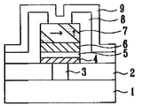
- 하부기판상에 형성된 절연막의 소정부위에 하부기판과 캐패시터 사이의 수직배선 형성을 위한 콘택홀을 형성하는 단계와, 상기 콘택홀 내에 다결정실리콘을 증착하여 배선 플러그를 형성하는 단계와, 상기 배선 플러그를 포함한 절연막상에 금속확산 방지막, Pt 하부전극 및 소정 두께의 강유전성 PZT 박막을 순차적으로 형성하는 단계와, 상기 PZT 박막의 미세구조를 하부기판의 수직방향보다 수평방향으로 배향성을 갖는 입자를 더 많이 가진 PZT 박막으로 변경시키는 단계와, 상기 강유전성 PZT 박막 상부에 규소 산화막을 소정 두께로 증착하는 단계와, 포토 마스크 및 건식식각 공정을 통해 상기 규소 산화막을 부분식각하여 상기 PZT 박막의 상부면을 노출시키는 단계와, 전체구조 상부에 상부적극을 형성하는 단계로 이루어짐을 특징으로 하는 반도체 소자의 캐패시터 형성방법.
- 제1항에 있어서, 상기 금속확산 방지막으로 Ti/TiN 막을 사용하고 그 두께는 300-3000Å으로 하는 것을 특징으로 하는 반도체 소자의 캐패시터 형성방법.
- 제1항에 있어서, 상기 금속확산 방지막으로 Ta/TaN 막을 사용하고, 그 두께는 300-3000Å으로 하는 것을 특징으로 하는 반도체 소자의 캐패시터 형성방법.
- 제1항에 있어서, 상기 금속확산 방지막으로 Ti/TiSiN 막 또는 Ta/TaSiN 막을 사용하고, 그 두께는 300-3000Å으로 하는 것을 특징으로 하는 반도체 소자의 캐패시터 형성방법.
- 제1항에 있어서, 상기 PZT 박막 형성시 100-1000Å으로 전면 증착하는 것을 특징으로 하는 반도체 소자의 캐패시터 형성방법.
- 제1항에 있어서, 상기 강유전성 PZT 박막을 형성한 직후 냉각전에 RF 플라즈마를 끄고 그 온도구간에서 5-20분간 열처리를 하고, 분당 30℃ 이내로 냉각하여 PZT 박막의 미세구조를 기판의 수평방향으로 배향성을 갖는 입자를 가진 PZT 박막으로 변경하는 것을 특징으로 하는 반도체 소자의 캐패시터 형성방법.
Priority Applications (2)
| Application Number | Priority Date | Filing Date | Title |
|---|---|---|---|
| KR1019970028698A KR100299563B1 (ko) | 1997-06-28 | 1997-06-28 | 반도체 소자의 캐패시터 제조방법 |
| US09/105,278 US6162698A (en) | 1997-06-28 | 1998-06-26 | Method of manufacturing a capacitor in a semiconductor device |
Applications Claiming Priority (1)
| Application Number | Priority Date | Filing Date | Title |
|---|---|---|---|
| KR1019970028698A KR100299563B1 (ko) | 1997-06-28 | 1997-06-28 | 반도체 소자의 캐패시터 제조방법 |
Publications (2)
| Publication Number | Publication Date |
|---|---|
| KR19990004571A KR19990004571A (ko) | 1999-01-15 |
| KR100299563B1 true KR100299563B1 (ko) | 2001-11-22 |
Family
ID=37528738
Family Applications (1)
| Application Number | Title | Priority Date | Filing Date |
|---|---|---|---|
| KR1019970028698A Expired - Fee Related KR100299563B1 (ko) | 1997-06-28 | 1997-06-28 | 반도체 소자의 캐패시터 제조방법 |
Country Status (1)
| Country | Link |
|---|---|
| KR (1) | KR100299563B1 (ko) |
Citations (2)
| Publication number | Priority date | Publication date | Assignee | Title |
|---|---|---|---|---|
| JPH0778943A (ja) * | 1993-09-06 | 1995-03-20 | Tdk Corp | 不揮発性メモリ |
| JPH08139307A (ja) * | 1994-11-02 | 1996-05-31 | Toyota Central Res & Dev Lab Inc | 強誘電体薄膜形成用電極 |
-
1997
- 1997-06-28 KR KR1019970028698A patent/KR100299563B1/ko not_active Expired - Fee Related
Patent Citations (2)
| Publication number | Priority date | Publication date | Assignee | Title |
|---|---|---|---|---|
| JPH0778943A (ja) * | 1993-09-06 | 1995-03-20 | Tdk Corp | 不揮発性メモリ |
| JPH08139307A (ja) * | 1994-11-02 | 1996-05-31 | Toyota Central Res & Dev Lab Inc | 強誘電体薄膜形成用電極 |
Also Published As
| Publication number | Publication date |
|---|---|
| KR19990004571A (ko) | 1999-01-15 |
Similar Documents
| Publication | Publication Date | Title |
|---|---|---|
| US5573979A (en) | Sloped storage node for a 3-D dram cell structure | |
| US6338994B1 (en) | Semiconductor device and method of fabricating thereof | |
| US6211542B1 (en) | Completely encapsulated top electrode of a ferroelectric capacitor using a lead-enhanced escapsulation layer | |
| US6096592A (en) | Methods of forming integrated circuit capacitors having plasma treated regions therein | |
| US6432767B2 (en) | Method of fabricating semiconductor device | |
| KR100390952B1 (ko) | 커패시터 제조 방법 | |
| JP2002509647A (ja) | チタン酸バリウムストロンチウムの薄膜を製造する方法 | |
| US5714402A (en) | Method for fabricating a capacitor of a semiconductor device and the structure of the same | |
| US5985676A (en) | Method of forming capacitor while protecting dielectric from etchants | |
| KR100505397B1 (ko) | 반도체메모리소자의캐패시터제조방법 | |
| KR20000007293A (ko) | 반도체 메모리소자의 커패시터 형성방법 | |
| KR100265846B1 (ko) | 반도체소자의강유전체캐패시터제조방법 | |
| KR100474589B1 (ko) | 캐패시터제조방법 | |
| KR0159013B1 (ko) | 반도체소자의 캐패시터 형성방법 | |
| KR19990004571A (ko) | 반도체 소자의 캐패시터 제조방법 | |
| KR100461506B1 (ko) | 박막 식각 방법 및 이를 이용한 반도체 소자의 트랜지스터및 캐패시터 제조 방법 | |
| US6162698A (en) | Method of manufacturing a capacitor in a semiconductor device | |
| KR19990004570A (ko) | 반도체 소자의 캐패시터 제조방법 | |
| KR100448854B1 (ko) | 반도체소자의 캐패시터 형성방법 | |
| KR20030039893A (ko) | 반도체 소자의 캐패시터 및 그 제조방법 | |
| KR100646947B1 (ko) | 반도체 소자의 커패시터 제조 방법 | |
| KR100438673B1 (ko) | 무전해도금법을 이용한 백금막의 형성 방법 및 그를이용한 캐패시터의 제조 방법 | |
| KR100519375B1 (ko) | 반도체 소자의 캐패시터 및 제조 방법 | |
| KR100293722B1 (ko) | 액체 유기금속 원료로 형성되는 비에스티 유전막을 갖는 캐패시터 제조 방법 | |
| KR19980060530A (ko) | 반도체 소자의 캐패시터 제조방법 |
Legal Events
| Date | Code | Title | Description |
|---|---|---|---|
| PA0109 | Patent application |
St.27 status event code: A-0-1-A10-A12-nap-PA0109 |
|
| R17-X000 | Change to representative recorded |
St.27 status event code: A-3-3-R10-R17-oth-X000 |
|
| A201 | Request for examination | ||
| PA0201 | Request for examination |
St.27 status event code: A-1-2-D10-D11-exm-PA0201 |
|
| PG1501 | Laying open of application |
St.27 status event code: A-1-1-Q10-Q12-nap-PG1501 |
|
| E902 | Notification of reason for refusal | ||
| PE0902 | Notice of grounds for rejection |
St.27 status event code: A-1-2-D10-D21-exm-PE0902 |
|
| P11-X000 | Amendment of application requested |
St.27 status event code: A-2-2-P10-P11-nap-X000 |
|
| P13-X000 | Application amended |
St.27 status event code: A-2-2-P10-P13-nap-X000 |
|
| R17-X000 | Change to representative recorded |
St.27 status event code: A-3-3-R10-R17-oth-X000 |
|
| E902 | Notification of reason for refusal | ||
| PE0902 | Notice of grounds for rejection |
St.27 status event code: A-1-2-D10-D21-exm-PE0902 |
|
| P11-X000 | Amendment of application requested |
St.27 status event code: A-2-2-P10-P11-nap-X000 |
|
| P13-X000 | Application amended |
St.27 status event code: A-2-2-P10-P13-nap-X000 |
|
| PN2301 | Change of applicant |
St.27 status event code: A-3-3-R10-R13-asn-PN2301 St.27 status event code: A-3-3-R10-R11-asn-PN2301 |
|
| E701 | Decision to grant or registration of patent right | ||
| PE0701 | Decision of registration |
St.27 status event code: A-1-2-D10-D22-exm-PE0701 |
|
| PN2301 | Change of applicant |
St.27 status event code: A-3-3-R10-R13-asn-PN2301 St.27 status event code: A-3-3-R10-R11-asn-PN2301 |
|
| GRNT | Written decision to grant | ||
| PR0701 | Registration of establishment |
St.27 status event code: A-2-4-F10-F11-exm-PR0701 |
|
| PR1002 | Payment of registration fee |
St.27 status event code: A-2-2-U10-U11-oth-PR1002 Fee payment year number: 1 |
|
| PG1601 | Publication of registration |
St.27 status event code: A-4-4-Q10-Q13-nap-PG1601 |
|
| PR1001 | Payment of annual fee |
St.27 status event code: A-4-4-U10-U11-oth-PR1001 Fee payment year number: 4 |
|
| PR1001 | Payment of annual fee |
St.27 status event code: A-4-4-U10-U11-oth-PR1001 Fee payment year number: 5 |
|
| PR1001 | Payment of annual fee |
St.27 status event code: A-4-4-U10-U11-oth-PR1001 Fee payment year number: 6 |
|
| PR1001 | Payment of annual fee |
St.27 status event code: A-4-4-U10-U11-oth-PR1001 Fee payment year number: 7 |
|
| PR1001 | Payment of annual fee |
St.27 status event code: A-4-4-U10-U11-oth-PR1001 Fee payment year number: 8 |
|
| PR1001 | Payment of annual fee |
St.27 status event code: A-4-4-U10-U11-oth-PR1001 Fee payment year number: 9 |
|
| PR1001 | Payment of annual fee |
St.27 status event code: A-4-4-U10-U11-oth-PR1001 Fee payment year number: 10 |
|
| FPAY | Annual fee payment |
Payment date: 20110526 Year of fee payment: 11 |
|
| PR1001 | Payment of annual fee |
St.27 status event code: A-4-4-U10-U11-oth-PR1001 Fee payment year number: 11 |
|
| PN2301 | Change of applicant |
St.27 status event code: A-5-5-R10-R13-asn-PN2301 St.27 status event code: A-5-5-R10-R11-asn-PN2301 |
|
| LAPS | Lapse due to unpaid annual fee | ||
| PC1903 | Unpaid annual fee |
St.27 status event code: A-4-4-U10-U13-oth-PC1903 Not in force date: 20120612 Payment event data comment text: Termination Category : DEFAULT_OF_REGISTRATION_FEE |
|
| PN2301 | Change of applicant |
St.27 status event code: A-5-5-R10-R13-asn-PN2301 St.27 status event code: A-5-5-R10-R11-asn-PN2301 |
|
| PC1903 | Unpaid annual fee |
St.27 status event code: N-4-6-H10-H13-oth-PC1903 Ip right cessation event data comment text: Termination Category : DEFAULT_OF_REGISTRATION_FEE Not in force date: 20120612 |
|
| PN2301 | Change of applicant |
St.27 status event code: A-5-5-R10-R13-asn-PN2301 St.27 status event code: A-5-5-R10-R11-asn-PN2301 |
|
| P22-X000 | Classification modified |
St.27 status event code: A-4-4-P10-P22-nap-X000 |
|
| P22-X000 | Classification modified |
St.27 status event code: A-4-4-P10-P22-nap-X000 |