KR100708043B1 - 반도체패키지 및 그 제조 방법 - Google Patents
반도체패키지 및 그 제조 방법 Download PDFInfo
- Publication number
- KR100708043B1 KR100708043B1 KR1020010049658A KR20010049658A KR100708043B1 KR 100708043 B1 KR100708043 B1 KR 100708043B1 KR 1020010049658 A KR1020010049658 A KR 1020010049658A KR 20010049658 A KR20010049658 A KR 20010049658A KR 100708043 B1 KR100708043 B1 KR 100708043B1
- Authority
- KR
- South Korea
- Prior art keywords
- semiconductor chip
- substrate
- conductive
- input
- hole
- Prior art date
- Legal status (The legal status is an assumption and is not a legal conclusion. Google has not performed a legal analysis and makes no representation as to the accuracy of the status listed.)
- Expired - Lifetime
Links
Images


Classifications
-
- H—ELECTRICITY
- H10—SEMICONDUCTOR DEVICES; ELECTRIC SOLID-STATE DEVICES NOT OTHERWISE PROVIDED FOR
- H10W—GENERIC PACKAGES, INTERCONNECTIONS, CONNECTORS OR OTHER CONSTRUCTIONAL DETAILS OF DEVICES COVERED BY CLASS H10
- H10W70/00—Package substrates; Interposers; Redistribution layers [RDL]
- H10W70/60—Insulating or insulated package substrates; Interposers; Redistribution layers
-
- H—ELECTRICITY
- H10—SEMICONDUCTOR DEVICES; ELECTRIC SOLID-STATE DEVICES NOT OTHERWISE PROVIDED FOR
- H10W—GENERIC PACKAGES, INTERCONNECTIONS, CONNECTORS OR OTHER CONSTRUCTIONAL DETAILS OF DEVICES COVERED BY CLASS H10
- H10W72/00—Interconnections or connectors in packages
- H10W72/50—Bond wires
- H10W72/531—Shapes of wire connectors
- H10W72/536—Shapes of wire connectors the connected ends being ball-shaped
-
- H—ELECTRICITY
- H10—SEMICONDUCTOR DEVICES; ELECTRIC SOLID-STATE DEVICES NOT OTHERWISE PROVIDED FOR
- H10W—GENERIC PACKAGES, INTERCONNECTIONS, CONNECTORS OR OTHER CONSTRUCTIONAL DETAILS OF DEVICES COVERED BY CLASS H10
- H10W72/00—Interconnections or connectors in packages
- H10W72/50—Bond wires
- H10W72/531—Shapes of wire connectors
- H10W72/5363—Shapes of wire connectors the connected ends being wedge-shaped
-
- H—ELECTRICITY
- H10—SEMICONDUCTOR DEVICES; ELECTRIC SOLID-STATE DEVICES NOT OTHERWISE PROVIDED FOR
- H10W—GENERIC PACKAGES, INTERCONNECTIONS, CONNECTORS OR OTHER CONSTRUCTIONAL DETAILS OF DEVICES COVERED BY CLASS H10
- H10W72/00—Interconnections or connectors in packages
- H10W72/50—Bond wires
- H10W72/551—Materials of bond wires
- H10W72/552—Materials of bond wires comprising metals or metalloids, e.g. silver
- H10W72/5522—Materials of bond wires comprising metals or metalloids, e.g. silver comprising gold [Au]
-
- H—ELECTRICITY
- H10—SEMICONDUCTOR DEVICES; ELECTRIC SOLID-STATE DEVICES NOT OTHERWISE PROVIDED FOR
- H10W—GENERIC PACKAGES, INTERCONNECTIONS, CONNECTORS OR OTHER CONSTRUCTIONAL DETAILS OF DEVICES COVERED BY CLASS H10
- H10W72/00—Interconnections or connectors in packages
- H10W72/851—Dispositions of multiple connectors or interconnections
- H10W72/853—On the same surface
- H10W72/865—Die-attach connectors and bond wires
-
- H—ELECTRICITY
- H10—SEMICONDUCTOR DEVICES; ELECTRIC SOLID-STATE DEVICES NOT OTHERWISE PROVIDED FOR
- H10W—GENERIC PACKAGES, INTERCONNECTIONS, CONNECTORS OR OTHER CONSTRUCTIONAL DETAILS OF DEVICES COVERED BY CLASS H10
- H10W72/00—Interconnections or connectors in packages
- H10W72/851—Dispositions of multiple connectors or interconnections
- H10W72/874—On different surfaces
- H10W72/884—Die-attach connectors and bond wires
-
- H—ELECTRICITY
- H10—SEMICONDUCTOR DEVICES; ELECTRIC SOLID-STATE DEVICES NOT OTHERWISE PROVIDED FOR
- H10W—GENERIC PACKAGES, INTERCONNECTIONS, CONNECTORS OR OTHER CONSTRUCTIONAL DETAILS OF DEVICES COVERED BY CLASS H10
- H10W90/00—Package configurations
- H10W90/701—Package configurations characterised by the relative positions of pads or connectors relative to package parts
- H10W90/731—Package configurations characterised by the relative positions of pads or connectors relative to package parts of die-attach connectors
- H10W90/732—Package configurations characterised by the relative positions of pads or connectors relative to package parts of die-attach connectors between stacked chips
-
- H—ELECTRICITY
- H10—SEMICONDUCTOR DEVICES; ELECTRIC SOLID-STATE DEVICES NOT OTHERWISE PROVIDED FOR
- H10W—GENERIC PACKAGES, INTERCONNECTIONS, CONNECTORS OR OTHER CONSTRUCTIONAL DETAILS OF DEVICES COVERED BY CLASS H10
- H10W90/00—Package configurations
- H10W90/701—Package configurations characterised by the relative positions of pads or connectors relative to package parts
- H10W90/731—Package configurations characterised by the relative positions of pads or connectors relative to package parts of die-attach connectors
- H10W90/734—Package configurations characterised by the relative positions of pads or connectors relative to package parts of die-attach connectors between a chip and a stacked insulating package substrate, interposer or RDL
-
- H—ELECTRICITY
- H10—SEMICONDUCTOR DEVICES; ELECTRIC SOLID-STATE DEVICES NOT OTHERWISE PROVIDED FOR
- H10W—GENERIC PACKAGES, INTERCONNECTIONS, CONNECTORS OR OTHER CONSTRUCTIONAL DETAILS OF DEVICES COVERED BY CLASS H10
- H10W90/00—Package configurations
- H10W90/701—Package configurations characterised by the relative positions of pads or connectors relative to package parts
- H10W90/751—Package configurations characterised by the relative positions of pads or connectors relative to package parts of bond wires
- H10W90/754—Package configurations characterised by the relative positions of pads or connectors relative to package parts of bond wires between a chip and a stacked insulating package substrate, interposer or RDL
Landscapes
- Wire Bonding (AREA)
Abstract
Description
Claims (5)
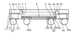
- 중앙에 일정크기의 관통공이 형성되어 있고, 상,하면에는 다수의 회로패턴이 형성된 제1섭스트레이트와;상기 제1섭스트레이트의 관통공 내측에 위치되어 있으며, 하면 내주연에 다수의 입출력패드가 형성된 제1반도체칩과;상기 제1반도체칩의 입출력패드와 상기 제1섭스트레이트의 회로패턴을 상호 연결하는 다수의 도전성와이어와;상기 제1반도체칩의 하면에 접착층으로 접착되어 있으며, 하면에는 다수의 입출력패드가 형성되어 있고, 상기 입출력패드에는 도전성범프가 융착된 제2반도체칩과;상기 제2반도체칩의 하면에 이방성도전필름에 의해 접착되어 있으며, 상,하면에 다수의 회로패턴이 형성된 제2섭스트레이트와;상기 제1섭스트레이트의 관통공 내측에 봉지되어 상기 제1반도체칩, 도전성와이어, 제2반도체칩 및 제2섭스트레이트의 외측을 봉지하는 봉지부와;상기 제1섭스트레이트 및 제2섭스트레이트의 회로패턴에 융착된 다수의 도전성볼을 포함하여 이루어진 반도체패키지.
- 제1항에 있어서, 상기 제1섭스트레이트의 상면에는 상기 제1반도체칩의 상면과 동일면을 이루며, 제1섭스트레이트의 관통공 폭보다 더 작은 폭의 관통공이 형 성된 경성(硬性)의 스티프너가 더 접착된 것을 특징으로 하는 반도체패키지.
- 제1항에 있어서, 상기 제1섭스트레이트 및 제2섭스트레이트의 회로패턴에 융착된 다수의 도전성볼은 모두 하면이 동일면인 것을 특징으로 하는 반도체패키지.
- 일정폭의 관통공이 형성된 스티프너 및 다수의 회로패턴이 상,하면에 형성되어 있으며, 상기 관통공과 중심이 같은 관통공을 갖는 제1섭스트레이트를 접착하고, 상기 스티프너의 상면에는 관통공이 폐색되도록 접착테이프를 접착하는 단계와;상기 스티프너의 관통공 내측인 접착테이프에, 하면에 다수의 입출력패드가 형성된 제1반도체칩을 접착하고, 상기 제1반도체칩의 입출력패드와 상기 제1섭스트레이트의 회로패턴을 도전성와이어로 상호 본딩하는 단계와;하면에 다수의 입출력패드가 형성되고, 상기 입출력패드에는 도전성범프가 융착된 제2반도체칩과, 상,하면에 다수의 회로패턴이 형성된 제2섭스트레이트를 준비하고, 상기 제2반도체칩의 도전성범프와 상기 제2섭스트레이트의 회로패턴을 상기 이방성도전필름을 개재하여 전기적으로 연결 및 접착하고, 상기 제2반도체칩, 이방성도전필름 및 제2섭스트레이트를 접착층을 개재하여 상기 제1반도체칩의 하면에 접착하는 단계와;상기 스티프너 및 제1섭스트레이트의 관통공 내측에 봉지재를 충진하여 일정형태의 봉지부를 형성하는 단계와;상기 제1섭스트레이트 및 제2섭스트레이트의 하면에 형성된 회로패턴에 다수의 도전성볼을 융착하는 단계를 포함하여 이루어진 반도체패키지의 제조 방법.
- 제4항에 있어서, 상기 봉지 단계 또는 도전성볼 융착 단계후에는 스티프너 상면의 접착테이프를 제거하는 단계가 더 포함된 것을 특징으로 하는 반도체패키지의 제조 방법.
Priority Applications (1)
| Application Number | Priority Date | Filing Date | Title |
|---|---|---|---|
| KR1020010049658A KR100708043B1 (ko) | 2001-08-17 | 2001-08-17 | 반도체패키지 및 그 제조 방법 |
Applications Claiming Priority (1)
| Application Number | Priority Date | Filing Date | Title |
|---|---|---|---|
| KR1020010049658A KR100708043B1 (ko) | 2001-08-17 | 2001-08-17 | 반도체패키지 및 그 제조 방법 |
Publications (2)
| Publication Number | Publication Date |
|---|---|
| KR20030015761A KR20030015761A (ko) | 2003-02-25 |
| KR100708043B1 true KR100708043B1 (ko) | 2007-04-16 |
Family
ID=27719602
Family Applications (1)
| Application Number | Title | Priority Date | Filing Date |
|---|---|---|---|
| KR1020010049658A Expired - Lifetime KR100708043B1 (ko) | 2001-08-17 | 2001-08-17 | 반도체패키지 및 그 제조 방법 |
Country Status (1)
| Country | Link |
|---|---|
| KR (1) | KR100708043B1 (ko) |
Citations (4)
| Publication number | Priority date | Publication date | Assignee | Title |
|---|---|---|---|---|
| JPH11219984A (ja) * | 1997-11-06 | 1999-08-10 | Sharp Corp | 半導体装置パッケージおよびその製造方法ならびにそのための回路基板 |
| JPH11260851A (ja) * | 1998-03-11 | 1999-09-24 | Matsushita Electric Ind Co Ltd | 半導体装置及び該半導体装置の製造方法 |
| US6077724A (en) * | 1998-09-05 | 2000-06-20 | First International Computer Inc. | Multi-chips semiconductor package and fabrication method |
| JP2001223326A (ja) * | 2000-02-09 | 2001-08-17 | Hitachi Ltd | 半導体装置 |
-
2001
- 2001-08-17 KR KR1020010049658A patent/KR100708043B1/ko not_active Expired - Lifetime
Patent Citations (4)
| Publication number | Priority date | Publication date | Assignee | Title |
|---|---|---|---|---|
| JPH11219984A (ja) * | 1997-11-06 | 1999-08-10 | Sharp Corp | 半導体装置パッケージおよびその製造方法ならびにそのための回路基板 |
| JPH11260851A (ja) * | 1998-03-11 | 1999-09-24 | Matsushita Electric Ind Co Ltd | 半導体装置及び該半導体装置の製造方法 |
| US6077724A (en) * | 1998-09-05 | 2000-06-20 | First International Computer Inc. | Multi-chips semiconductor package and fabrication method |
| JP2001223326A (ja) * | 2000-02-09 | 2001-08-17 | Hitachi Ltd | 半導体装置 |
Also Published As
| Publication number | Publication date |
|---|---|
| KR20030015761A (ko) | 2003-02-25 |
Similar Documents
| Publication | Publication Date | Title |
|---|---|---|
| US7679178B2 (en) | Semiconductor package on which a semiconductor device can be stacked and fabrication method thereof | |
| US7436061B2 (en) | Semiconductor device, electronic device, electronic apparatus, and method of manufacturing semiconductor device | |
| US7528007B2 (en) | Methods for assembling semiconductor devices and interposers | |
| US7256072B2 (en) | Semiconductor device, electronic device, electronic apparatus, and method of manufacturing semiconductor device | |
| US7230329B2 (en) | Semiconductor device, electronic device, electronic equipment, method of manufacturing semiconductor device, and method of manufacturing electronic device | |
| KR20010104217A (ko) | 반도체 장치 및 그 제조 방법, 회로 기판 및 전자 기기 | |
| US12616057B2 (en) | Double-sided sip packaging structure having interposer including a groove and manufacturing method thereof | |
| JP4069771B2 (ja) | 半導体装置、電子機器および半導体装置の製造方法 | |
| US6737590B2 (en) | Tape circuit board and semiconductor chip package including the same | |
| KR100401018B1 (ko) | 반도체패키지를 위한 웨이퍼의 상호 접착 방법 | |
| TWI395319B (zh) | 避免封裝堆疊接點斷裂之半導體組合構造 | |
| KR20030015761A (ko) | 반도체패키지 및 그 제조 방법 | |
| KR100533761B1 (ko) | 반도체패키지 | |
| KR100549299B1 (ko) | 반도체패키지 및 그 제조 방법 | |
| US20080237832A1 (en) | Multi-chip semiconductor package structure | |
| KR100401019B1 (ko) | 반도체패키지 및 그 제조방법 | |
| KR20010017869A (ko) | 멀티 칩 반도체 패키지 | |
| KR100337459B1 (ko) | 반도체패키지의 제조 방법 | |
| KR100406447B1 (ko) | 반도체패키지 및 그 제조방법 | |
| KR100379086B1 (ko) | 반도체패키지제조방법 | |
| KR20020077712A (ko) | 반도체패키지 및 그 제조 방법 | |
| KR100369387B1 (ko) | 반도체패키지 및 그 제조방법 | |
| KR100365052B1 (ko) | 반도체패키지 및 그 제조 방법 | |
| US20070222047A1 (en) | Semiconductor package structure | |
| KR20020088669A (ko) | 반도체칩의 스택킹 구조 및 그 방법 |
Legal Events
| Date | Code | Title | Description |
|---|---|---|---|
| PA0109 | Patent application |
St.27 status event code: A-0-1-A10-A12-nap-PA0109 |
|
| PG1501 | Laying open of application |
St.27 status event code: A-1-1-Q10-Q12-nap-PG1501 |
|
| A201 | Request for examination | ||
| PA0201 | Request for examination |
St.27 status event code: A-1-2-D10-D11-exm-PA0201 |
|
| D13-X000 | Search requested |
St.27 status event code: A-1-2-D10-D13-srh-X000 |
|
| D14-X000 | Search report completed |
St.27 status event code: A-1-2-D10-D14-srh-X000 |
|
| E701 | Decision to grant or registration of patent right | ||
| PE0701 | Decision of registration |
St.27 status event code: A-1-2-D10-D22-exm-PE0701 |
|
| PR1002 | Payment of registration fee |
St.27 status event code: A-2-2-U10-U11-oth-PR1002 Fee payment year number: 1 |
|
| GRNT | Written decision to grant | ||
| PR0701 | Registration of establishment |
St.27 status event code: A-2-4-F10-F11-exm-PR0701 |
|
| PG1601 | Publication of registration |
St.27 status event code: A-4-4-Q10-Q13-nap-PG1601 |
|
| PR1001 | Payment of annual fee |
St.27 status event code: A-4-4-U10-U11-oth-PR1001 Fee payment year number: 4 |
|
| PR1001 | Payment of annual fee |
St.27 status event code: A-4-4-U10-U11-oth-PR1001 Fee payment year number: 5 |
|
| PR1001 | Payment of annual fee |
St.27 status event code: A-4-4-U10-U11-oth-PR1001 Fee payment year number: 6 |
|
| FPAY | Annual fee payment |
Payment date: 20130408 Year of fee payment: 7 |
|
| PR1001 | Payment of annual fee |
St.27 status event code: A-4-4-U10-U11-oth-PR1001 Fee payment year number: 7 |
|
| FPAY | Annual fee payment |
Payment date: 20140408 Year of fee payment: 8 |
|
| PR1001 | Payment of annual fee |
St.27 status event code: A-4-4-U10-U11-oth-PR1001 Fee payment year number: 8 |
|
| PR1001 | Payment of annual fee |
St.27 status event code: A-4-4-U10-U11-oth-PR1001 Fee payment year number: 9 |
|
| FPAY | Annual fee payment |
Payment date: 20160406 Year of fee payment: 10 |
|
| PR1001 | Payment of annual fee |
St.27 status event code: A-4-4-U10-U11-oth-PR1001 Fee payment year number: 10 |
|
| FPAY | Annual fee payment |
Payment date: 20170407 Year of fee payment: 11 |
|
| PR1001 | Payment of annual fee |
St.27 status event code: A-4-4-U10-U11-oth-PR1001 Fee payment year number: 11 |
|
| PN2301 | Change of applicant |
St.27 status event code: A-5-5-R10-R13-asn-PN2301 St.27 status event code: A-5-5-R10-R11-asn-PN2301 |
|
| FPAY | Annual fee payment |
Payment date: 20180404 Year of fee payment: 12 |
|
| PR1001 | Payment of annual fee |
St.27 status event code: A-4-4-U10-U11-oth-PR1001 Fee payment year number: 12 |
|
| PR1001 | Payment of annual fee |
St.27 status event code: A-4-4-U10-U11-oth-PR1001 Fee payment year number: 13 |
|
| PR1001 | Payment of annual fee |
St.27 status event code: A-4-4-U10-U11-oth-PR1001 Fee payment year number: 14 |
|
| PR1001 | Payment of annual fee |
St.27 status event code: A-4-4-U10-U11-oth-PR1001 Fee payment year number: 15 |
|
| PC1801 | Expiration of term |
St.27 status event code: N-4-6-H10-H14-oth-PC1801 Not in force date: 20210818 Ip right cessation event data comment text: Termination Category : EXPIRATION_OF_DURATION |
|
| P22-X000 | Classification modified |
St.27 status event code: A-4-4-P10-P22-nap-X000 |