KR101282995B1 - Circulator/isolator - Google Patents
Circulator/isolatorInfo
- Publication number
- KR101282995B1 KR101282995B1 KR1020090046572A KR20090046572A KR101282995B1 KR 101282995 B1 KR101282995 B1 KR 101282995B1 KR 1020090046572 A KR1020090046572 A KR 1020090046572A KR 20090046572 A KR20090046572 A KR 20090046572A KR 101282995 B1 KR101282995 B1 KR 101282995B1
- Authority
- KR
- South Korea
- Prior art keywords
- cover
- housing body
- housing
- main body
- outer peripheral
- Prior art date
- Legal status (The legal status is an assumption and is not a legal conclusion. Google has not performed a legal analysis and makes no representation as to the accuracy of the status listed.)
- Expired - Fee Related
Links
Images


Classifications
-
- H—ELECTRICITY
- H01—ELECTRIC ELEMENTS
- H01P—WAVEGUIDES; RESONATORS, LINES, OR OTHER DEVICES OF THE WAVEGUIDE TYPE
- H01P1/00—Auxiliary devices
- H01P1/32—Non-reciprocal transmission devices
- H01P1/38—Circulators
- H01P1/383—Junction circulators, e.g. Y-circulators
- H01P1/387—Strip line circulators
-
- H—ELECTRICITY
- H01—ELECTRIC ELEMENTS
- H01P—WAVEGUIDES; RESONATORS, LINES, OR OTHER DEVICES OF THE WAVEGUIDE TYPE
- H01P1/00—Auxiliary devices
- H01P1/32—Non-reciprocal transmission devices
- H01P1/36—Isolators
-
- H—ELECTRICITY
- H01—ELECTRIC ELEMENTS
- H01P—WAVEGUIDES; RESONATORS, LINES, OR OTHER DEVICES OF THE WAVEGUIDE TYPE
- H01P11/00—Apparatus or processes specially adapted for manufacturing waveguides or resonators, lines, or other devices of the waveguide type
Landscapes
- Non-Reversible Transmitting Devices (AREA)
Abstract
본 발명의 일측면에 따른 비가역 회로소자는, 측벽과 바닥부를 구비하여 내측에 수납 공간을 형성하는 하우징 본체; 상기 하우징 본체의 수납 공간에 순차 적층되어 수납된 하부 페라이트, 정션(junction), 상부 페라이트, 극판(pole piece) 및 마그네트(magnet)를 포함하는 적층 부품; 및 상기 하우징 본체의 상부에서 하우징 본체와 결합되는 커버를 포함한다. 상기 커버는 탑부(top portion)와 측면 외주부를 구비하되, 상기 측면 외주부에는, 상기 측면 외주부의 일 지점으로부터 내측 상방으로 돌출된 복수의 후크(hook)부가 구비되어 있다. 상기 하우징 본체의 측벽 상단에는 상기 커버와 하우징 본체간의 체결을 위해 상기 후크부가 하면에 걸리도록 상기 측벽 외측으로 돌출된 걸림 돌기부가 구비되어 있다. An irreversible circuit device according to an aspect of the present invention includes a housing body having sidewalls and a bottom portion to form an accommodation space therein; A laminated component including a lower ferrite, a junction, an upper ferrite, a pole piece, and a magnet, which are sequentially stacked and received in an accommodation space of the housing body; And a cover coupled to the housing body at an upper portion of the housing body. The cover includes a top portion and a side outer periphery, and the side outer periphery includes a plurality of hook portions protruding inwardly upward from one point of the side outer periphery. The upper end of the side wall of the housing body is provided with a locking protrusion protruding outside the side wall so that the hook portion is caught on the lower surface for fastening between the cover and the housing body.
비가역 회로소자, 서큘레이터, 아이솔레이터 Irreversible Circuitry, Circulators, Isolators
Description
본 발명은 중계기 등의 무선통신 시스템에 사용되는 비가역 회로소자(circulator/isolator)에 관한 것으로, 특히 드롭인(drop-in)형 서큘레이터/아이솔레이터로 적합하고 하우징 구조와 커버간의 결합이 안정적이고 신뢰성이 높으며 커버의 체결과 분리가 용이하여 튜닝이나 수리에 유리한 비가역 회로소자에 관한 것이다.The present invention relates to an irreversible circuit device (circulator / isolator) used in a wireless communication system such as a repeater, in particular suitable as a drop-in type circulator / isolator, and the coupling between the housing structure and the cover is stable and reliable The present invention relates to an irreversible circuit element having a high and easy to fasten and detach a cover, which is advantageous for tuning or repair.
비가역 회로소자, 즉 서큘레이터/아이솔레이터(circulator/isolator)는 페라이트의 마이크로파 회전 현상을 이용한 비가역적 특성을 갖는 수동부품으로, 주로 무선통신 시스템에 채용되어 파워 앰프의 안정적 동작, 임피던스 정합, 반사파 제거 등의 기능을 수행하여 무선통신 시스템의 안정화에 중요한 역할을 한다. 서큘레이터는 입력된 역방향 신호나 반사파가 입력측으로 가지 않게 하는 비가역성과 순환성을 가지며, 서큘레이터의 일 단자에 연결된 종단 저항을 설치하여 아이솔레이터를 구현할 수 있다. An irreversible circuit element, ie, a circulator / isolator, is a passive component that has an irreversible characteristic using a microwave rotation phenomenon of ferrite, and is mainly adopted in a wireless communication system to provide stable operation of power amplifiers, impedance matching, and elimination of reflected waves. It plays an important role in stabilizing wireless communication system by performing the function of. The circulator has irreversibility and circulation that prevents the inputted reverse signal or the reflected wave from going to the input side, and it can implement the isolator by providing the terminal resistance connected to one terminal of the circulator.
이러한 비가역 회로소자는, 이동통신 단말기나 중계기 등에 적용되며 소형화에 적합한 집중정수(lumped element)형 소자와, 기지국 등의 고출력 시스템에 적용되는 분포정수(distributed element)형 소자로 구분될 수 있다. 드롭인 서큘레이터/아이솔레이터는 분포정수형 비가역 회로소자로서, 스트립 라인 Y 접합(strip line Y junction)의 형태로 구현된다. 드롭인 아이솔레이터는 다른 분포정수형 소자에 비해 소형화 및 경량화에 유리하고 삽입 손실과 아이솔레이션 등의 특성이 좋으며 쉽게 광대역화할 수 있다. Such an irreversible circuit device may be classified into a lumped element type device, which is applied to a mobile communication terminal, a repeater, and the like, and a distributed element type device that is applied to a high output system such as a base station. The drop-in circulator / isolator is a distributed integer irreversible circuit element, which is implemented in the form of a strip line Y junction. The drop-in isolator is advantageous for miniaturization and weight reduction compared to other distributed constant devices, has good characteristics such as insertion loss and isolation, and can be easily broadband.
드롭인 아이솔레이터는 시스템의 고출력화에 적합하도록 허용 전력 범위가 높아지는 경향이 있다. 출력 파워가 높아질수록, 아이솔레이터 내의 페라이트의 비선형 특성으로 발생하는 IMD(Intermodulation) 특성 중 3차 IMD 효과가 두드러진다. 따라서, 이러한 3차 IMD 효과를 최소화할 수 있는 방안이 필요하다. 특히, 협대역 특성을 갖는 로우 IMD(low IMD) 제품이나 특성 요구 수준이 매우 높은 제품의 경우, 조립 부품들의 튜닝을 통해 3차 IMD 효과를 억제할 필요가 있다. Drop-in isolators tend to have a higher allowable power range for higher system outputs. As the output power increases, the third-order IMD effect becomes more prominent among the intermodulation (IMD) characteristics caused by the nonlinear characteristics of the ferrite in the isolator. Therefore, there is a need for a method capable of minimizing such tertiary IMD effects. In particular, in the case of a low IMD product having a narrow band characteristic or a product having a very high level of characteristic demand, it is necessary to suppress the tertiary IMD effect by tuning the assembly parts.
기존의 일반적인 드롭인 서큘레이터/아이솔레이터의 하우징은 기계가공(machining)에 의해 일체로 제작되어, 가공 비용이 높고 제작기간이 오래 걸리는 단점이 있다. 대량 생산에 적합하고 저가의 하우징 제작을 위해 기계가공이 아닌 프레스(press) 금형으로 가공된 하우징이 제작되고 있다(도 1a, 1b).Existing general drop-in circulator / isolator housing is manufactured integrally by machining (machining), there is a disadvantage that the processing cost is high and the production period takes a long time. Housings that have been processed with press molds, rather than machined, are being manufactured for production of low cost housings suitable for mass production (FIGS. 1A and 1B).
도 1a는 종래의 비가역 회로소자의 하우징 구조와 커버를 나타낸 조립 사시도이고, 도 1b는 도 1a의 하우징 구조를 사용한 비가역 회로소자(10)의 조립 사시도이다. 도 1a를 참조하면, 하우징 구조는, 프레스 가공에 의한 바닥 플레이트(bottom plate: 11)와 원통형 하우징 본체(housing body: 12)를 포함한다. 하우징 본체(12)의 측벽에 단자 수용홈(12a)들이 형성되어 있다.FIG. 1A is an assembled perspective view illustrating a housing structure and a cover of a conventional non-reciprocal circuit element, and FIG. 1B is an assembled perspective view of the
하우징 본체(12)의 하면에 구비된 체결용 돌기부(15a)가 바닥 플레이트(11)의 구멍(11a)에 단순 압입됨으로써 하우징 본체(12)와 바닥 플레이트(11)가 서로 결합된다. 하우징 구조의 결합 후에는, 도 1b에 도시된 바와 같이, 하우징 본체(12)의 수용 공간 내에 하부 페라이트(lower ferrite: 16a), 정션(junction: 17), 상부 페라이트(upper ferrite: 16b), 극판(pole piece: 18), 마그네트(magnet: 19), 온도 보상판(temperature compensator: 22) 등의 아이솔레이터 부품을 적층하여 넣는다. 최종적으로 하우징 본체(12)의 상부를 덮도록 캔(can) 형태의 커버(13)를 하우징 본체(12)에 눌러, 커버(13)를 하우징 본체(12)에 체결한다. 비가역 회로소자(10)는 기판 체결용 홀(11b)을 통해 회로 기판에 실장될 수 있다. The housing
그러나, 캔 타입의 커버(13)를 사용하여 하우징을 캡핑할 경우, 커버(13)를 일단 체결하면 커버(13)를 더이상 분리할 수 없고(캔 타입의 커버(13)를 강제로 분리할 경우 하우징 내부의 내용물이나 하우징 구조 자체가 손상되기 쉬움) 커버의 재사용이 불가하므로, 아이솔레이터 부품의 튜닝이나 수리가 거의 불가능하게 되 고, 튜닝을 통한 3차 IMD 효과의 억제가 어려워지게 된다. However, when capping the housing using the can type
또한, 하우징 본체(12)와 바닥 플레이트(11)를 단순압입에 의해 체결하는 경우에는, 하우징 본체(12)와 바닥 플레이트(11) 간의 결합력이 충분하지 못하여 외부의 충격 등으로 인해 하우징 본체(12)가 바닥 플레이트(11)로부터 분리 또는 이탈될 수 있다. 이에 따라 비가역 회로소자(10)의 접지(ground)성이 떨어져 아이솔레이션 특성의 변경이 초래되고 제품의 장기적인 신뢰성에 악영향을 미치게 된다.In addition, when the housing
본 발명의 일측면은 상술한 문제를 해결하기 위한 것으로서, 하우징 본체와 커버의 결합이 용이하고 커버의 분리와 반복적 체결을 통해서 필요한 튜닝이나 수리가 용이한 저가형 비가역 회로소자를 제공하는 것이다. 또한, 본 발명의 일측면은 하우징 구조의 결합력이 강하고 안정적이며 대량생산에 적합한 저가형 비가역 회로소자를 제공하는 것이다. One aspect of the present invention is to solve the above-mentioned problems, to provide a low-cost irreversible circuit element that is easy to combine the housing body and the cover, and easy tuning or repair necessary by separating and repeatedly tightening the cover. In addition, one aspect of the present invention is to provide a low-cost irreversible circuit device having a strong bonding force of the housing structure, stable and suitable for mass production.
본 발명의 일측면에 따른 비가역 회로소자는, 측벽과 바닥부를 구비하여 내측에 수납 공간을 형성하는 하우징 본체; 상기 하우징 본체의 수납 공간에 적층되어 수납된 하부 페라이트, 정션(junction), 상부 페라이트, 극판(pole piece) 및 마그네트(magnet)를 포함하는 적층 부품; 및 상기 하우징 본체의 상부에서 하우징 본체와 결합되는 커버를 포함한다. 상기 커버는 탑부(top portion)와 측면 외주부를 구비하되, 상기 측면 외주부에는, 상기 측면 외주부의 일 지점으로부터 내측 상방으로 돌출된 복수의 후크(hook)부가 구비되어 있다. 상기 하우징 본체의 측벽 상단에는 상기 커버와 하우징 본체간의 체결을 위해 상기 후크부가 하면에 걸리도록 상기 측벽 외측으로 돌출된 걸림 돌기부가 구비되어 있다. An irreversible circuit device according to an aspect of the present invention includes a housing body having sidewalls and a bottom portion to form an accommodation space therein; A laminated component including a lower ferrite, a junction, an upper ferrite, a pole piece, and a magnet, which are stacked and received in an accommodation space of the housing body; And a cover coupled to the housing body at an upper portion of the housing body. The cover includes a top portion and a side outer periphery, and the side outer periphery includes a plurality of hook portions protruding inwardly upward from one point of the side outer periphery. The upper end of the side wall of the housing body is provided with a locking protrusion protruding outside the side wall so that the hook portion is caught on the lower surface for fastening between the cover and the housing body.
본 발명의 실시형태에 따르면, 상기 복수의 후크부는 상기 커버의 측면 외주 부를 따라 인접하여 배치된 1쌍의 후크부를 포함하되, 상기 커버와 하우징 본체의 결합 상태에서 상기 1쌍의 후크부 사이에 위치하여 상기 후크부의 좌우 이동을 막도록 상기 걸림 돌기부의 일 지점으로부터 아래로 연장된 좌우회전 스토퍼(stropper)부가 구비될 수 있다. 상기 좌우회전 스토퍼는 상기 1쌍의 후크부와 결합하는 걸림 돌기부의 중간 지점 설치될 수 있다.According to an embodiment of the present invention, the plurality of hook portions includes a pair of hook portions disposed adjacently along the side outer periphery of the cover, and positioned between the pair of hook portions in an engaged state of the cover and the housing body. In order to prevent the left and right movement of the hook portion may be provided with a left and right rotation stopper (stropper) extending downward from one point of the locking projection. The left and right rotation stoppers may be installed at an intermediate point of the engaging protrusion coupled to the pair of hook portions.
본 발명의 실시형태에 따르면, 상기 후크부와 걸림 돌기부 간의 조립을 안내하도록 상기 걸림 돌기부로부터 연장되어 상기 하우징 본체의 측벽 외측으로 더 돌출된 후크 조립용 가이드부가 상기 걸림 돌기부 단부측에 구비될 수 있다. 상기 후크 조립용 가이드부는 1쌍의 후크부와 결합하는 걸림 돌기부의 양단에 배치될 수 있다.According to an embodiment of the present invention, the hook assembly guide portion extending from the locking protrusion to further protrude outward of the side wall of the housing body to guide the assembly between the hook portion and the locking protrusion may be provided at the end of the locking protrusion. . The hook assembly guide portion may be disposed at both ends of the engaging protrusion coupled with the pair of hook portions.
본 발명의 실시형태에 따르면, 상기 하우징 본체에 체결된 커버는, 상기 하우징 본체에 대한 상기 커버의 회전운동에 의해서 상기 하우징 본체로부터 분리가능하다. 상기 커버의 측면 외주부에는 상기 커버의 분리를 위한 분리 지그의 분리용 바(bar)가 끼워질 수 있도록 커버 내측으로 함몰된 분리홈이 형성될 수 있다.According to the embodiment of the present invention, the cover fastened to the housing main body is detachable from the housing main body by the rotational movement of the cover with respect to the housing main body. Separation grooves recessed inside the cover may be formed in the outer peripheral portion of the side of the cover to be fitted with a separation bar of the separation jig for separating the cover.
본 발명의 실시형태에 따르면, 상기 커버의 탑부는 상기 적층 부품을 아래로 눌러주는 힘을 제공하도록 아래로 함몰된 구조를 가질 수 있다. According to an embodiment of the present invention, the top portion of the cover may have a structure recessed downward to provide a force for pressing the laminated component down.
본 발명의 실시형태에 따르면, 상기 비가역 회로소자는, 상기 하우징 본체의 바닥부 하면에 결합된 바닥 플레이트를 더 포함할 수 있다. 상기 바닥 플레이트 상면에는 위로 돌출된 복수의 엠보싱부가 형성되어 있고, 상기 엠보싱부는 상기 하우징 본체의 바닥부에 형성된 엠보싱부 체결용 구멍에 삽입되어 상기 바닥 플레이트가 상기 하우징에 결합하되, 상기 엠보싱부의 상하로 가해진 압축력에 의해 상기 엠보싱부가 외측으로 확장되어 상기 엠보싱부 체결용 구멍의 내벽에 접촉 고정될 수 있다. According to an embodiment of the present invention, the irreversible circuit element may further include a bottom plate coupled to the bottom surface of the bottom of the housing body. The upper surface of the bottom plate is formed with a plurality of embossed protruding upwards, the embossed portion is inserted into the hole for fastening the embossed portion formed in the bottom portion of the housing main body and the bottom plate is coupled to the housing, the upper and lower embossed portion The embossed portion may be extended outward by the applied compressive force to be fixed to the inner wall of the hole for fastening the embossed portion.
본 발명의 실시형태에 따르면, 상기 하우징 본체의 바닥부는 솔더링 홀(soldering hole)을 갖되, 상기 솔더링 홀에 충진된 솔더링 접합제를 통해 상기 바닥 플레이트와 하우징 본체가 서로 접합될 수 있다. According to an embodiment of the present invention, the bottom portion of the housing body has a soldering hole (soldering hole), the bottom plate and the housing body may be bonded to each other through a soldering filler filled in the soldering hole.
본 발명의 실시형태에 따르면, 상기 하우징 본체의 바닥부와 벽면이 직각(90°)을 유지하도록 상기 바닥부와 벽면의 경계부에 위치하는 상기 하우징 본체의 내경 안쪽에 Z-벤딩(Z-bending)이 형성될 수 있다.According to an embodiment of the present invention, a Z-bending inside the inner diameter of the housing body located at the boundary between the bottom portion and the wall surface such that the bottom portion and the wall surface of the housing body maintain a right angle (90 °). This can be formed.
본 발명의 실시형태에 따르면, 상기 비가역 회로소자는, 상기 커버 상부에서 상기 커버와 결합되고 진공 흡착이 가능하도록 평평한(평탄한) 상면을 갖는 커버 리드(cover lid)를 더 포함할 수 있다. According to an embodiment of the present invention, the irreversible circuit element may further include a cover lid having a flat (flat) top surface coupled to the cover on the cover and capable of vacuum adsorption.
본 발명의 실시형태에 따르면, 상기 하우징 본체는, 상기 하우징 본체의 측면 외주부로부터 외측으로 연장되어 삽입 구멍이 뚫려있는 복수의 지지편을 구비하되, 상기 지지편의 구멍에는 SMT 핀 조립체가 삽입되어 결합될 수 있다. 상기 SMT 핀 조립체는 중심부에 구멍이 형성된 사출물과 상기 사출물의 구멍에 끼워진 중심 핀을 포함할 수 있다. 상기 중심핀의 상부는 상기 정션의 단자와 접속하고 상기 중심핀의 하부는 회로기판(PCB 등)에 표면실장될 수 있다. According to an embodiment of the present invention, the housing main body includes a plurality of support pieces extending outward from the outer peripheral portion of the side of the housing main body and having an insertion hole therein, wherein the SMT pin assembly is inserted into and coupled to the holes of the support pieces. Can be. The SMT pin assembly may include an injection molded product having a hole in a central portion thereof and a center pin inserted into the hole of the injection molded product. An upper portion of the center pin may be connected to a terminal of the junction, and a lower portion of the center pin may be surface mounted on a circuit board (PCB, etc.).
본 발명에 따르면, 하우징 본체와 커버 간의 체결과 분리가 용이하고 커버 구조의 신뢰성이 높으며, 조립 부품들의 튜닝을 쉽게 할 수 있다. 이로써, 3차 IMD 효과등을 억제시키기에 유리하고, 협대역의 특성을 갖고 있는 로우 IMD 제품이나 특성 요구가 높은 제품의 생산에 적합하다. 뿐만 아니라, 엠보싱부의 가체결과 가압 코킹을 통해 바닥 플레이트, 하우징 본체를 결합함으로써, 하우징 구조의 결합력과 내구성을 크게 개선할 수 있으며, 전기적 접지 능력을 높일 수 있다.According to the present invention, the fastening and detachment between the housing main body and the cover is easy, the reliability of the cover structure is high, and the assembly parts can be easily tuned. This is advantageous for suppressing the tertiary IMD effect and the like, and is suitable for the production of low IMD products having narrow band characteristics and high demand products. In addition, by combining the bottom plate and the housing body through the embossing portion and the pressure caulking, the bonding force and durability of the housing structure can be greatly improved, and the electrical grounding ability can be enhanced.
이하, 첨부된 도면을 참조하여 본 발명의 실시형태를 설명한다. 그러나, 본 발명의 실시형태는 여러가지 다른 형태로 변형될 수 있으며, 본 발명의 범위가 이하 설명하는 실시형태로 한정되는 것은 아니다. Hereinafter, embodiments of the present invention will be described with reference to the accompanying drawings. However, embodiments of the present invention may be modified in various other forms, and the scope of the present invention is not limited to the embodiments described below.
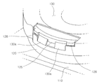
도 2는 본 발명의 실시형태에 따른 비가역 회로소자의 조립 사시도이다. 도 2를 참조하면, 하우징 본체(120)는 위로 개방된 원통 형상으로서 3개의 단자 수용홈(122)이 형성된 측벽과 바닥부를 구비하며, 아래의 바닥 플레이트(110)와 결합되어 있다. 이 하우징 본체(120)은 서큘레이터/아이솔레이터 조립 부품들(적층부품들)이 적층하여 내장되는 수납 공간을 형성한다. 후술하는 바와 같이, 커버(130)의 측면 외주부에 구비된 후크부(130a)가 하우징 본체(120)의 걸림 돌기부(124)에 걸림으로써 하우징 본체(120)는 커버(130)와 용이하게 체결된다. 2 is an assembled perspective view of an irreversible circuit element according to an embodiment of the present invention. Referring to FIG. 2, the housing
하우징 본체(120)의 수납 공간에는, 하부 페라이트(165a), 정션(170), 상부 페라이트(165b), 극판(180), 접지 플레이트(185), 마그네트(190), 온도 보상판(220)이 순차적으로 적층되어 있다. 상하부 페라이트(165a, 165b)로는 예컨대 가넷(garnet)계 연자성체를 사용할 수 있다. 정션(170)은 중심체 도체에 해당하며 3 방향으로 연장된 3개의 단자(170a, 170b, 170b)를 구비한다. The
부가적으로, 공진기 기능에 중요한 정션(170) 및 페라이트(165a, 165b)를 정렬시키도록 하부 페라이트(165a) 아래에 중심 정렬 플레이트(160)을 배치시킬 수 있다. 정션(170)과 페라이트(165a, 165b)들 간의 정렬불량은 RF 특성에 영향을 주고 정확한 특성 구현을 어렵게 만든다. 중심 정렬 플레이트(160)의 외주로부터 위로 돌출된 복수의 가이드 편(160a) 내측에, 정션(170) 및 페라이트(165a, 165b) 등을 안치함으로써 이들 부품을 수직으로 정렬시킬 수 있다. 중심 정렬 플레이 트(160) 대신에 복수의 가이드 편을 갖는 링 형상의 얼라이너를 사용할 수도 있다.Additionally,
또한 하우징 본체(120)의 수납 공간 내에서, 마크네트(190)의 측면을 둘러싸는 측벽 스페이서(210)를 더 배치할 수 있다. 수납 공간 내에서 마그네트(190)의 위치이동으로 인한 자계와 소자 특성의 변화를 방지하기 위해 마그네트(190)의 측면 공간 - 하우징 본체(120) 안으로 부품조립을 할 수 있도록 통상적으로 하우징 본체(120)의 내경은 마그네트(190)와 같은 적층 부품의 지름보다 큼 - 을 측벽 스페이서(210)로 둘러싸서 마그네트(190)를 수납 공간 내에 안정적으로 고정시킬 수 있다. 측벽 스페이서(210)는 내열성 폴리머로 형성되고, 특히 일 지점이 끊어진 절개부(210a)를 가져 설치가 용이하고 설치시 파손이 방지된다.In addition, the
또한 하우징 본체(120)의 수납 공간 내에는, 커버(130)와 마그네트(190) 사이에 탑 플레이트(230)를 더 배치할 수도 있다. 탑 플레이트(230)는 그 외주로부터 외측으로 돌출 연장된 복수의 돌출편(230)을 구비한다. 복수의 돌출편(230)이 단자 수용홈(122)에 걸쳐 있기 때문에, 커버(130) 체결을 위해 커버(130)를 돌리더라도 탑 플레이트(230)는 돌지 않게 된다. 이러한 탑 플레이트(230)를 사용함으로써 개폐를 위한 커버(130) 회전시 커버 아래의 가넷, 극판 등의 부품이 함께 돌아가거나 정렬이 틀어지는 것을 막을 수 있다. In addition, the
도 3은 본 발명의 실시형태에 따른 비가역 회로소자의 하우징 본체와 커버를 나타낸 조립 사시도이며, 도 4는 도 3의 비가역 회로소자의 조립 완성된 상태를 나타낸 사시도이다. 도 3을 참조하면, 하우징 본체(120)는 측벽과 바닥부를 구비하여 내측에 수납 공간이 형성되어 있으며, 이 수납 공간에 하부 페라이트, 정션, 상부 페라이트, 극판 및 마그네트 등의 적층 부품(50)이 적층되어 있다. 또한, 커버(130)가 하우징 본체(120)의 상부에서 하우징 본체(120)와 결합되어 있다. 커버(130)는 탑부와 측면 외주부를 구비한다. 3 is an assembled perspective view illustrating a housing main body and a cover of the irreversible circuit element according to the embodiment of the present invention, and FIG. 4 is a perspective view illustrating a completed state of the irreversible circuit element of FIG. 3. Referring to FIG. 3, the housing
커버(130)의 측면 외주부에는 일 지점으로부터 내측 상방으로 돌출된 복수의 후크부(130a)가 구비되어 있다. 이 후크부(130a)는, 도 3에 도시된 바와 같이 커버(130)의 측면 외주부의 일부를 절개하여 내측으로 밀어넣음으로써 형성될 수 있다. 또한, 하우징 본체(120)의 측벽 상단에는 커버(130)와 하우징 본체(120)간의 체결을 위해 하우징 본체(120)의 측벽 외측으로 돌출된 걸림 돌기부(124)가 구비되어 있다. 커버(130)와 하우징 본체(120)의 결합시, 후크부(130a)는 걸림 돌기부(124)의 하면에 걸려, 커버(130)와 하우징 본체(120)간의 체결이 안정적으로 이루어진다. 이러한 후크부(130a)와 걸림 돌기부(124) 간의 체결 구조는, 커버를 하우징 본체쪽으로 아래로 눌러줌으로써 다른 도구 없이 원 터치 방식으로 손쉽고 안정적으로 조립되며 별도의 탭가공이 필요없다. 또한 커버의 회전에 의해 커버나 내장 부품의 손상없이 커버 분리가 가능하여 부품 튜닝이나 수리를 위해 커버(130)를 개방하거나 재결합하기가 용이하다. 커버(130)의 탑부(130c)는 내장된 적층부품(50)을 하방으로 눌러주도록 아래로 함몰된 구조를 가질 수 있다. The outer peripheral portion of the side surface of the
바닥 플레이트(110)는 후술하는 바와 같이 엠보싱부의 가체결과 상하로 가압되는 코킹에 의해 하우징 본체(120)의 하면에 안정적이고 견고하게 결합될 수 있다(도 9, 10 참조). 정션의 단자(170c)는 단자 수용홈을 통해 외부로 노출되고 이 단자(170c)에 연결된 종단 저항기(270)를 설치하여 아이솔레이터를 구현할 수 있다. 상술한 바와 같이 바닥 플레이트(110), 하우징 본체(120), 적층 부품(50) 및 커버(130)의 조립이 완성되면, 도 4에 도시된 바와 같은 비가역 회로소자를 얻을 수 있다. 이러한 비가역 회로소자는, 바닥 플레이트(110)에 형성된 기판 체결용 홀(110b)을 통해 회로 기판(도시 안함)에 실장될 수 있다. The
도 5 및 6을 참조하여, 전술한 하우징 본체(120)와 커버(130)의 체결 구조를 더 상세히 설명한다. 도 5 및 6에 도시된 바와 같이, 커버(130)의 측면 외주부를 따라 인접하여 배치된 1쌍의 후크부(130a)가 구비될 수 있는데, 이러한 후크부(130a)의 쌍이 커버 외주부 전체에 걸쳐 3개(3쌍) 배치될 수 있다. 이에 따라 각 후크부(130a) 쌍에 대응하는 걸림 돌기부(124)를 하우징 본체(120)의 측벽 전체에 걸쳐 3군데 형성할 수 있다(도 3 참조). 5 and 6, the fastening structure of the
커버(130)와 하우징 본체(120)의 결합 상태에서 서로 인접한 1쌍의 후크부(130a)는 하우징 본체(120)의 걸림 돌기부(124)에 걸려서 커버(130)를 상측으로 구속시킨다. 또한, 도 6에 도시된 바와 같이, 커버(130)와 하우징 본체(120)의 결 합 상태에서 서로 인접한 1쌍의 후크부(130a) 사이에는 걸림 돌기부(124)의 일 지점(으로부터 아래로 연장된 좌우회전 스토퍼부(125)가 구비되어, 후크부(130a)의 좌우방향으로 구속시킨다. 후크부(130a)는 이 좌우회전 스토퍼부(125)에 의해 측방향(좌우방향)으로의 이동이 방지된다. 이러한 후크부(130a)쌍-걸림 돌기부(124)-좌우회전 스토퍼(125)의 체결 구조가 하우징 본체(120)의 전체 외주를 거쳐 3군데 배치됨으로써 커버와 하우징 본체 간의 안정적이고 용이한 체결이 이루어지게 된다. 좌우회전 스토퍼(125)는 1쌍의 후크부(130a)와 결합하는 걸림 돌기부(124)의 중간 지점 설치될 수 있다.The pair of
또한, 커버(130)와 하우징 본체(120)간의 체결을 보다 용이하고 빠르게 수행할 수 있도록, 후크부(130a)와 걸림 돌기부(124) 간의 조립을 안내하는 조립용 가이드부(126)가 구비될 수 있다. 이 조립용 가이드부(126)는 걸림 돌기부(124) 단부측에서 연장되어 하우징 본체(120)의 측벽 외측으로 (걸림 돌기부(124)보다) 더 돌출되어 있다. 이렇게 돌출된 가이드부(126)를 통해, 커버와 하우징 본체간 체결시 커버(130)의 후크(130a)를 대응하는 걸림 돌기부(124) 위치에 쉽게 위치시킬 수 있다. 후크 조립용 가이드부(126)는 1쌍의 후크부(130a)와 결합하는 걸림 돌기부(124)의 양단에 배치될 수 있다.In addition, the
도 7은 본 발명의 실시형태에 따른 커버 구조를 나타내는 단면도이며, 도 8은 도 7의 커버가 체결된 비가역 회로소자의 개략적인 단면도이다. 도 7 및 8을 참 조하면, 상술한 바와 같이 커버(130)의 측면 외주부에는 일부가 절개되어 내측으로 눌려져 돌출된 후크부(130a)가 구비되어 있고, 또한 커버(130)의 탑부(130c)는 아래로 함몰된 구조를 갖고 있다. 아래로 함몰된 탑부(130c)는 하우징 본체(120) 내에 수납된 적층 부품들을 아래로 눌러줌으로써(이에 따라 적층부품은 커버에 대해 밀어올리는 힘을 가하게 됨) 텐션(tension) 구조를 구현하게 되고, 이에 따라 내장된 적층 부품을 안정적으로 잡아주게 된다. 7 is a cross-sectional view showing a cover structure according to an embodiment of the present invention, and FIG. 8 is a schematic cross-sectional view of the irreversible circuit element to which the cover of FIG. 7 is fastened. Referring to FIGS. 7 and 8, as described above, the side outer peripheral portion of the
도 9는 본 발명의 실시형태에 따른 비가역 회로소자의 하우징 본체(120)와 바닥 플레이트(130) 간의 체결 구조를 설명하기 위한 조립 사시도(a) 및 바닥 플레이트의 부분 단면도(b)이다. 도 9를 참조하면, 바닥 플레이트(110)의 상면에는 위로 돌출된 복수의 엠보싱부(110a)가 형성되어 있다. 이 엠보싱부(110a)는, 예를 들어 적절한 정으로 바닥 플레이트(110)를 치거나 프레스 가공을 통해 형성할 수 있다. 9 is an assembled perspective view (a) and a partial cross-sectional view (b) of the bottom plate for explaining a fastening structure between the
엠보싱부(110a)는 하우징 본체(120)의 바닥부에 형성된 엠보싱부 체결용 구멍(120a)에 삽입되어 바닥 플레이트(110)가 하우징 본체(120)에 결합된다. 특히, 엠보싱부(110a)가 구멍(120a)에 삽입된 상태에서 엠보싱부(110a)의 상하로 가해진 압축력에 의해 엠보싱부(110a)가 외측으로 확장됨으로써, 엠보싱부(110a)가 엠보싱부 체결용 구멍(120a)의 내벽에 견고하게 접촉 고정된다. 이로써, 도 10에 도시된 바와 같은 하우징 체결 구조(하우징 본체(120) 및 바닥 플레이트(110)간의 체결 구 조)를 얻게 된다. The
도 11 및 12의 단면도를 참조하여, 하우징 본체(120)와 바닥 플레이트(110) 간의 체결 구조를 더 상세히 설명한다. 먼저, 도 11에 도시된 바와 같이, 바닥 플레이트(110)의 엠보싱부(110a)를 하우징 본체 바닥부(120d)에 형성된 구멍에 단순히 삽입하는 가체결을 한다. 이와 같이 가체결된 상태에서, 도 12에 도시된 바와 같이, 적절한 프레스 도구 또는 정(30, 40)을 사용하여, 엠보싱부(110a)를 중심으로 엠보싱부(110a)의 상하로부터 압축력(화살표 참조)을 가해서 엠보싱부(110a)가 외측으로 확장시키거나 퍼지게 한다. 이로써, 엠보싱부(110a)의 최외곽 지금이 커지게 되며, 엠보싱부(110a)와 바닥부(120d)의 구멍 내벽 간에 마찰력이 증대된다. 결국, 엠보싱부(110a)가 구멍 내벽에 강하게 접촉 고정되면서 하우징 본체(120)와 바닥 플레이트(110) 간에 결합력이 증대된다. 11 and 12, a fastening structure between the
도 13은 하우징 본체와 바닥 플레이트 간의 체결력을 강화하기 위한 솔더링을 설명하기 위한 도면이다. 도 13에 도시된 바와 같이, 하우징 본체(120)의 바닥부에는 솔더링 홀(soldering hole, 120b)이 형성되어 있다. 솔더 공급 수단(60)을 사용하여, 이 솔더링 홀(120b)에 솔더링 접합제(예컨대, 솔더링 페이스트)를 충진하고 열처리할 수 있다. 이로써, 바닥 플레이트(110)와 하우징 본체(120)간의 결합력을 더욱 더 강화시킴과 아울러, 하우징 본체(120)와 바닥 플레이트(110)의 접지(ground) 능력을 높일 수 있다.FIG. 13 is a diagram for describing soldering for enhancing fastening force between the housing body and the bottom plate. As shown in FIG. 13, a
도 14는 분리 지그에 의한 커버의 분리를 설명하기 위한 도면이다. 도 3 내지 4을 참조하여 설명한 바와 같이 커버(130)와 하우징 본체(120)는 후크부와 걸림 돌기부의 체결 구조를 통해 용이하고 안정적으로 체결될 수 있을 뿐만 아니라 분리 지그를 사용하여 (하우징 본체에 대한 커버의 회전 운동에 의해) 커버를 하우징 본체로부터 안정적으로 개방할 수 있다. 도 14에 도시된 바와 같이, 커버(130)의 측면 외주부에는 분리 지그(70)의 분리용 바(70a)가 끼워질 수 있도록 커버 내측으로 함몰된 분리홈(130b)가 형성되어 있다. 커버의 분리를 위한 분리 지그(70)의 분리용 바(70a)가 분리홈(130b)에 끼워진 상태에서 분리 지그(70)를 회전시키면 걸림 돌기부에 걸린 후크부(130a)가 풀어지면서 커버(130)를 분리, 개방할 수 있다. 부품들의 손상 없이, 커버(130)의 체결 및 분리(개방)가 반복적으로 수행될 수 있어서 3차 IMD를 억제하기 위한 조립 부품의 튜닝 작업에 유리하고, 협대역의 특성을 갖고 있는 로우(low) IMD 제품이나 특성 요구가 높은 제품의 생산에 적합하다.14 is a view for explaining the separation of the cover by the separating jig. As described with reference to FIGS. 3 to 4, the
도 15는 하우징 본체의 Z-벤딩 구조를 설명하기 위한 단면도이다. 도 15에 도시된 바와 같이, 하우징 본체(120)의 바닥부와 측벽면이 직각(90°)을 유지하도록 바닥부와 벽면의 경계부에 위치하는 하우징 본체(120)의 내경 안쪽에 Z-벤딩(Z-bending)이 형성될 수 있다. 이러한 Z-벤딩은, 프레스 가공에 의한 하우징 본체(120) 형성시 Z-벤딩의 형상을 갖는 금형을 사용함으로써 얻을 수 있다. 하우징 본체(120)의 바닥부와 측벽의 직각 유지는 수납 공간을 정확히 설정하여 적층 부품 들을 안정적으로 수납하기 위해 필요하다. 15 is a cross-sectional view illustrating a Z-bending structure of a housing body. As shown in FIG. 15, the Z-bending (inside the inner diameter of the
도 16은 본 발명의 실시형태에 따른 SMT 핀 구조 및 이의 체결 구조를 설명하기 위한 도면이다. 도 17은 도 16의 실시형태에 따른 비가역 회로소자의 사시도이다. 도 16 및 17에 도시된 실시예에서는, 바닥 플레이트를 필요로 하지 않으며, 대신에 SMT 핀 구조를 이용하여 비가역 회로소자를 PCB 기판에 실장한다. 16 is a view for explaining the SMT pin structure and its fastening structure according to an embodiment of the present invention. 17 is a perspective view of an irreversible circuit element according to the embodiment of FIG. 16. In the embodiment shown in Figs. 16 and 17, no bottom plate is required, and instead the SMT fin structure is used to mount the irreversible circuit elements on the PCB substrate.
도 16을 참조하면, 하우징 본체(120)는, 하우징 본체의 측면 외주부로부터 외측으로 연장되어 삽입 구멍이 뚫려있는 복수의 지지편(127)을 구비한다. 지지편(127)의 삽입 구멍에는 SMT 핀 조립체(300)가 삽입되어 결합된다. SMT 핀 조립체(300)는, 중심부에 구멍(320a)이 뚫려있는 비도전체 사출물(320)과, 사출물의 구멍(320a)에 끼워진 도전체 중심핀(310)을 포함한다. SMT 핀 조립체(300)가 지지편(127)에 삽입 지지된 상태에서, 중심핀(310)의 헤드부(하부)(310a)는 PCB 등의 회로기판(도시 안함)에 표면 실장된다. 중심핀(310)의 꼬리부(상부)는, 도 17에 도시된 바와 같이, 정션의 단자(170a, 170c)에 접속된다. 이러한 SMT 핀 구조를 사용함으로써, 별도의 바닥 플레이트 필요없이 PCB 등에 비가역 회로소자를 용이하게 실장할 수 있게 된다. Referring to FIG. 16, the housing
도 18은 본 발명의 실시형태에 따른 비가역 회로소자로서 커버 리드를 구비한 실시예를 설명하기 위한 도면이다. 도 18에 도시된 바와 같이, 함몰된 구조를 갖는 커버(130) 위에 평평한 혹은 평탄한 상면을 갖는 리드(lid)(90)를 결합함으로써, 비가역 회로소자의 상면을 진공 흡착이 가능한 평탄면으로 만들 수 있게 된다. 이로써, 진공 흡착기를 통해, 비가역 회로소자의 운반이나 PCB 기판 등에의 실장을 대량으로 자동화하여 수행할 수 있다. It is a figure for demonstrating the Example provided with the cover lead as an irreversible circuit element concerning embodiment of this invention. As shown in FIG. 18, the upper surface of the irreversible circuit element can be made into a flat surface capable of vacuum adsorption by combining a
본 발명은 상술한 실시형태 및 첨부된 도면에 의해 한정되는 것이 아니며, 첨부된 청구범위에 의해 한정된다. 따라서, 청구범위에 기재된 본 발명의 기술적 사상을 벗어나지 않는 범위 내에서 다양한 형태의 치환, 변형 및 변경이 가능하다는 것은 당 기술분야의 통상의 지식을 가진 자에게는 자명할 것이며, 이 또한 첨부된 청구범위에 기재된 기술적 사상에 속한다 할 것이다. The present invention is not limited by the above-described embodiments and the accompanying drawings, but is defined by the appended claims. It will be apparent to those skilled in the art that various changes in form and details may be made therein without departing from the spirit and scope of the invention as defined in the appended claims, As will be described below.
도 1a는 종래의 비가역 회로소자의 하우징 구조와 커버를 나타낸 조립 사시도이다.1A is an assembled perspective view illustrating a housing structure and a cover of a conventional irreversible circuit device.
도 1b는 종래의 비가역 회로소자의 조립 사시도이다.1B is an assembled perspective view of a conventional irreversible circuit element.
도 2는 본 발명의 실시형태에 따른 비가역 회로소자의 조립 사시도이다.2 is an assembled perspective view of an irreversible circuit element according to an embodiment of the present invention.
도 3은 본 발명의 실시형태에 따른 비가역 회로소자의 하우징 본체와 커버를 나타낸 조립 사시도이다.3 is an assembled perspective view showing the housing body and the cover of the irreversible circuit element according to the embodiment of the present invention.
도 4는 본 발명의 실시형태에 따른 비가역 회로소자의 사시도이다.4 is a perspective view of an irreversible circuit element according to an embodiment of the present invention.
도 5는 본 발명의 실시형태에 따른 하우징 본체와 커버의 체결 구조를 설명하기 위한 도면이다. It is a figure for demonstrating the fastening structure of the housing main body and a cover which concerns on embodiment of this invention.
도 6은 본 발명의 실시형태에 따른 후크부와 좌우회전 스토퍼부를 나타내는 부분 절개도이다. 6 is a partial cutaway view showing a hook portion and a left-right rotation stopper portion according to an embodiment of the present invention.
도 7은 본 발명의 실시형태에 따른 커버 구조를 나타내는 단면도이다.7 is a sectional view showing a cover structure according to an embodiment of the present invention.
도 8은 본 발명의 실시형태에 따른 비가역 회로소자의 개략적인 단면도이다.8 is a schematic cross-sectional view of an irreversible circuit element according to an embodiment of the present invention.
도 9는 본 발명의 실시형태에 따른 비가역 회로소자의 하우징 본체와 바닥 플레이트를 나타낸 조립 사시도(a) 및 바닥 플레이트의 부분 단면도(b)이다.9 is an assembled perspective view (a) and a partial cross-sectional view (b) of the bottom plate showing the housing body and the bottom plate of the irreversible circuit element according to the embodiment of the present invention.
도 10은 본 발명의 실시형태에 따른 비가역 회로소자의 하우징 본체와 바닥 플레이트가 체결된 상태를 나타낸 사시도이다.10 is a perspective view showing a state in which a housing main body and a bottom plate of an irreversible circuit element according to an embodiment of the present invention are fastened.
도 11은 하우징 본체와 바닥 플레이트가 가체결된 상태를 나타낸 단면도이다. 11 is a cross-sectional view showing a state in which the housing body and the bottom plate are pre-tightened.
도 12는 하우징 본체와 바닥 플레이트가 가체결된 후 엠보싱부에 대해 상하로 가압하는 코킹에 의해 엠보싱부가 하우징 본체에 견고하게 고정된 상태를 나타낸 단면도이다.12 is a cross-sectional view showing a state in which the embossing portion is firmly fixed to the housing main body by caulking up and down against the embossing portion after the housing main body and the bottom plate are pre-fastened.
도 13은 하우징 본체와 바닥 플레이트 간의 체결력을 강화하기 위한 솔더링을 설명하기 위한 도면이다. FIG. 13 is a diagram for describing soldering for enhancing fastening force between the housing body and the bottom plate.
도 14는 분리 지그에 의한 커버의 분리를 설명하기 위한 도면이다.14 is a view for explaining the separation of the cover by the separating jig.
도 15는 하우징 본체의 Z-벤딩 구조를 설명하기 위한 단면도이다.15 is a cross-sectional view illustrating a Z-bending structure of a housing body.
도 16은 본 발명의 실시형태에 따른 SMT 핀 구조 및 이의 체결 구조를 설명하기 위한 도면이다.16 is a view for explaining the SMT pin structure and its fastening structure according to an embodiment of the present invention.
도 17은 도 16의 실시형태에 따른 비가역 회로소자의 사시도이다.17 is a perspective view of an irreversible circuit element according to the embodiment of FIG. 16.
도 18은 본 발명의 실시형태에 따른 비가역 회로소자로서 커버 리드를 구비한 실시예를 설명하기 위한 도면이다.It is a figure for demonstrating the Example provided with the cover lead as an irreversible circuit element concerning embodiment of this invention.
<도면의 주요 부분에 대한 부호의 설명><Explanation of symbols for the main parts of the drawings>
100: 비가역 회로소자(서큘레이터/아이솔레이터)100: irreversible circuit element (circulator / isolator)
110: 바닥 플레이트 110a: 엠보싱부110:
110b: 기판 체결용 홀 120: 하우징 본체110b: substrate fastening hole 120: housing body
120a: 엠보싱부 체결용 구멍 120b: 솔더링 홀120a: hole for fastening the embossed
120d: 하우징 본체의 바닥부 122: 정션 단자 수용홈120d: bottom of housing body 122: junction terminal accommodation groove
124: 걸림 돌기부 125: 좌우회전 스토퍼부124: locking projection 125: left and right stopper
126: 후크 조립용 가이드부 130: 커버126: guide for hook assembly 130: cover
130a: 후크부 130b: 분리홈130a:
130c: 함몰부 70: 분리 지그130c: depression 70: separation jig
160: 중심 정렬 플레이트 160a: 가이드 편160:
165a, 165b: 페라이트 170: 정션165a, 165b: ferrite 170: junction
170a, 170b, 170c: 정션 단자 180: 극판170a, 170b, 170c: junction terminal 180: pole plate
185: 그라운드 플레이트 190: 마그네트185: ground plate 190: magnet
210: 측벽 스페이서 210a: 절개부210: sidewall spacer 210a: cutout
220: 온도 보상판 230: 탑 플레이트220: temperature compensation plate 230: top plate
230a: 돌출편 270: 종단 저항230a: protrusion 270: termination resistor
310: 중심핀 310a: 중심핀의 헤드부310:
320: 사출물 320a: 사출물 구멍320:
300: SMT 핀 조립체 127: SMT 핀 지지편300: SMT pin assembly 127: SMT pin support piece
Claims (11)
Priority Applications (2)
| Application Number | Priority Date | Filing Date | Title |
|---|---|---|---|
| KR1020090046572A KR101282995B1 (en) | 2009-05-27 | 2009-05-27 | Circulator/isolator |
| CN2009101734622A CN101901953B (en) | 2009-05-27 | 2009-09-18 | Circulator/isolator |
Applications Claiming Priority (1)
| Application Number | Priority Date | Filing Date | Title |
|---|---|---|---|
| KR1020090046572A KR101282995B1 (en) | 2009-05-27 | 2009-05-27 | Circulator/isolator |
Publications (2)
| Publication Number | Publication Date |
|---|---|
| KR20100128117A KR20100128117A (en) | 2010-12-07 |
| KR101282995B1 true KR101282995B1 (en) | 2013-07-04 |
Family
ID=43227293
Family Applications (1)
| Application Number | Title | Priority Date | Filing Date |
|---|---|---|---|
| KR1020090046572A Expired - Fee Related KR101282995B1 (en) | 2009-05-27 | 2009-05-27 | Circulator/isolator |
Country Status (2)
| Country | Link |
|---|---|
| KR (1) | KR101282995B1 (en) |
| CN (1) | CN101901953B (en) |
Families Citing this family (26)
| Publication number | Priority date | Publication date | Assignee | Title |
|---|---|---|---|---|
| CN102629706A (en) * | 2012-04-28 | 2012-08-08 | 成都泰格微波技术股份有限公司 | Circulator magnetic rotation piece positioning tooling |
| CN103367849B (en) * | 2013-07-17 | 2015-05-27 | 天通控股股份有限公司 | Pin structure of surface-mounted microwave ferrite circulator |
| CN105140615B (en) * | 2015-09-18 | 2018-09-25 | 武汉凡谷陶瓷材料有限公司 | Microminiature dielectric resonator |
| WO2018202701A1 (en) | 2017-05-01 | 2018-11-08 | Eaton Intelligent Power Limited | Wireless monitoring and configuration tether for use with isolated industrial product and method of operation thereof |
| WO2019195428A1 (en) | 2018-04-04 | 2019-10-10 | Qorvo Us, Inc. | Gallium-nitride-based module with enhanced electrical performance and process for making the same |
| US12046505B2 (en) | 2018-04-20 | 2024-07-23 | Qorvo Us, Inc. | RF devices with enhanced performance and methods of forming the same utilizing localized SOI formation |
| US12165951B2 (en) | 2018-07-02 | 2024-12-10 | Qorvo Us, Inc. | RF devices with enhanced performance and methods of forming the same |
| US11646242B2 (en) | 2018-11-29 | 2023-05-09 | Qorvo Us, Inc. | Thermally enhanced semiconductor package with at least one heat extractor and process for making the same |
| EP3915134A1 (en) | 2019-01-23 | 2021-12-01 | Qorvo US, Inc. | Rf semiconductor device and manufacturing method thereof |
| US11387157B2 (en) | 2019-01-23 | 2022-07-12 | Qorvo Us, Inc. | RF devices with enhanced performance and methods of forming the same |
| US12046483B2 (en) | 2019-01-23 | 2024-07-23 | Qorvo Us, Inc. | RF devices with enhanced performance and methods of forming the same |
| US12125825B2 (en) | 2019-01-23 | 2024-10-22 | Qorvo Us, Inc. | RF devices with enhanced performance and methods of forming the same |
| US12046570B2 (en) | 2019-01-23 | 2024-07-23 | Qorvo Us, Inc. | RF devices with enhanced performance and methods of forming the same |
| US12057374B2 (en) | 2019-01-23 | 2024-08-06 | Qorvo Us, Inc. | RF devices with enhanced performance and methods of forming the same |
| KR20210050276A (en) * | 2019-10-28 | 2021-05-07 | (주)파트론 | Irreversible element with resonant circuit |
| US12074086B2 (en) | 2019-11-01 | 2024-08-27 | Qorvo Us, Inc. | RF devices with nanotube particles for enhanced performance and methods of forming the same |
| KR102307551B1 (en) * | 2019-11-05 | 2021-09-30 | (주)파트론 | Irreversible element with resonant circuit |
| US11646289B2 (en) | 2019-12-02 | 2023-05-09 | Qorvo Us, Inc. | RF devices with enhanced performance and methods of forming the same |
| US11923238B2 (en) | 2019-12-12 | 2024-03-05 | Qorvo Us, Inc. | Method of forming RF devices with enhanced performance including attaching a wafer to a support carrier by a bonding technique without any polymer adhesive |
| US12129168B2 (en) | 2019-12-23 | 2024-10-29 | Qorvo Us, Inc. | Microelectronics package with vertically stacked MEMS device and controller device |
| CN111261987A (en) * | 2020-03-20 | 2020-06-09 | 浙江省东阳市东磁诚基电子有限公司 | Circulator and implementation method thereof |
| CN116583949A (en) | 2020-12-11 | 2023-08-11 | Qorvo美国公司 | Multi-level 3D stacked package and method of forming same |
| WO2022126015A1 (en) * | 2020-12-11 | 2022-06-16 | Qorvo Us, Inc. | Front-end module with verticall y stacked die and circulator |
| CN112838344A (en) * | 2020-12-31 | 2021-05-25 | 广东大普通信技术有限公司 | Circular device |
| US12062571B2 (en) | 2021-03-05 | 2024-08-13 | Qorvo Us, Inc. | Selective etching process for SiGe and doped epitaxial silicon |
| KR20220127661A (en) * | 2021-03-11 | 2022-09-20 | 현대자동차주식회사 | Assembling device for solid hydrogen storage system and method for assembling the same |
Citations (3)
| Publication number | Priority date | Publication date | Assignee | Title |
|---|---|---|---|---|
| JP2002111323A (en) | 2000-09-28 | 2002-04-12 | Hitachi Metals Ltd | Electronic device, circulator, isolator, and housing enclosure thereof |
| KR100527920B1 (en) * | 2004-07-14 | 2005-11-09 | 주식회사 디에스테크 | Isolator and manufacturing method thereof |
| KR100678386B1 (en) * | 2005-08-09 | 2007-02-02 | (주)에드모텍 | Isolator for Wireless Communication |
Family Cites Families (2)
| Publication number | Priority date | Publication date | Assignee | Title |
|---|---|---|---|---|
| KR100457061B1 (en) * | 2001-11-17 | 2004-11-18 | 케이에스엠 주식회사 | Isolator |
| US7002426B2 (en) * | 2003-03-06 | 2006-02-21 | M/A-Com, Inc. | Above resonance isolator/circulator and method of manufacture thereof |
-
2009
- 2009-05-27 KR KR1020090046572A patent/KR101282995B1/en not_active Expired - Fee Related
- 2009-09-18 CN CN2009101734622A patent/CN101901953B/en not_active Expired - Fee Related
Patent Citations (3)
| Publication number | Priority date | Publication date | Assignee | Title |
|---|---|---|---|---|
| JP2002111323A (en) | 2000-09-28 | 2002-04-12 | Hitachi Metals Ltd | Electronic device, circulator, isolator, and housing enclosure thereof |
| KR100527920B1 (en) * | 2004-07-14 | 2005-11-09 | 주식회사 디에스테크 | Isolator and manufacturing method thereof |
| KR100678386B1 (en) * | 2005-08-09 | 2007-02-02 | (주)에드모텍 | Isolator for Wireless Communication |
Also Published As
| Publication number | Publication date |
|---|---|
| CN101901953A (en) | 2010-12-01 |
| CN101901953B (en) | 2013-09-11 |
| KR20100128117A (en) | 2010-12-07 |
Similar Documents
| Publication | Publication Date | Title |
|---|---|---|
| KR101282995B1 (en) | Circulator/isolator | |
| KR101151534B1 (en) | Connector having a lock mechanism for keeping a socket and a header coupled, and method for manufacturing the connector | |
| TW202029583A (en) | Receptacle connector, plug connector, and board-to-board connector having the same | |
| US20150038018A1 (en) | Intermediate electrical connector | |
| KR100856136B1 (en) | Irreversible circuit elements | |
| KR102050567B1 (en) | Compact Non-reciprocal Circuit Element | |
| US20160181006A1 (en) | Inductance element | |
| US20130137304A1 (en) | Electrical connector | |
| KR101936377B1 (en) | Non-receprocal circuit of SMD type and aligning frame for the same | |
| KR101432059B1 (en) | Non-reciprocal circuit element having easy surface mounting | |
| KR100880369B1 (en) | Irreversible Circuitry and Manufacturing Method Thereof | |
| KR101135060B1 (en) | Non-reciprocal circuit element with mounting board | |
| US7382209B2 (en) | Non-reciprocal circuit device | |
| JP4636279B2 (en) | Non-reciprocal circuit element | |
| KR101235842B1 (en) | Non-reciprocal circuit element having elastic membe | |
| US7037116B1 (en) | Socket connector having multi-piece housing | |
| US20080146050A1 (en) | Electrical Connector | |
| CN107154808A (en) | The encapsulating structure and radio-frequency devices of radio-frequency devices | |
| JP3867991B1 (en) | Non-reciprocal circuit device, communication device using the same, and non-reciprocal circuit device assembly method | |
| KR100678386B1 (en) | Isolator for Wireless Communication | |
| CN211670306U (en) | Surface-mounted ferrite circulator | |
| CN212380537U (en) | Stamping shell and surface-mounted circulator applying same | |
| KR100527920B1 (en) | Isolator and manufacturing method thereof | |
| JP6587173B2 (en) | Circuit board housing and electronic device manufacturing method | |
| KR101469218B1 (en) | Insert for loading semiconductor device |
Legal Events
| Date | Code | Title | Description |
|---|---|---|---|
| PA0109 | Patent application |
St.27 status event code: A-0-1-A10-A12-nap-PA0109 |
|
| P11-X000 | Amendment of application requested |
St.27 status event code: A-2-2-P10-P11-nap-X000 |
|
| P13-X000 | Application amended |
St.27 status event code: A-2-2-P10-P13-nap-X000 |
|
| R15-X000 | Change to inventor requested |
St.27 status event code: A-3-3-R10-R15-oth-X000 |
|
| R16-X000 | Change to inventor recorded |
St.27 status event code: A-3-3-R10-R16-oth-X000 |
|
| PN2301 | Change of applicant |
St.27 status event code: A-3-3-R10-R13-asn-PN2301 St.27 status event code: A-3-3-R10-R11-asn-PN2301 |
|
| PG1501 | Laying open of application |
St.27 status event code: A-1-1-Q10-Q12-nap-PG1501 |
|
| A201 | Request for examination | ||
| PA0201 | Request for examination |
St.27 status event code: A-1-2-D10-D11-exm-PA0201 |
|
| D13-X000 | Search requested |
St.27 status event code: A-1-2-D10-D13-srh-X000 |
|
| D14-X000 | Search report completed |
St.27 status event code: A-1-2-D10-D14-srh-X000 |
|
| E902 | Notification of reason for refusal | ||
| PE0902 | Notice of grounds for rejection |
St.27 status event code: A-1-2-D10-D21-exm-PE0902 |
|
| E13-X000 | Pre-grant limitation requested |
St.27 status event code: A-2-3-E10-E13-lim-X000 |
|
| P11-X000 | Amendment of application requested |
St.27 status event code: A-2-2-P10-P11-nap-X000 |
|
| P13-X000 | Application amended |
St.27 status event code: A-2-2-P10-P13-nap-X000 |
|
| E701 | Decision to grant or registration of patent right | ||
| PE0701 | Decision of registration |
St.27 status event code: A-1-2-D10-D22-exm-PE0701 |
|
| GRNT | Written decision to grant | ||
| PR0701 | Registration of establishment |
St.27 status event code: A-2-4-F10-F11-exm-PR0701 |
|
| PR1002 | Payment of registration fee |
St.27 status event code: A-2-2-U10-U11-oth-PR1002 Fee payment year number: 1 |
|
| PG1601 | Publication of registration |
St.27 status event code: A-4-4-Q10-Q13-nap-PG1601 |
|
| R18-X000 | Changes to party contact information recorded |
St.27 status event code: A-5-5-R10-R18-oth-X000 |
|
| R18-X000 | Changes to party contact information recorded |
St.27 status event code: A-5-5-R10-R18-oth-X000 |
|
| FPAY | Annual fee payment |
Payment date: 20160629 Year of fee payment: 4 |
|
| PR1001 | Payment of annual fee |
St.27 status event code: A-4-4-U10-U11-oth-PR1001 Fee payment year number: 4 |
|
| P22-X000 | Classification modified |
St.27 status event code: A-4-4-P10-P22-nap-X000 |
|
| FPAY | Annual fee payment |
Payment date: 20170721 Year of fee payment: 5 |
|
| PR1001 | Payment of annual fee |
St.27 status event code: A-4-4-U10-U11-oth-PR1001 Fee payment year number: 5 |
|
| P22-X000 | Classification modified |
St.27 status event code: A-4-4-P10-P22-nap-X000 |
|
| FPAY | Annual fee payment |
Payment date: 20180514 Year of fee payment: 6 |
|
| PR1001 | Payment of annual fee |
St.27 status event code: A-4-4-U10-U11-oth-PR1001 Fee payment year number: 6 |
|
| FPAY | Annual fee payment |
Payment date: 20190524 Year of fee payment: 7 |
|
| PR1001 | Payment of annual fee |
St.27 status event code: A-4-4-U10-U11-oth-PR1001 Fee payment year number: 7 |
|
| FPAY | Annual fee payment |
Payment date: 20200615 Year of fee payment: 8 |
|
| PR1001 | Payment of annual fee |
St.27 status event code: A-4-4-U10-U11-oth-PR1001 Fee payment year number: 8 |
|
| FPAY | Annual fee payment |
Payment date: 20210611 Year of fee payment: 9 |
|
| PR1001 | Payment of annual fee |
St.27 status event code: A-4-4-U10-U11-oth-PR1001 Fee payment year number: 9 |
|
| FPAY | Annual fee payment |
Payment date: 20220520 Year of fee payment: 10 |
|
| PR1001 | Payment of annual fee |
St.27 status event code: A-4-4-U10-U11-oth-PR1001 Fee payment year number: 10 |
|
| L13-X000 | Limitation or reissue of ip right requested |
St.27 status event code: A-2-3-L10-L13-lim-X000 |
|
| PR1001 | Payment of annual fee |
St.27 status event code: A-4-4-U10-U11-oth-PR1001 Fee payment year number: 11 |
|
| PC1903 | Unpaid annual fee |
St.27 status event code: A-4-4-U10-U13-oth-PC1903 Not in force date: 20240629 Payment event data comment text: Termination Category : DEFAULT_OF_REGISTRATION_FEE |
|
| PC1903 | Unpaid annual fee |
St.27 status event code: N-4-6-H10-H13-oth-PC1903 Ip right cessation event data comment text: Termination Category : DEFAULT_OF_REGISTRATION_FEE Not in force date: 20240629 |