KR101453473B1 - Electro-Optic Modulating Device - Google Patents
Electro-Optic Modulating Device Download PDFInfo
- Publication number
- KR101453473B1 KR101453473B1 KR1020100066675A KR20100066675A KR101453473B1 KR 101453473 B1 KR101453473 B1 KR 101453473B1 KR 1020100066675 A KR1020100066675 A KR 1020100066675A KR 20100066675 A KR20100066675 A KR 20100066675A KR 101453473 B1 KR101453473 B1 KR 101453473B1
- Authority
- KR
- South Korea
- Prior art keywords
- vertical
- regions
- vertical structure
- region
- doped
- Prior art date
- Legal status (The legal status is an assumption and is not a legal conclusion. Google has not performed a legal analysis and makes no representation as to the accuracy of the status listed.)
- Expired - Fee Related
Links
Images








Classifications
-
- G—PHYSICS
- G02—OPTICS
- G02F—OPTICAL DEVICES OR ARRANGEMENTS FOR THE CONTROL OF LIGHT BY MODIFICATION OF THE OPTICAL PROPERTIES OF THE MEDIA OF THE ELEMENTS INVOLVED THEREIN; NON-LINEAR OPTICS; FREQUENCY-CHANGING OF LIGHT; OPTICAL LOGIC ELEMENTS; OPTICAL ANALOGUE/DIGITAL CONVERTERS
- G02F1/00—Devices or arrangements for the control of the intensity, colour, phase, polarisation or direction of light arriving from an independent light source, e.g. switching, gating or modulating; Non-linear optics
- G02F1/01—Devices or arrangements for the control of the intensity, colour, phase, polarisation or direction of light arriving from an independent light source, e.g. switching, gating or modulating; Non-linear optics for the control of the intensity, phase, polarisation or colour
- G02F1/015—Devices or arrangements for the control of the intensity, colour, phase, polarisation or direction of light arriving from an independent light source, e.g. switching, gating or modulating; Non-linear optics for the control of the intensity, phase, polarisation or colour based on semiconductor elements having potential barriers, e.g. having a PN or PIN junction
- G02F1/025—Devices or arrangements for the control of the intensity, colour, phase, polarisation or direction of light arriving from an independent light source, e.g. switching, gating or modulating; Non-linear optics for the control of the intensity, phase, polarisation or colour based on semiconductor elements having potential barriers, e.g. having a PN or PIN junction in an optical waveguide structure
-
- G—PHYSICS
- G02—OPTICS
- G02B—OPTICAL ELEMENTS, SYSTEMS OR APPARATUS
- G02B6/00—Light guides; Structural details of arrangements comprising light guides and other optical elements, e.g. couplings
- G02B6/10—Light guides; Structural details of arrangements comprising light guides and other optical elements, e.g. couplings of the optical waveguide type
- G02B6/12—Light guides; Structural details of arrangements comprising light guides and other optical elements, e.g. couplings of the optical waveguide type of the integrated circuit kind
- G02B6/12002—Three-dimensional structures
-
- G—PHYSICS
- G02—OPTICS
- G02F—OPTICAL DEVICES OR ARRANGEMENTS FOR THE CONTROL OF LIGHT BY MODIFICATION OF THE OPTICAL PROPERTIES OF THE MEDIA OF THE ELEMENTS INVOLVED THEREIN; NON-LINEAR OPTICS; FREQUENCY-CHANGING OF LIGHT; OPTICAL LOGIC ELEMENTS; OPTICAL ANALOGUE/DIGITAL CONVERTERS
- G02F2202/00—Materials and properties
- G02F2202/06—Materials and properties dopant
-
- Y—GENERAL TAGGING OF NEW TECHNOLOGICAL DEVELOPMENTS; GENERAL TAGGING OF CROSS-SECTIONAL TECHNOLOGIES SPANNING OVER SEVERAL SECTIONS OF THE IPC; TECHNICAL SUBJECTS COVERED BY FORMER USPC CROSS-REFERENCE ART COLLECTIONS [XRACs] AND DIGESTS
- Y02—TECHNOLOGIES OR APPLICATIONS FOR MITIGATION OR ADAPTATION AGAINST CLIMATE CHANGE
- Y02E—REDUCTION OF GREENHOUSE GAS [GHG] EMISSIONS, RELATED TO ENERGY GENERATION, TRANSMISSION OR DISTRIBUTION
- Y02E10/00—Energy generation through renewable energy sources
- Y02E10/50—Photovoltaic [PV] energy
Landscapes
- Physics & Mathematics (AREA)
- General Physics & Mathematics (AREA)
- Optics & Photonics (AREA)
- Nonlinear Science (AREA)
- Engineering & Computer Science (AREA)
- Microelectronics & Electronic Packaging (AREA)
- Optical Modulation, Optical Deflection, Nonlinear Optics, Optical Demodulation, Optical Logic Elements (AREA)
Abstract
전기-광학 변조 소자가 제공된다. 이 소자는 적어도 두 개의 측벽들을 갖는 수직 구조체가 형성된 광 도파로를 구비하되, 수직 구조체의 측벽들은 접합을 구성하는데 이용된다. An electro-optic modulation element is provided. The device has an optical waveguide in which a vertical structure having at least two sidewalls is formed, the sidewalls of the vertical structure being used to construct the junction.
Description
본 발명은 포토닉스 소자에 관한 것으로, 보다 구체적으로는 전기-광학 변조 소자에 관한 것이다. The present invention relates to a photonic device, and more particularly to an electro-optic modulation device.
본 발명은 지식경제부의 IT원천기술개발사업의 일환으로 수행한 연구로부터 도출된 것이다[과제관리번호: 2006-S-004-04, 과제명: 실리콘 기반 초고속 광인터커넥션 IC].The present invention is derived from a research carried out as part of the IT-originated technology development project of the Ministry of Knowledge Economy [assignment number: 2006-S-004-04, title: Silicon-based high-speed optical interconnection IC].
실리콘 포토닉스 기술은, 점차 대두되는 컴퓨팅 기기 내부의 심각한 열 문제, 반도체 칩간 데이터 통신에서의 병목 현상 등을 해결하는 대안적 기술로서, 그 중요성이 점차 증대되고 있다. 지난 몇 년간, 실리콘 포토닉스 기술에서의 큰 발전이 있었다. 예를 들면, 고속 실리콘 광변조기(fast silicon optical modulators), Si-Ge 광-검출기(SiGe photo-detectors), 실리콘 라만 레이저(silicon Raman lasers), 실리콘 광증폭기(silicon optical amplifiers), 실리콘 파장 변환기(silicon wavelength converters) 및 하이브리드 실리콘 레이저(hybrid silicon lasers)가 개발되어 왔다. 그럼에도 불구하고, 최근까지, 실리콘 변조기를 사용하여 구현된, 가장 빠른 데이터 전송 속도는 대략 10Gb/s였다. 차세대 통신 네트워크 및 미래의 고성능 컴퓨팅 기기들에서 요구되는 대역폭의 증가를 충족시키기 위해서는, 이보다 훨씬 더 빠른 변조 및 데이터 전송 특성을 구현하는 것이 필요하다. Silicon photonics technology is becoming increasingly important as an alternative technology to solve severe thermal problems inside increasingly emerging computing devices and bottlenecks in data communication between semiconductor chips. Over the past few years, there has been a major advance in silicon photonics technology. For example, fast silicon optical modulators, Si-Ge photo-detectors, silicon Raman lasers, silicon optical amplifiers, silicon wavelength converters silicon wavelength converters and hybrid silicon lasers have been developed. Nevertheless, until recently, the fastest data transfer rate, implemented using a silicon modulator, was approximately 10 Gb / s. In order to meet the increase in bandwidth required in next generation communication networks and future high performance computing devices, it is necessary to realize much faster modulation and data transmission characteristics.
상용화된 고속 광변조기는 대부분 리튬 니오베이트(lithium niobate) 및 III-V 반도체와 같은 전기-광학 물질들에 기초하고 있으며, (10Gb/s보다 훨씬 빠른) 대략 40Gb/s의 변조 특성을 제공하는 것으로 알려지고 있다. 이와 달리, 단결정 실리콘은 선형적인 전기-광학 특성(즉, 포켈스 효과; Pockels effect)을 갖지 않는 물질이면서 매우 약한 프란츠-켈디쉬 효과(Franz-Keldysh effect)를 보이는 물질이기 때문에, 실리콘에서 빠른 변조 특성을 구현하는 것은 어려웠다. Commercialized high-speed optical modulators are mostly based on electro-optic materials such as lithium niobate and III-V semiconductors and provide modulation characteristics of approximately 40 Gb / s (much faster than 10 Gb / s) It is known. On the other hand, since monocrystalline silicon is a material that does not have a linear electro-optical characteristic (i.e., a Pockels effect) but exhibits a very weak Franz-Keldysh effect, Implementing the properties was difficult.
비록 스트레인드 실리콘(strained silicon)이 상기 포켈스 효과를 보인다는 것이 최근 알려졌지만, 측정된 전기-광학 계수는 LiNbO3에 비해 상대적으로 훨씬 작았다. 또한, 스트레인드 저메니움/실리콘저메니움 양자 우물 구조(strained Ge/SiGe quantum well structures)는 양자-속박 스타크 효과(Quantum Confined Stark Effect)에 의해 상대적으로 높은 전기-광학 흡수 특성을 갖는다는 것이 알려졌지만, 이를 구현하기 위해서는 여전히 여러 기술적 문제들(예를 들면, 스트레인 엔지니어링; strain engineering)이 해결돼야 한다. Although it has recently been known that strained silicon exhibits the above-described Foquel effect, the measured electro-optic coefficient is much smaller than LiNbO 3 . It is also known that strained Ge / SiGe quantum well structures have relatively high electro-optic absorption properties by the Quantum Confined Stark effect Although known, there are still a number of technical issues (eg, strain engineering) that need to be addressed to implement this.
현재까지 알려진 바로는, 실리콘에서의 고속 변조는 단지 자유 전하 플라즈마 분산 효과(free carrier plasma dispersion effect)를 통해서만 구현될 수 있다. 실리콘에서, 자유 전하 밀도 변화는 물질의 굴절률에서의 변화를 초래하며, 이에 따라 자유 전하 플라즈마 분산 효과에 기초한 실리콘 변조기의 변조 속도는 자유 전하들이 얼마나 빠르게 주입 또는 제거될 수 있는가에 의해 결정된다. 실리콘에서 상-변조(phase modulation)를 구현하기 위해 제안된 소자 구조(device configuration)는 크게 순-바이어스 피아엔 다이오드(forward biased p-i-n diode), 모스 커패시터(MOS capacitor) 및 역-바이어스 피엔 접합(reverse biased pn junction)의 세가지로 분류될 수 있다. To date, fast modulation in silicon can only be realized through the free carrier plasma dispersion effect. In silicon, the change in free charge density results in a change in the refractive index of the material, and thus the modulation rate of the silicon modulator based on the free charge plasma dispersion effect is determined by how fast free charges can be injected or removed. The proposed device configuration for implementing phase modulation in silicon is largely divided into a forward biased pin diode, a MOS capacitor and a reverse bias pn junction biased pn junctions).
미국 등록 특허 번호 제5,908,305호에 예시적으로 개시된, 상기 순-바이어스 피아이엔 다이오드 방식은 높은 변조 효율을 제공할 수 있음이 증명되어 왔다. 하지만, 느린 전하 생성 과정 및 느린 재결합 과정 때문에, 전하 수명을 획기적으로 줄이지 못하는 한, 상기 순-바이어스 피아이엔 다이오드 방식은 변조 속도에서의 제약을 갖는다. It has been demonstrated that the forward-bias pieze diode approach, illustratively disclosed in U.S. Patent No. 5,908,305, can provide high modulation efficiency. However, because of the slow charge generation process and the slow recombination process, the pure-bias piezane diode approach has a limitation on the modulation rate as long as it can not significantly reduce the charge life.
상기 모스 커패시터 및 역-바이어스 피엔 접합은 모두 잠재적으로는 10Gb/s 이상을 구현할 수 있는 전기장 유도 다수 전하 동역학(electric-field induced majority carrier dynamics)에 기초하고 있다. 하지만, 낮은 변조 효율 때문에, 이들 방식들은 긴 길이의 상-변조기를 필요로 한다. 이에 더하여, 미국 공개 특허 번호 2006/0008223호에 개시된 상기 역-바이어스 피엔 접합 방식의 경우, 상-변조를 위한 광도파로의 전 영역이 상당히 높게 도핑되기 때문에, 광도파 손실이 큰 기술적 문제가 있다. Both the MOS capacitor and the reverse-bias Pn junction are based on electric field induced majority carrier dynamics, which potentially can achieve 10 Gb / s or more. However, due to the low modulation efficiency, these schemes require long length phase-modulators. In addition, in the case of the reverse-bias pn junction method disclosed in U.S. Patent Publication No. 2006/0008223, there is a technical problem that the entire optical waveguide for the phase-modulation is doped to a considerably high degree, resulting in a large optical wave loss.
본 발명이 해결하려는 과제들 중의 하나는 고속, 고변조 효율, 소형, 낮은 전력 소모 및 낮은 광도파 손실 특성들을 제공하는 고성능 전기-광학 변조 소자를 제공하는 데 있다. One of the problems to be solved by the present invention is to provide a high-performance electro-optic modulation device that provides high speed, high modulation efficiency, small size, low power consumption and low luminance wave loss characteristics.
광 도파로 내에 국소적으로 도핑된 영역을 포함하는 전기-광학 변조 소자가 제공된다. 이 소자는 적어도 두 개의 측벽들을 갖는 수직 구조체가 형성된 광 도파로를 구비하며, 상기 수직 구조체의 측벽들은 접합(junction)을 구성하는데 이용된다. An electro-optic modulation element is provided that includes a locally doped region in the optical waveguide. The device has an optical waveguide formed with a vertical structure having at least two side walls, and the side walls of the vertical structure are used to form a junction.
일 실시예에 따르면, 상기 광 도파로의 두께는, 상기 광 도파로의 진행방향에 수직한 평면에 투영되는, 상기 수직 구조체의 측벽들의 길이의 합보다 작을 수 있다. According to an embodiment, the thickness of the optical waveguide may be smaller than the sum of the lengths of the side walls of the vertical structure projected on a plane perpendicular to the traveling direction of the optical waveguide.
일 실시예에 따르면, 상기 광 도파로는 제 1 슬랩 부분(first slab portion), 제 2 슬랩 부분(second slab portion) 및 상기 제 1 및 제 2 슬랩 부분들 사이에 개재되는 립 부분(rib portion)을 포함하는 슬랩 도파로 구조를 갖고, 상기 수직 구조체는 상기 립 부분 내에 형성된다. According to one embodiment, the optical waveguide includes a first slab portion, a second slab portion, and a rib portion interposed between the first and second slab portions And the vertical structure is formed in the lip portion.
일 실시예에 따르면, 상기 광 도파로는 상기 제 1 슬랩 부분으로부터 연장되어 상기 수직 구조체의 일 측벽에 접하는 제 1 몸체 영역 및 상기 제 2 슬랩 부분으로부터 연장되어 상기 수직 구조체의 다른 측벽에 접하는 제 2 몸체 영역을 포함할 수 있다. 상기 제 1 및 제 2 몸체 영역들은 제 1 도전형이고, 상기 수직 구조체는, 상기 제 1 도전형과 다른 제 2 도전형을 갖는, 적어도 하나의 수직 도핑 영역을 포함할 수 있다. According to one embodiment, the optical waveguide includes a first body region extending from the first slab portion and contacting one side wall of the vertical structure, and a second body region extending from the second slab portion and contacting the other side wall of the vertical structure, Region. ≪ / RTI > The first and second body regions may be of a first conductivity type and the vertical structure may include at least one vertical doped region having a second conductivity type different from the first conductivity type.
일 실시예에 따르면, 상기 제 1 및 제 2 몸체 영역들과 상기 수직 구조체는 한 쌍의 피엔 접합들(PN-junctions)을 구성하되, 상기 수직 구조체의 수직적 길이는 상기 제 1 슬랩 부분의 두께보다 크고 상기 광 도파로의 진행방향에 수직한 평면에 투영되는 상기 피엔 접합들의 길이 합의 절반보다 작을 수 있다. According to one embodiment, the first and second body regions and the vertical structure constitute a pair of PN junctions, wherein a vertical length of the vertical structure is greater than a thickness of the first slab portion And is less than half of the sum of the lengths of the p-junctions projected on a plane perpendicular to the traveling direction of the optical waveguide.
일 실시예에 따르면, 상기 수직 도핑 영역과 제 1 회로를 전기적으로 연결하는 제 1 배선 구조체 및 상기 슬랩 부분과 제 2 회로를 전기적으로 연결하는 제 2 배선 구조체를 더 포함할 수 있다. 상기 제 1 및 제 2 회로들은 상기 피엔 접합들의 역-바이어스 동작을 위한 전위차를 생성하도록 구성될 수 있다. According to an embodiment, the semiconductor device may further include a first wiring structure electrically connecting the vertical doped region and the first circuit, and a second wiring structure electrically connecting the slab portion and the second circuit. The first and second circuits may be configured to generate a potential difference for reverse-biasing operation of the pn junctions.
일 실시예에 따르면, 상기 제 1 슬랩 부분은 제 1 도전형의 제 1 도핑 영역을 포함하고, 상기 제 2 슬랩 부분은 상기 제 1 도전형의 제 2 도핑 영역을 포함할 수 있다. 이에 더하여, 상기 광 도파로는 상기 제 1 도핑 영역으로부터 연장되어 상기 수직 구조체의 일 측벽에 접하는 제 1 몸체 영역 및 상기 제 2 도핑 영역으로부터 연장되어 상기 수직 구조체의 다른 측벽에 접하는 제 2 몸체 영역을 포함할 수 있다. 상기 제 1 및 제 2 몸체 영역들은 진성 반도체로 형성되고, 상기 수직 구조체는, 상기 제 1 도전형과 다른 제 2 도전형을 갖는, 적어도 하나의 수직 도핑 영역을 포함할 수 있다. According to one embodiment, the first slab portion may include a first doped region of a first conductivity type, and the second slab portion may include a second doped region of the first conductivity type. In addition, the optical waveguide includes a first body region extending from the first doped region and in contact with a side wall of the vertical structure, and a second body region extending from the second doped region and contacting the other side wall of the vertical structure can do. The first and second body regions may be formed of an intrinsic semiconductor and the vertical structure may include at least one vertical doped region having a second conductivity type different from the first conductivity type.
일 실시예에 따르면, 상기 제 1 도핑 영역, 상기 제 1 몸체 영역 및 상기 수직 구조체는 피아이엔 접합(PIN-junction)을 구성하고, 상기 제 2 도핑 영역, 상기 제 2 몸체 영역 및 상기 수직 구조체는 피아이엔 접합을 구성할 수 있다. According to one embodiment, the first doped region, the first body region, and the vertical structure form a PIN-junction, and the second doped region, the second body region, The pi-ene junction can be constructed.
일 실시예에 따르면, 상기 수직 도핑 영역과 제 1 회로를 전기적으로 연결하는 제 1 배선 구조체 및 상기 슬랩 부분과 제 2 회로를 전기적으로 연결하는 제 2 배선 구조체를 더 포함할 수 있다. 상기 제 1 및 제 2 회로들은 상기 피아이엔 접합들의 순-바이어스 동작을 위한 전위차를 생성하도록 구성될 수 있다. According to an embodiment, the semiconductor device may further include a first wiring structure electrically connecting the vertical doped region and the first circuit, and a second wiring structure electrically connecting the slab portion and the second circuit. The first and second circuits may be configured to generate a potential difference for net-bias operation of the piezane junctions.
일 실시예에 따르면, 상기 제 1 및 제 2 도핑 영역들의 두께들은 각각 상기 제 1 및 제 2 슬랩 부분들의 두께들과 실질적으로 동일할 수 있다. According to one embodiment, the thicknesses of the first and second doped regions may be substantially equal to the thicknesses of the first and second slab portions, respectively.
일 실시예에 따르면, 상기 수직 구조체는 복수의 수직 도핑 영역들 및 상기 수직 도핑 영역들 사이에 개재되는 적어도 하나의 내부 영역을 포함할 수 있다. According to one embodiment, the vertical structure may include a plurality of vertical doped regions and at least one inner region interposed between the vertical doped regions.
일 실시예에 따르면, 상기 적어도 하나의 내부 영역은 상기 수직 도핑 영역들과 다른 도전형을 갖는 내부 도핑 영역을 포함함으로써, 상기 수직 도핑 영역들과 피엔 접합(PN-junction)을 구성할 수 있다. According to one embodiment, the at least one inner region includes an inner doped region having a conductivity type different from that of the vertical doped regions, thereby forming a PN junction with the vertical doped regions.
일 실시예에 따르면, 상기 적어도 하나의 내부 영역은 한 쌍의 진성 영역들 및 상기 진성 영역들 사이에 개재되면서 상기 수직 도핑 영역들과는 다른 도전형을 갖는 내부 도핑 영역을 포함함으로써, 상기 수직 도핑 영역들과 적어도 두 개의 피아이엔 접합(PIN-junction)을 구성할 수 있다. According to an embodiment, the at least one inner region includes a pair of intrinsic regions and an inner doped region interposed between the intrinsic regions and having a conductivity type different from that of the vertical doped regions, And at least two pi-junctions (PIN-junctions).
일 실시예에 따르면, 상기 제 1 슬랩 부분은 제 1 도전형의 제 1 도핑 영역을 포함하고, 상기 제 2 슬랩 부분은 상기 제 1 도전형의 제 2 도핑 영역을 포함하되, 상기 내부 영역과 상기 제 1 및 제 2 도핑 영역들은 서로 다른 전압을 생성하는 회로들에 전기적으로 연결될 수 있다. According to one embodiment, the first slab portion includes a first doped region of a first conductivity type, and the second slab portion includes a second doped region of the first conductivity type, The first and second doped regions may be electrically connected to circuits generating different voltages.
일 실시예에 따르면, 상기 제 1 슬랩 부분은 제 1 도전형의 제 1 도핑 영역을 포함하고, 상기 제 2 슬랩 부분은 상기 제 1 도전형의 제 2 도핑 영역을 포함하되, 상기 내부 영역과 상기 제 1 및 제 2 도핑 영역들은 서로 전기적으로 연결되어 등전위 상태에 있을 수 있다. According to one embodiment, the first slab portion includes a first doped region of a first conductivity type, and the second slab portion includes a second doped region of the first conductivity type, The first and second doped regions may be electrically connected to each other to be in an equipotential state.
일 실시예에 따르면, 상기 제 1 슬랩 부분은 제 1 도전형의 제 1 도핑 영역을 포함하고, 상기 제 2 슬랩 부분은 상기 제 1 도전형과 다른 제 2 도전형의 제 2 도핑 영역을 포함할 수 있다. 이 경우, 상기 수직 구조체는 상기 제 2 도전형을 가지면서 상기 제 1 슬랩 부분에 인접하게 형성되는 제 1 수직 도핑 영역 및 상기 제 1 도전형을 가지면서 상기 제 2 슬랩 부분에 인접하게 형성되는 제 2 수직 도핑 영역을 포함할 수 있다. According to one embodiment, the first slab portion includes a first doped region of a first conductivity type, and the second slab portion includes a second doped region of a second conductivity type different from the first conductivity type . In this case, the vertical structure may include a first vertical doping region having the second conductivity type and formed adjacent to the first slab portion, and a second vertical doping region having the first conductivity type and being formed adjacent to the second slab portion 2 vertical doped regions.
일 실시예에 따르면, 상기 광 도파로 아래에 배치되는 매몰 절연막을 더 포함하되, 상기 광 도파로는 상기 매몰 절연막의 상부면을 노출시키는 측벽을 갖도록 형성되는 채널 도파로 구조일 수 있다. According to one embodiment, the optical waveguide further includes an embedded insulating film disposed under the optical waveguide, wherein the optical waveguide may have a channel waveguide structure formed to have a side wall exposing an upper surface of the embedded insulating film.
본 발명에 따르면, 광 도파로 내에 복수의 수직적 피엔 접합들 또는 복수의 수직적 피아이엔 접합들이 형성된 전기-광학 변조 소자가 제공된다. 상기 피엔 접합들 또는 상기 피아이엔 접합들에 의해, 소자 동작 시, 유효 굴절률의 변화가 증대될 수 있기 때문에, 고속, 고변조 효율, 소형, 저 광도파 손실, 저전력 소모 특성을 갖는 고성능 광변조기가 구현될 수 있다. According to the present invention, there is provided an electro-optic modulation element in which a plurality of vertical pien junctions or a plurality of vertical pi-ene junctions are formed in an optical waveguide. Because the pien junctions or the pi-ene junctions can increase the effective refractive index change during device operation, a high performance optical modulator with high speed, high modulation efficiency, small size, low luminous intensity wave loss, and low power consumption characteristics Can be implemented.
도 1a 및 도 1b는 본 발명의 제 1 실시예에 따른 전기-광학 변조 소자들의 단면들을 도시하는 단면도들이다.
도 1c는 본 발명의 제 1 실시예에 따른 전기-광학 변조 소자의 순-도핑 프로파일을 설명하기 위한 그래프이다.
도 2a 및 도 2b는 본 발명의 제 1 변형예에 따른 전기-광학 변조 소자들의 단면들을 도시하는 단면도들이다.
도 2c는 본 발명의 제 1 변형예에 따른 전기-광학 변조 소자의 순-도핑 프로파일을 설명하기 위한 그래프이다.
도 3a 및 도 3b는 본 발명의 제 2 변형예에 따른 전기-광학 변조 소자들의 단면들을 도시하는 단면도들이다.
도 3c는 본 발명의 제 2 변형예에 따른 전기-광학 변조 소자의 순-도핑 프로파일을 설명하기 위한 그래프이다.
도 4a는 본 발명의 제 2 실시예에 따른 전기-광학 변조 소자의 단면을 도시하는 단면도이다.
도 4b는 본 발명의 제 2 실시예에 따른 전기-광학 변조 소자의 순-도핑 프로파일을 설명하기 위한 그래프이다.
도 5a는 본 발명의 제 3 변형예에 따른 전기-광학 변조 소자들의 단면들을 도시하는 단면도이다.
도 5b는 본 발명의 제 3 변형예에 따른 전기-광학 변조 소자의 순-도핑 프로파일을 설명하기 위한 그래프이다.
도 6a 및 도 6b는 본 발명의 제 4 변형예에 따른 전기-광학 변조 소자들의 단면들을 도시하는 단면도들이다.
도 6c는 본 발명의 제 4 변형예에 따른 전기-광학 변조 소자의 순-도핑 프로파일을 설명하기 위한 그래프이다.
도 7a는 본 발명의 제 5 변형예에 따른 전기-광학 변조 소자들의 단면들을 도시하는 단면도이다.
도 7b는 본 발명의 제 5 변형예에 따른 전기-광학 변조 소자의 순-도핑 프로파일을 설명하기 위한 그래프이다.
도 8a 내지 도 8c는 본 발명의 제 6 변형예에 따른 전기-광학 변조 소자들의 단면들을 도시하는 단면도들이다.
도 9a 및 도 9b는 본 발명의 제 3 실시예에 따른 전기-광학 변조 소자들의 단면들을 도시하는 단면도들이다.
도 10a 및 도 10b는 본 발명의 제 4 실시예에 따른 전기-광학 변조 소자들의 단면들을 도시하는 단면도들이다.
도 11은 본 발명의 실시예들에 따른 광 송신기 및 광 수신기를 포함하는 광학 시스템의 일 실시예를 개략적으로 도시하는 블록 다이어그램이다.
도 12는 도 11의 광학 장치로서 채용될 수 있는 광 변조기의 일 실시예를 도시하는 도면이다. Figs. 1A and 1B are cross-sectional views showing cross-sections of electro-optic modulation elements according to a first embodiment of the present invention.
1C is a graph illustrating a forward-doping profile of the electro-optic modulation device according to the first embodiment of the present invention.
FIGS. 2A and 2B are cross-sectional views showing cross sections of electro-optic modulation elements according to a first modification of the present invention.
FIG. 2C is a graph illustrating a forward-doping profile of an electro-optic modulation device according to a first modification of the present invention. FIG.
3A and 3B are cross-sectional views showing cross-sections of electro-optic modulation elements according to a second modification of the present invention.
FIG. 3C is a graph illustrating a forward-doping profile of an electro-optic modulation device according to a second modification of the present invention. FIG.
4A is a cross-sectional view illustrating an electro-optic modulation device according to a second embodiment of the present invention.
FIG. 4B is a graph illustrating a pure-doped profile of an electro-optic modulation device according to a second embodiment of the present invention.
5A is a cross-sectional view showing cross sections of electro-optic modulation elements according to a third modification of the present invention.
FIG. 5B is a graph illustrating a forward-doping profile of an electro-optic modulation device according to a third modification of the present invention. FIG.
6A and 6B are cross-sectional views showing cross sections of electro-optic modulation elements according to a fourth modification of the present invention.
FIG. 6C is a graph illustrating a forward-doping profile of an electro-optic modulation device according to a fourth modification of the present invention. FIG.
7A is a cross-sectional view showing cross sections of electro-optic modulation elements according to a fifth modification of the present invention.
FIG. 7B is a graph illustrating a forward-doping profile of an electro-optic modulation device according to a fifth modification of the present invention.
8A to 8C are cross-sectional views showing cross sections of electro-optic modulation elements according to a sixth modification of the present invention.
Figs. 9A and 9B are cross-sectional views showing cross sections of electro-optic modulation elements according to a third embodiment of the present invention.
10A and 10B are cross-sectional views showing cross-sections of electro-optic modulation elements according to a fourth embodiment of the present invention.
11 is a block diagram schematically illustrating an embodiment of an optical system including an optical transmitter and an optical receiver according to embodiments of the present invention.
12 is a diagram showing an embodiment of an optical modulator that can be employed as the optical device of Fig.
이상의 본 발명의 목적들, 다른 목적들, 특징들 및 이점들은 첨부된 도면과 관련된 이하의 바람직한 실시예들을 통해서 쉽게 이해될 것이다. 그러나 본 발명은 여기서 설명되는 실시예에 한정되지 않고 다른 형태로 구체화될 수도 있다. 오히려, 여기서 소개되는 실시예는 개시된 내용이 철저하고 완전해질 수 있도록 그리고 당업자에게 본 발명의 사상이 충분히 전달될 수 있도록 하기 위해 제공되는 것이다.BRIEF DESCRIPTION OF THE DRAWINGS The above and other objects, features, and advantages of the present invention will become more readily apparent from the following description of preferred embodiments with reference to the accompanying drawings. However, the present invention is not limited to the embodiments described herein but may be embodied in other forms. Rather, the embodiments disclosed herein are provided so that the disclosure can be thorough and complete, and will fully convey the scope of the invention to those skilled in the art.
본 명세서에서, 어떤 막이 다른 막 또는 기판 상에 있다고 언급되는 경우에 그것은 다른 막 또는 기판 상에 직접 형성될 수 있거나 또는 그들 사이에 제 3의 막이 개재될 수도 있다는 것을 의미한다. 또한, 도면들에 있어서, 막 및 영역들의 두께는 기술적 내용의 효과적인 설명을 위해 과장된 것이다. 또한, 본 명세서의 다양한 실시예들에서 제1, 제2, 제3 등의 용어가 다양한 영역, 막들 등을 기술하기 위해서 사용되었지만, 이들 영역, 막들이 이 같은 용어들에 의해서 한정되어서는 안 된다. 이들 용어들은 단지 어느 소정 영역 또는 막을 다른 영역 또는 막과 구별시키기 위해서 사용되었을 뿐이다. 따라서, 어느 한 실시예에의 제1막질로 언급된 막질이 다른 실시예에서는 제2막질로 언급될 수도 있다. 여기에 설명되고 예시되는 각 실시예는 그것의 상보적인 실시예도 포함한다.In this specification, when it is mentioned that a film is on another film or substrate, it means that it may be formed directly on another film or substrate, or a third film may be interposed therebetween. Further, in the drawings, the thicknesses of the films and regions are exaggerated for an effective explanation of the technical content. Also, while the terms first, second, third, etc. in various embodiments of the present disclosure are used to describe various regions, films, etc., these regions and films should not be limited by these terms . These terms are only used to distinguish any given region or film from another region or film. Thus, the membrane referred to as the first membrane in one embodiment may be referred to as the second membrane in another embodiment. Each embodiment described and exemplified herein also includes its complementary embodiment.
[제 1 [First 실시예Example ]]
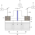
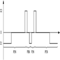
도 1a 및 도 1b는 본 발명의 제 1 실시예에 따른 전기-광학 변조 소자들의 단면들을 도시하는 단면도들이다. 도 1c는 본 발명의 제 1 실시예에 따른 전기-광학 변조 소자의 순-도핑 프로파일(net doping profile)을 설명하기 위한 그래프이다. 구체적으로, 도 1c는 도 1a 및 도 1b의 점선 I-I'을 따라 보여지는 순-도핑 프로파일을 도시하는 그래프이다. Figs. 1A and 1B are cross-sectional views showing cross-sections of electro-optic modulation elements according to a first embodiment of the present invention. 1C is a graph illustrating a net doping profile of the electro-optic modulation device according to the first embodiment of the present invention. Specifically, FIG. 1C is a graph showing the forward-doping profile along the dashed line I-I 'of FIGS. 1A and 1B.
도 1a 및 도 1b를 참조하면, 기판(10) 상에 광 도파로(WG)를 구성하는 반도체막(30)이 배치된다. 상기 광도파로(WG)는 제 1 슬랩 부분(SP1), 제 2 슬랩 부분(SP2) 및 이들 사이에 배치되는 립 부분(RP)을 포함하는 슬랩 도파로 구조일 수 있으며, 상기 립 부분(RP)은 상기 제 1 및 제 2 슬랩 부분들(SP1, SP2)보다 큰 두께로 형성될 수 있다. Referring to FIGS. 1A and 1B, a
본 발명의 일 실시예에 따르면, 상기 반도체막(30)은 단결정 실리콘으로 형성될 수 있다. 예를 들면, 상기 반도체막(30)은, 상기 기판(10)과 함께, 에스오아이 웨이퍼를 구성할 수 있다. 이 경우, 도시된 것처럼, 상기 기판(10)과 상기 반도체막(30) 사이에는 매몰 절연막(20)이 배치될 수 있다. 상기 매몰 절연막(20)은 상기 반도체막(30)보다 낮은 굴절률을 갖는 절연성 물질(예를 들면, 실리콘 산화막)으로 형성됨으로써, 상기 광 도파로(WG)의 클래드층으로 사용될 수 있다. 하지만, 본 발명의 기술적 사상이 이러한 웨이퍼 구조 또는 박막의 종류에 한정되는 것은 아니다. According to an embodiment of the present invention, the
상기 제 1 및 제 2 슬랩 부분들(SP1, SP2) 각각에는 제 1 및 제 2 도핑 영역들(D1, D2)이 형성될 수 있고, 상기 립 부분(RP)에는 수직 구조체를 구성하는 수직 도핑 영역(50)이 형성될 수 있다. 이 실시예에 따르면, 상기 제 1 및 제 2 도핑 영역들(D1, D2)은 제 1 도전형이고, 상기 수직 도핑 영역(50)은 상기 제 1 도전형과 다른 제 2 도전형일 수 있다. 예를 들면, 상기 제 1 및 제 2 도핑 영역들(D1, D2)이 p형일 경우, 상기 수직 도핑 영역(50)은 n형일 수 있다. 또는, 상기 제 1 및 제 2 도핑 영역들(D1, D2)이 n형일 경우, 상기 수직 도핑 영역(50)은 p형일 수 있다.The first and second doping regions D1 and D2 may be formed in the first and second slab portions SP1 and SP2 and the vertical doping region (50) may be formed. According to this embodiment, the first and second doped regions D1 and D2 may be of a first conductivity type and the vertical doped
또한, 이 실시예에 따르면, 상기 제 1 도핑 영역(D1)과 상기 수직 도핑 영역(50) 사이에 개재된 상기 광 도파로(WG)의 일 부분(이하, 제 1 몸체 영역(B1))은 상기 제 1 도핑 영역(D1)과 동일한 도전형(즉, 상기 제 1 도전형)일 수 있다. 즉, 상기 제 1 몸체 영역(B1)은 상기 수직 도핑 영역(50)과 다른 도전형으로 도핑될 수 있다. 이에 따라, 상기 제 1 몸체 영역(B1)과 상기 수직 도핑 영역(50)은 도 1c에 도시된 것처럼 피엔 접합(PN-junction)을 구성할 수 있다. 유사하게, 상기 제 2 도핑 영역(D2)과 상기 수직 도핑 영역(50) 사이에 개재된 상기 광 도파로(WG)의 다른 부분(이하, 제 2 몸체 영역(B2))은 상기 수직 도핑 영역(50)과 다른 도전형으로 도핑됨으로써, 상기 제 2 몸체 영역(B2)과 상기 수직 도핑 영역(50) 역시 피엔 접합을 구성할 수 있다. According to this embodiment, a part of the optical waveguide WG interposed between the first doped region D1 and the vertical doped region 50 (hereinafter referred to as a first body region B1) And may be of the same conductivity type as the first doped region D1 (i.e., the first conductive type). That is, the first body region B1 may be doped with a different conductivity type than that of the
도 1a를 참조하면, 상기 수직 도핑 영역(50)은 그 바닥면이 상기 매몰 절연막(20)의 상부면에 접촉하도록 형성될 수 있다. 즉, 상기 수직 도핑 영역(50)의 두께는 상기 립 부분(RP)의 두께와 실질적으로 동일할 수 있다. 이 경우, 도시된 것처럼, 상기 제 1 몸체 영역(B1)과 상기 제 2 몸체 영역(B2)은 상기 수직 도핑 영역(50)에 의해 서로 분리될 수 있다. 또한, 상기 수직 도핑 영역(50)은 상기 제 1 및 제 2 몸체 영역들(B1, B2)에 의해 정의되는 두 피엔 접합들의 공통 전극으로 사용될 수 있다. 본 발명의 다른 실시예에 따르면, 상기 제 1 몸체 영역(B1), 상기 수직 도핑 영역(50) 및 상기 제 2 몸체 영역(B2)은 바이폴라 접합 트랜지스터(BJT)를 구성할 수 있다. 이 경우, 상기 제 1 도핑 영역(D1)과 상기 제 2 도핑 영역(D2)은, 도시된 것과 달리, 서로 다른 전압을 생성하는 서로 다른 회로들에 접속될 수 있다. Referring to FIG. 1A, the vertical doped
도 1b를 참조하면, 상기 수직 도핑 영역(50)의 두께는 상기 립 부분(RP)의 두께보다 작을 수 있다. 이 경우, 도시된 것처럼, 상기 제 1 몸체 영역(B1)은 상기 수직 도핑 영역(50)의 아래에서 상기 제 2 몸체 영역(B2)에 연결될 수 있다. 즉, 상기 제 1 및 제 2 몸체 영역들(B1, B2)에 의해 구성되는 피엔 접합들은 상기 수직 도핑 영역(50) 아래에서 연결될 수 있다. 이 경우, (상기 립 부분(RP)의 진행 방향과 교차하는 소정의 평면 상에 투영되는) 상기 연결된 피엔 접합의 길이는 상기 수직 도핑 영역(50)의 길이의 두 배보다 길 수 있다. Referring to FIG. 1B, the thickness of the
한편, 도 1a 및 도 1b는 상기 광 도파로(WG)의 진행 방향을 가로지는 평면들 중의 하나에 투영된 전기-광학 변조 소자의 단면을 도시하는 단면도들일 뿐, 본 발명에 따른 전기-광학 변조 소자가 광 도파로 전체에 걸쳐 도시된 구조를 갖는다는 것을 보이기 위해 제공된 것이 아니다. 즉, 본 발명에 따른 전기-광학 변조 소자는 도면들에 도시된 단면 구조와 같이 형성되는 부분을 포함하지만, 그것의 모든 부분들이 도시된 단면 구조와 같이 형성될 필요는 없다. 예를 들면, 상기 광 도파로(WG)의 일부분에서, 상기 제 1 몸체 영역(B1)은 상기 제 2 몸체 영역(B2)에 직접 접촉하는 부분을 가질 수도 있다. 1A and 1B are sectional views showing a cross section of an electro-optic modulation element projected on one of the planes crossing the traveling direction of the optical waveguide WG, Is not provided to show that the optical waveguide has a structure shown throughout the optical waveguide. That is, the electro-optic modulation device according to the present invention includes a portion formed in the cross-sectional structure shown in the drawings, but not all portions of the electro-optic modulation device need to be formed with the cross-sectional structure shown. For example, in a portion of the optical waveguide WG, the first body region B1 may have a portion directly contacting the second body region B2.
이에 더하여, 상기 제 1 및 제 2 도핑 영역들(D1, D2)은 각각 상기 제 1 및 제 2 몸체 영역들(B1, B2)과 동일한 도전형이면서 이들보다 더 높은 농도로 도핑될 수 있다. 또한, 도 1c에 도시된 것처럼, 상기 수직 도핑 영역(50)은 상기 제 1 및 제 2 몸체 영역들(B1, B2)과 다른 도전형이면서 이들보다 더 높은 농도로 도핑될 수 있다. 비록, 도 1c에는, 어브럽트 접합 구조(abrupt junction structure)가 예시적으로 도시되었지만, 상기 수직 도핑 영역(50) 그리고 상기 제 1 및 제 2 몸체 영역들(B1, B2) 각각의 농도 프로파일은 다양하게 변형될 수 있다. 예를 들면, 상기 피엔 접합들은 선형적으로 경사진 접합 구조(linearly graded junction structure)로서 구현될 수도 있다. In addition, the first and second doped regions D1 and D2 may be doped with the same conductivity type and higher concentration than the first and second body regions B1 and B2, respectively. In addition, as shown in FIG. 1C, the vertical doped
이 실시예에 따르면, 상기 수직 도핑 영역(50)은 제 1 배선 구조체(91)를 이용하여 제 1 전압(V1)을 생성하는 제 1 회로(C1)에 전기적으로 연결되고, 상기 제 1 및 제 2 도핑 영역들(D1, D2)은 제 2 배선 구조체(92a, 92b)를 이용하여 제 2 전압(V2)을 생성하는 제 2 회로(C2)에 전기적으로 연결될 수 있다. According to this embodiment, the vertical doped
일 실시예에 따르면, 상기 제 1 전압(V1) 및 상기 제 2 전압(V2)은 각각 변조 전압 및 접지 전압일 수 있다. 이에 따라, 상기 수직 도핑 영역(50)과 상기 제 1 및 제 2 몸체부들(B1, B2) 사이에는, 상기 제 1 전압(V1)에 의해 결정되는, 소정의 전위 차가 생성될 수 있다. 상술한 것처럼, 상기 수직 도핑 영역(50)의 양쪽 측벽이 모두 피엔 접합을 구성하는데 이용되기 때문에, 도 1a 및 도 1b를 참조하여 설명된 실시예에 따른 전기-광학 변조 소자는, 종래 기술들에서 제안되었던 방식들에 비해, 증가된 유효 굴절률의 변화를 유발할 수 있다. 예를 들면, 이 실시예에 따른 전기-광학 변조 소자는 미국특허공개번호 제2006/0008223호에 개시된 방식에 비해 대략 2배의 유효 굴절률 변화를 유발할 수 있다. 유효 굴절률 변화에서의 이러한 증가는 증가된 위상 천이를 얻는 것을 가능하게 하거나, 광 도파로에서 변조 영역의 길이를 짧게 형성하는 것을 가능하게 한다. 특히, 상기 피엔 접합들이 피엔 역방향 모드(PN reverse mode)로 동작할 경우, 상기 광 도파로(WG)의 활성 영역을 높게 도핑해야 하는 기술적 문제를 경감시킬 수 있다. 즉, 이 실시예에 따르면, 상기 광 도파로(WG)의 평균 도핑 수준을 감소시키는 것이 가능하기 때문에, 상기 광 도파로(WG)에서의 광 손실은 경감될 수 있다. According to an embodiment, the first voltage V1 and the second voltage V2 may be a modulation voltage and a ground voltage, respectively. Accordingly, a predetermined potential difference, which is determined by the first voltage V1, may be generated between the vertical doped
[제 1 [First 변형예Variation example ]]
도 2a 및 도 2b는 본 발명의 제 1 변형예에 따른 전기-광학 변조 소자들의 단면들을 도시하는 단면도들이다. 도 2c는 본 발명의 제 1 변형예에 따른 전기-광학 변조 소자의 순-도핑 프로파일을 설명하기 위한 그래프이다. 구체적으로, 도 2c는 도 2a 및 도 2b의 점선 I-I'을 따라 보여지는 순-도핑 프로파일을 도시하는 그래프이다. 설명의 간결함을 위해, 도 1a 내지 도 1c를 참조하여 설명된 실시예들과 중복되는 기술적 특징들에 대한 설명은 생략될 수 있다. FIGS. 2A and 2B are cross-sectional views showing cross sections of electro-optic modulation elements according to a first modification of the present invention. FIG. 2C is a graph illustrating a forward-doping profile of an electro-optic modulation device according to a first modification of the present invention. FIG. Specifically, FIG. 2C is a graph showing the forward-doping profile along the dashed line I-I 'of FIGS. 2A and 2B. For brevity of description, the description of the technical features overlapping with the embodiments described with reference to Figs. 1A to 1C can be omitted.
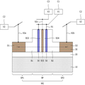
도 2a 및 도 2b를 참조하면, 이 실시예에 따르면, 상기 립 부분(RP)에는 두 개의 수직 도핑 영역들(50)을 포함하는 수직 구조체가 형성될 수 있다. 이에 더하여, 상기 수직 구조체는 상기 수직 도핑 영역들(50) 사이에 개재되는 내부 도핑 영역(B3)을 더 포함할 수 있다. Referring to FIGS. 2A and 2B, according to this embodiment, a vertical structure including two vertical
상기 내부 도핑 영역(B3)은 상기 제 1 및 제 2 몸체 영역들(B1, B2)과 같은 도전형이고, 상기 수직 도핑 영역들(50)은 상기 제 1 및 제 2 몸체 영역들(B1, B2)과 다른 도전형일 수 있다. 이에 따라, 상기 립 부분(RP)에는 도 1a 내지 도 1c를 참조하여 설명된 실시예에 비해 더욱 증가된 길이를 갖는 피엔 접합들이 형성될 수 있다. 예를 들면, 도 2a에 도시된 것처럼, 상기 수직 도핑 영역들(50)은 상기 매몰 절연막(20)의 상부면에 접하도록 형성됨으로써, 상기 수직 도핑 영역들(50) 각각은 분리된 두 개의 피엔 접합들의 공통 전극으로 이용될 수 있다. 즉, 도 2a의 실시예에 따르면, 도 2c에 도시된 것처럼, 상기 립 부분(RP)에는 네 개의 피엔 접합들이 형성될 수 있다. 또한, 도 2b에 도시된 것처럼, 상기 수직 도핑 영역들(50)은 상기 립 부분(RP)의 두께보다 얇게 형성됨으로써, 상기 수직 도핑 영역들(50)의 측면들 및 하부면들이 모두 피엔 접합을 구성하는데 이용될 수 있다. 이에 따라, 도 2b의 실시예에 따른 광학 장치의 피엔 접합의 길이는 도 1b의 실시예에 따른 광학 장치의 그것보다 대략 2배일 수 있다. The inner doping region B3 is of the same conductivity type as the first and second body regions B1 and B2 and the
한편, 도 2a 및 도 2b에 도시된 것처럼, 상기 수직 도핑 영역들(50)은 제 1 배선 구조체(91)를 이용하여 제 1 전압(V1)을 생성하는 제 1 회로(C1)에 전기적으로 연결될 수 있다. 일 실시예에 따르면, 도 2a에 도시된 것처럼, 상기 내부 도핑 영역(B1)은 내부 배선 구조체(92c)를 이용하여 제 2 전압(V2)을 생성하는 제 2 회로(C2)에 전기적으로 연결될 수 있다. 다른 실시예에 따르면, 도 2b에 도시된 것처럼, 상기 내부 도핑 영역(B3)이 상기 수직 도핑 영역들(50)의 하부에서 상기 제 1 및 제 2 몸체 영역들(B1, B2)과 전기적으로 연결됨으로써, 별도의 배선없이, 상기 제 1 및 제 2 몸체 영역들(B1, B2)과 등전위 상태에 있을 수 있다. 2A and 2B, the vertical
동작에 있어서, 상기 제 1 전압(V1) 및 상기 제 2 전압(V2)은 각각 변조 전압 및 접지 전압일 수 있다. 이에 따라, 상기 수직 도핑 영역들(50)과 상기 제 1 및 제 2 몸체부들(B1, B2) 사이에는, 상기 제 1 전압(V1)에 의해 결정되는, 소정의 전위 차가 생성될 수 있다. 일 실시예에 따르면, 상기 제 1 전압(V1) 및 상기 제 2 전압(V2)은 상기 피엔 접합들이 피엔 역방향 모드로 동작하도록 선택될 수 있다. In operation, the first voltage V1 and the second voltage V2 may be a modulation voltage and a ground voltage, respectively. Accordingly, a predetermined potential difference, which is determined by the first voltage V1, may be generated between the vertical
[제 2 [Second 변형예Variation example ]]
도 3a 및 도 3b는 본 발명의 제 2 변형예에 따른 전기-광학 변조 소자들의 단면들을 도시하는 단면도들이다. 도 3c는 본 발명의 제 2 변형예에 따른 전기-광학 변조 소자의 순-도핑 프로파일을 설명하기 위한 그래프이다. 구체적으로, 도 3c는 도 3a 및 도 3b의 점선 I-I'을 따라 보여지는 순-도핑 프로파일을 도시하는 그래프이다. 설명의 간결함을 위해, 도 1a 내지 도 1c를 참조하여 설명된 실시예들과 중복되는 기술적 특징들에 대한 설명은 생략될 수 있다. 3A and 3B are cross-sectional views showing cross-sections of electro-optic modulation elements according to a second modification of the present invention. FIG. 3C is a graph illustrating a forward-doping profile of an electro-optic modulation device according to a second modification of the present invention. FIG. Specifically, FIG. 3C is a graph showing the forward-doping profile along the dashed line I-I 'of FIGS. 3A and 3B. For brevity of description, the description of the technical features overlapping with the embodiments described with reference to Figs. 1A to 1C can be omitted.
도 3a 및 도 3b를 참조하면, 이 실시예에 따르면, 상기 립 부분(RP)에는 세 개의 수직 도핑 영역들(50)을 포함하는 수직 구조체가 형성될 수 있다. 이에 더하여, 상기 수직 구조체는 상기 수직 도핑 영역들(50) 사이에 개재되는 두 개의 내부 도핑 영역들(B31, B32)을 더 포함할 수 있다. Referring to FIGS. 3A and 3B, according to this embodiment, a vertical structure including three vertical
상기 내부 도핑 영역들(B31, B32)은 상기 제 1 및 제 2 몸체 영역들(B1, B2)과 같은 도전형이고, 상기 수직 도핑 영역들(50)은 상기 제 1 및 제 2 몸체 영역들(B1, B2)과 다른 도전형일 수 있다. 이에 따라, 상기 립 부분(RP)에는 도 2a 내지 도 2c를 참조하여 설명된 실시예에 비해 더욱 증가된 길이를 갖는 피엔 접합들이 형성될 수 있다. 예를 들면, 도 3a에 도시된 것처럼, 상기 수직 도핑 영역들(50)은 상기 매몰 절연막(20)의 상부면에 접하도록 형성됨으로써, 상기 수직 도핑 영역들(50) 각각은 분리된 두 개의 피엔 접합들의 공통 전극으로 이용될 수 있다. 즉, 도 3a의 실시예에 따르면, 도 3c에 도시된 것처럼, 상기 립 부분(RP)에는 여섯 개의 피엔 접합들이 형성될 수 있다. 또한, 도 3b에 도시된 것처럼, 상기 수직 도핑 영역들(50)은 상기 립 부분(RP)의 두께보다 얇게 형성됨으로써, 상기 수직 도핑 영역들(50)의 측면들 및 하부면들이 모두 피엔 접합을 구성하는데 이용될 수 있다. 이에 따라, 도 3b의 실시예에 따른 광학 장치의 피엔 접합의 길이는 도 1b의 실시예에 따른 광학 장치의 그것보다 대략 3배일 수 있다. The inner doping regions B31 and B32 are conductive types such as the first and second body regions B1 and B2 and the
한편, 도 3a 및 도 3b에 도시된 것처럼, 상기 수직 도핑 영역들(50)은 제 1 배선 구조체(91)를 이용하여 제 1 전압(V1)을 생성하는 제 1 회로(C1)에 전기적으로 연결될 수 있다. 일 실시예에 따르면, 도 3a에 도시된 것처럼, 상기 내부 도핑 영역들(B31, B32)은 내부 배선 구조체(92c)를 이용하여 제 2 전압(V2)을 생성하는 제 2 회로(C2)에 전기적으로 연결될 수 있다. 다른 실시예에 따르면, 도 3b에 도시된 것처럼, 상기 내부 도핑 영역(B31, B32)이 상기 수직 도핑 영역들(50)의 하부에서 상기 제 1 및 제 2 몸체 영역들(B1, B2)과 전기적으로 연결됨으로써, 별도의 배선없이, 상기 제 1 및 제 2 몸체 영역들(B1, B2)과 등전위 상태에 있을 수 있다. 3A and 3B, the vertical
동작에 있어서, 상기 제 1 전압(V1) 및 상기 제 2 전압(V2)은 각각 변조 전압 및 접지 전압일 수 있다. 이에 따라, 상기 수직 도핑 영역들(50)과 상기 제 1 및 제 2 몸체부들(B1, B2) 사이에는, 상기 제 1 전압(V1)에 의해 결정되는, 소정의 전위 차가 생성될 수 있다. 일 실시예에 따르면, 상기 제 1 전압(V1) 및 상기 제 2 전압(V2)은 상기 피엔 접합들이 피엔 역방향 모드로 동작하도록 선택될 수 있다. In operation, the first voltage V1 and the second voltage V2 may be a modulation voltage and a ground voltage, respectively. Accordingly, a predetermined potential difference, which is determined by the first voltage V1, may be generated between the vertical
[제 2 [Second 실시예Example ]]
도 4a는 본 발명의 제 2 실시예에 따른 전기-광학 변조 소자의 단면을 도시하는 단면도이다. 도 4b는 본 발명의 제 2 실시예에 따른 전기-광학 변조 소자의 순-도핑 프로파일(net doping profile)을 설명하기 위한 그래프이다. 구체적으로, 도 4b는 도 4a의 점선 I-I'을 따라 보여지는 순-도핑 프로파일을 도시하는 그래프이다. 설명의 간결함을 위해, 도 1a 내지 도 1c를 참조하여 설명된 실시예들과 중복되는 기술적 특징들에 대한 설명은 생략될 수 있다. 4A is a cross-sectional view illustrating an electro-optic modulation device according to a second embodiment of the present invention. 4B is a graph illustrating a net doping profile of the electro-optic modulation device according to the second embodiment of the present invention. Specifically, FIG. 4B is a graph showing the forward-doping profile along the dashed line I-I 'of FIG. 4A. For brevity of description, the description of the technical features overlapping with the embodiments described with reference to Figs. 1A to 1C can be omitted.
도 4a를 참조하면, 기판(10) 상에 광 도파로(WG)를 구성하는 반도체막(30)이 배치된다. 상기 광도파로(WG)는 제 1 슬랩 부분(SP1), 제 2 슬랩 부분(SP2) 및 이들 사이에 배치되는 립 부분(RP)을 포함할 수 있다. Referring to FIG. 4A, a
상기 제 1 및 제 2 슬랩 부분들(SP1, SP2) 각각에는 제 1 및 제 2 도핑 영역들(D1, D2)이 형성될 수 있고, 상기 립 부분(RP)에는 수직 구조체를 구성하는 수직 도핑 영역(50)이 형성될 수 있다. 이 실시예에 따르면, 상기 제 1 및 제 2 도핑 영역들(D1, D2)은 제 1 도전형이고, 상기 수직 도핑 영역(50)은 상기 제 1 도전형과 다른 제 2 도전형일 수 있다. 예를 들면, 상기 제 1 및 제 2 도핑 영역들(D1, D2)이 p형일 경우, 상기 수직 도핑 영역(50)은 n형일 수 있다. The first and second doping regions D1 and D2 may be formed in the first and second slab portions SP1 and SP2 and the vertical doping region (50) may be formed. According to this embodiment, the first and second doped regions D1 and D2 may be of a first conductivity type and the vertical doped
이 실시예에 따르면, 상기 제 1 도핑 영역(D1)과 상기 수직 도핑 영역(50) 사이에 개재된 상기 광 도파로(WG)의 일 부분(이하, 제 1 몸체 영역(B1))은 실질적으로 진성 반도체(intrinsic semiconductor)에 가까운 물성을 가질 수 있다. 예를 들면, 상기 제 1 몸체 영역(B1)은 언도프트 실리콘(undoped silicon) 또는 상기 제 1 도핑 영역(D1)보다 수 오더(order) 낮은 도핑 레벨을 갖는 실리콘일 수 있다. 이에 따라, 상기 제 1 도핑 영역(D1), 상기 제 1 몸체 영역(B1) 및 상기 수직 도핑 영역(50)은 도 4b에 도시된 것처럼 피아이엔 접합(PIN-junction)을 구성할 수 있다. 유사하게, 상기 제 2 도핑 영역(D2)과 상기 수직 도핑 영역(50) 사이에 개재된 상기 광 도파로(WG)의 다른 부분(이하, 제 2 몸체 영역(B2))은 실질적으로 진성 반도체에 가까운 물성을 가짐으로써, 상기 제 2 도핑 영역(D2), 상기 제 2 몸체 영역(B2) 및 상기 수직 도핑 영역(50) 역시 피아이엔 접합을 구성할 수 있다. According to this embodiment, a part of the optical waveguide WG interposed between the first doped region D1 and the vertical doped region 50 (hereinafter referred to as a first body region B1) It can have properties close to that of a semiconductor (intrinsic semiconductor). For example, the first body region B1 may be undoped silicon or silicon having a doping level that is orders of magnitude lower than the first doped region D1. Accordingly, the first doped region D1, the first body region B1, and the vertical doped
이에 더하여, 상기 수직 도핑 영역(50)은 그 바닥면이 상기 매몰 절연막(20)의 상부면에 접촉하도록 형성될 수 있다. 즉, 상기 수직 도핑 영역(50)의 두께는 상기 립 부분(RP)의 두께와 실질적으로 동일할 수 있다. 이 경우, 도시된 것처럼, 상기 제 1 몸체 영역(B1)과 상기 제 2 몸체 영역(B2)은 상기 수직 도핑 영역(50)에 의해 서로 분리됨으로써, 하나의 립 부분(RP) 내에는 두 개의 피아이엔 접합들이 형성될 수 있다. 상기 수직 도핑 영역(50)은 상기 제 1 및 제 2 몸체 영역들(B1, B2)에 의해 정의되는 두 피아이엔 접합들의 공통 전극으로 사용될 수 있다. In addition, the vertical doped
한편, 도 4a는 상기 광 도파로(WG)의 진행 방향을 가로지는 평면들 중의 하나에 투영된 전기-광학 변조 소자의 단면을 도시하는 단면도일 뿐, 본 발명에 따른 전기-광학 변조 소자가 광 도파로 전체에 걸쳐 도시된 구조를 갖는다는 것을 보이기 위해 제공된 것이 아니다. 즉, 본 발명에 따른 전기-광학 변조 소자는 도면들에 도시된 단면 구조와 같이 형성되는 부분을 포함하지만, 그것의 모든 부분들이 도시된 단면 구조와 같이 형성될 필요는 없다. 예를 들면, 상기 광 도파로(WG)의 변조 영역으로 사용되지 않는 부분에서, 상기 제 1 몸체 영역(B1)이 상기 제 2 몸체 영역(B2)에 직접 접촉하도록, 상기 수직 도핑 영역(50)이 형성되지 않을 수도 있다. 4A is a cross-sectional view showing an electro-optic modulation element projected on one of the planes crossing the traveling direction of the optical waveguide WG, and the electro-optic modulation element according to the present invention is an optical waveguide It is not intended to be seen as having a structure as shown throughout. That is, the electro-optic modulation device according to the present invention includes a portion formed in the cross-sectional structure shown in the drawings, but not all portions of the electro-optic modulation device need to be formed with the cross-sectional structure shown. For example, in the portion not used as a modulation region of the optical waveguide WG, the
이 실시예에 따르면, 상기 제 1 및 제 2 도핑 영역들(D1, D2)은 상기 매몰 절연막(20)의 상부면에 접하는 바닥면을 갖도록 형성될 수 있다. 즉, 상기 제 1 및 제 2 도핑 영역들(D1, D2)의 두께들은 상기 제 1 및 제 2 슬랩 부분들(SP1, SP2)의 그것들과 실질적으로 동일할 수 있다. 또한, 도 4b에는, 어브럽트 접합 구조(abrupt junction structure)가 예시적으로 도시되었지만, 상기 피아이엔 접합의 각 부분들의 농도 프로파일은 도시된 것으로부터 다양하게 변형되어 구현될 수 있다. According to this embodiment, the first and second doped regions D1 and D2 may be formed to have a bottom surface in contact with the upper surface of the embedded insulating
상기 수직 도핑 영역(50)은 제 1 배선 구조체(91)를 이용하여 제 1 전압(V1)을 생성하는 제 1 회로(C1)에 전기적으로 연결되고, 상기 제 1 및 제 2 도핑 영역들(D1, D2)은 제 2 배선 구조체(92a, 92b)를 이용하여 제 2 전압(V2)을 생성하는 제 2 회로(C2)에 전기적으로 연결될 수 있다. The
일 실시예에 따르면, 상기 제 1 전압(V1) 및 상기 제 2 전압(V2)은 각각 변조 전압 및 접지 전압일 수 있다. 이에 따라, 상기 수직 도핑 영역(50)과 상기 제 1 및 제 2 몸체부들(B1, B2) 사이에는, 상기 제 1 전압(V1)에 의존적인, 소정의 전위 차가 생성될 수 있다. 상술한 것처럼, 상기 수직 도핑 영역(50)의 양쪽 측벽이 모두 피아이엔 접합들을 구성하는데 이용되기 때문에, 도 4a를 참조하여 설명된 실시예에 따른 전기-광학 변조 소자는, 종래 기술들에서 제안되었던 방식들에 비해, 증가된 유효 굴절률의 변화를 유발할 수 있다. 유효 굴절률 변화에서의 이러한 증가는 증가된 위상 천이를 얻는 것을 가능하게 하거나, 광 도파로에서 변조 영역의 길이를 짧게 형성하는 것을 가능하게 한다. 특히, 상기 피아이엔 접합들이 피아이엔 순방향 모드로 동작하도록 상기 제 1 및 제 2 전압들(V1, V2)이 생성될 경우, 상기 광 도파로로 주입되는 전류의 크기는 종래 기술의 경우에 비해 두 배로 증가될 수 있다. 달리 말해, 이 실시예에 따른 전기-광학 변조 소자는 종래 기술에서보다 낮은 변조 전압으로 더 높은 효율의 위상 천이를 구현하는 것을 가능하게 한다. 이에 더하여, 상기 수직 도핑 영역(50)의 폭을 소정의 크기 이하로 유지시킬 경우, 고농도로 도핑된 상기 수직 도핑 영역(50)에 의해 야기될 수 있는 광 손실의 문제는 억제될 수 있다. According to an embodiment, the first voltage V1 and the second voltage V2 may be a modulation voltage and a ground voltage, respectively. A predetermined potential difference depending on the first voltage V1 may be generated between the vertical doped
[제 3 [Third 변형예Variation example ]]
도 5a는 본 발명의 제 3 변형예에 따른 전기-광학 변조 소자들의 단면들을 도시하는 단면도이다. 도 5b는 본 발명의 제 3 변형예에 따른 전기-광학 변조 소자의 순-도핑 프로파일을 설명하기 위한 그래프이다. 구체적으로, 도 5b는 도 5a의 점선 I-I'을 따라 보여지는 순-도핑 프로파일을 도시하는 그래프이다. 설명의 간결함을 위해, 도 4a 및 도 4b를 참조하여 설명된 실시예들과 중복되는 기술적 특징들에 대한 설명은 생략될 수 있다. 5A is a cross-sectional view showing cross sections of electro-optic modulation elements according to a third modification of the present invention. FIG. 5B is a graph illustrating a forward-doping profile of an electro-optic modulation device according to a third modification of the present invention. FIG. Specifically, FIG. 5B is a graph showing the forward-doping profile along the dashed line I-I 'of FIG. 5A. For brevity of description, the description of the technical features overlapping with the embodiments described with reference to Figs. 4A and 4B can be omitted.
도 5a를 참조하면, 이 실시예에 따르면, 상기 립 부분(RP)에는 두 개의 수직 도핑 영역들(50)을 포함하는 수직 구조체가 형성될 수 있다. 이에 더하여, 상기 수직 구조체는 상기 수직 도핑 영역들(50) 사이에 개재되는 한 쌍의 진성 영역들(B33, B34) 및 상기 진성 영역들(B33, B34) 사이에 개재되는 하나의 내부 도핑 영역(B35)을 더 포함할 수 있다. Referring to FIG. 5A, according to this embodiment, a vertical structure including two vertical
상기 진성 영역들(B33, B34)은, 상기 제 1 및 제 2 몸체 영역들(B1, B2)과 동일하게, 진성 반도체(intrinsic semiconductor)에 가까운 물성을 가질 수 있다. 하지만, 상기 진성 영역들(B33, B34)과 상기 제 1 및 제 2 몸체 영역들(B1, B2)은 완전하게 동일한 물성을 가질 필요는 없다. The intrinsic regions B33 and B34 may have physical properties similar to intrinsic semiconductors as the first and second body regions B1 and B2. However, it is not necessary that the intrinsic regions B33 and B34 and the first and second body regions B1 and B2 have completely the same physical properties.
상기 내부 도핑 영역(B35)은 상기 제 1 및 제 2 도핑 영역들(D1, D2)과 같은 도전형을 가질 수 있다. 즉, 상기 내부 도핑 영역(B35)은 상기 수직 도핑 영역들(50)과 다른 도전형을 갖게 되어, 도 5b에 도시된 것처럼, 상기 수직 구조체의 내부에는 한 쌍의 피아이엔 접합들이 형성될 수 있다. 결과적으로, 상기 광 도파로(WG)는, 상기 제 1 및 제 2 몸체 영역들(B1, B2) 그리고 상기 제 1 및 제 2 진성 영역들(B33, B34) 각각을 진성 반도체로 사용하는, 네 개의 피아이엔 접합들을 포함할 수 있다. 이에 따라, 이 실시예는 도 4a를 참조하여 설명된 실시예에 비해 더욱 증가된 길이를 갖는 피아이엔 접합들을 포함할 수 있다. The inner doped region B35 may have the same conductivity type as the first and second doped regions D1 and D2. That is, the inner doped region B35 has a different conductivity type from the vertical
한편, 도 5a에 도시된 것처럼, 상기 수직 도핑 영역들(50)은 제 1 배선 구조체(91)를 이용하여 제 1 전압(V1)을 생성하는 제 1 회로(C1)에 전기적으로 연결되고, 상기 내부 도핑 영역(B35)은 내부 배선 구조체(92c)를 이용하여 제 2 전압(V2)을 생성하는 제 2 회로(C2)에 전기적으로 연결될 수 있다. 5A, the vertical
일 실시예에 따르면, 상기 제 1 전압(V1) 및 상기 제 2 전압(V2)은 각각 변조 전압 및 접지 전압일 수 있다. 이에 따라, 상기 수직 도핑 영역(50)과 상기 제 1 및 제 2 몸체부들(B1, B2) 사이에는, 상기 제 1 전압(V1)에 의존적인, 소정의 전위 차가 생성될 수 있다. 특히, 상기 제 1 및 제 2 전압들(V1, V2)이 상기 피아이엔 접합들이 피아이엔 순방향 모드로 동작하도록 생성될 경우, 상기 광 도파로로 주입되는 전류의 크기는 종래 기술 또는 도 4a를 참조하여 설명된 실시예에 비해 더욱 증가될 수 있다. 앞선 실시예들에서와 유사하게, 상기 수직 도핑 영역들(50)의 폭을 소정의 크기 이하로 유지시킬 경우, 고농도로 도핑된 상기 수직 도핑 영역들(50)에 의해 야기될 수 있는 광 손실의 문제는 억제될 수 있다. According to an embodiment, the first voltage V1 and the second voltage V2 may be a modulation voltage and a ground voltage, respectively. A predetermined potential difference depending on the first voltage V1 may be generated between the vertical doped
[제 4 [Fourth 변형예Variation example ]]
도 6a 및 도 6b는 본 발명의 제 4 변형예에 따른 전기-광학 변조 소자들의 단면들을 도시하는 단면도들이다. 도 6c는 본 발명의 제 4 변형예에 따른 전기-광학 변조 소자의 순-도핑 프로파일을 설명하기 위한 그래프이다. 구체적으로, 도 6c는 도 6a 및 도 6b의 점선 I-I'을 따라 보여지는 순-도핑 프로파일을 도시하는 그래프이다. 설명의 간결함을 위해, 도 4a 및 도 4b를 참조하여 설명된 실시예들과 중복되는 기술적 특징들에 대한 설명은 생략될 수 있다. 6A and 6B are cross-sectional views showing cross sections of electro-optic modulation elements according to a fourth modification of the present invention. FIG. 6C is a graph illustrating a forward-doping profile of an electro-optic modulation device according to a fourth modification of the present invention. FIG. Specifically, FIG. 6C is a graph showing the forward-doping profile along the dashed line I-I 'of FIGS. 6A and 6B. For brevity of description, the description of the technical features overlapping with the embodiments described with reference to Figs. 4A and 4B can be omitted.
도 6a 및 도 6b를 참조하면, 이 실시예에 따르면, 상기 립 부분(RP)에는 두 개의 수직 도핑 영역들(50) 및 상기 수직 도핑 영역들(50) 사이에 개재되는 하나의 내부 도핑 영역(B35)을 포함하는 수직 구조체가 형성될 수 있다. 6A and 6B, according to this embodiment, the lip portion RP includes two
상기 내부 도핑 영역(B35)은 상기 제 1 및 제 2 도핑 영역들(D1, D2)과 같은 도전형을 가질 수 있다. 즉, 상기 내부 도핑 영역(B35)은 상기 수직 도핑 영역들(50)과 다른 도전형을 갖게 되어, 도 6c에 도시된 것처럼, 상기 수직 구조체의 내부에는 한 쌍의 피엔 접합들이 형성될 수 있다. 결과적으로, 상기 광 도파로(WG)는 두 개의 피아이엔 접합들 및 두 개의 피엔 접합들을 포함할 수 있다. The inner doped region B35 may have the same conductivity type as the first and second doped regions D1 and D2. That is, the inner doped region B35 has a different conductivity type from that of the vertical
일 실시예에 따르면, 상기 수직 도핑 영역들(50)은, 도 6a에 도시된 것처럼, 제 1 배선 구조체(91)를 이용하여 제 1 전압(V1)을 생성하는 제 1 회로(C1)에 전기적으로 연결되고, 상기 내부 도핑 영역(B35)은 내부 배선 구조체(92c)를 이용하여 제 2 전압(V2)을 생성하는 제 2 회로(C2)에 전기적으로 연결될 수 있다. 이 실시예에 따르면, 상기 수직 도핑 영역들(50)과 상기 제 1 및 제 2 도핑 영역들(D1, D2) 사이에는 순방향의 직류 전압이 인가됨으로써 상기 피아이엔 접합들은 피아이엔 순방향 모드(PIN forward mode)로 동작될 수 있다. 또한, 상기 수직 도핑 영역들(50)과 상기 내부 도핑 영역(B35) 사이에는 역방향의 직류 전압이 인가됨으로써, 상기 피엔 접합들은 피엔 역방향 모드(PN Reverse mode)로 동작될 수 있다. 결과적으로, 이 실시예에 따른 전기-광학 변조 소자는, 굴절률의 변화를 유발하는 두가지 효과들이 함께 발생하는, 혼합 구조(hybrid structure)일 수 있다. 이러한 효과들 중의 한가지는 피아이엔 순방향 모드로 동작하는 두 개의 피아이엔 접합의 전류 주입 효과에 따른 굴절률 변화이고, 다른 하나는 피엔 역방향 모드로 동작하는 두 개의 피엔 접합들에서의 공핍층 변화에 따른 굴절률 변화이다. According to one embodiment, the vertical
다른 실시예에 따르면, 도 6b에 도시된 것처럼, 상기 수직 도핑 영역들(50)은 제 1 배선 구조체(91)를 이용하여 제 1 전압(V1)을 생성하는 제 1 회로(C1)에 전기적으로 연결되고, 상기 내부 도핑 영역(B35)은 외부 회로와 전기적으로 연결되지 않은 상태에 있을 수 있다. 이 실시예에 따르면, 상기 수직 도핑 영역들(50)과 상기 제 1 및 제 2 도핑 영역들(D1, D2) 사이에는 순방향의 직류 전압이 인가됨으로써 상기 피아이엔 접합들은 피아이엔 순방향 모드(PIN forward mode)로 동작될 수 있다. 하지만, 상기 내부 도핑 영역(B35)은 전기적으로 부유(floating) 상태에 있을 수 있다.
6B, the vertical
[제 5 [Fifth 변형예Variation example ]]
도 7a는 본 발명의 제 5 변형예에 따른 전기-광학 변조 소자들의 단면들을 도시하는 단면도이다. 도 7b는 본 발명의 제 5 변형예에 따른 전기-광학 변조 소자의 순-도핑 프로파일을 설명하기 위한 그래프이다. 구체적으로, 도 7b는 도 7a의 점선 I-I'을 따라 보여지는 순-도핑 프로파일을 도시하는 그래프이다. 설명의 간결함을 위해, 앞선 도면들을 참조하여 설명된 실시예들과 중복되는 기술적 특징들에 대한 설명은 생략될 수 있다. 7A is a cross-sectional view showing cross sections of electro-optic modulation elements according to a fifth modification of the present invention. FIG. 7B is a graph illustrating a forward-doping profile of an electro-optic modulation device according to a fifth modification of the present invention. Specifically, FIG. 7B is a graph showing the forward-doping profile along the dashed line I-I 'of FIG. 7A. For brevity of description, the description of the technical features overlapping with the embodiments described with reference to the preceding drawings may be omitted.
도 7a를 참조하면, 이 실시예에 따르면, 상기 립 부분(RP)에는 세 개의 수직 도핑 영역들(50) 및 상기 수직 도핑 영역들(50) 사이에 개재되는 한 쌍의 내부 도핑 영역들(B36, B37)을 포함하는 수직 구조체가 형성될 수 있다. Referring to FIG. 7A, according to this embodiment, the lip portion RP includes three
상기 내부 도핑 영역들(B36, B37)은 상기 제 1 및 제 2 도핑 영역들(D1, D2)과 같은 도전형을 가질 수 있다. 즉, 상기 내부 도핑 영역들(B36, B37)은 상기 수직 도핑 영역들(50)과 다른 도전형을 가지며, 그 결과로서, 도 7b에 도시된 것처럼, 상기 수직 구조체의 내부에는 네 개의 피엔 접합들이 형성될 수 있다. 결과적으로, 상기 광 도파로(WG)는 상기 제 1 및 제 2 몸체 영역들(B1, B2)을 이용하여 구현되는 두 개의 피아이엔 접합들 및 상기 수직 구조체 내부에 구현되는 네 개의 피엔 접합들을 포함할 수 있다. The internal doped regions B36 and B37 may have the same conductivity type as the first and second doped regions D1 and D2. That is, the inner doped regions B36 and B37 have different conductivity types from those of the vertical
상기 수직 도핑 영역들(50)은, 도 7a에 도시된 것처럼, 제 1 배선 구조체(91)를 이용하여 제 1 전압(V1)을 생성하는 제 1 회로(C1)에 전기적으로 연결되고, 상기 내부 도핑 영역들(B36, B37)은 내부 배선 구조체(92c)를 이용하여 제 2 전압(V2)을 생성하는 제 2 회로(C2)에 전기적으로 연결될 수 있다. 이 실시예에 따르면, 상기 수직 도핑 영역들(50)과 상기 제 1 및 제 2 도핑 영역들(D1, D2) 사이에는 순방향의 직류 전압이 인가됨으로써 상기 피아이엔 접합들은 피아이엔 순방향 모드(PIN forward mode)로 동작될 수 있다. 또한, 상기 수직 도핑 영역들(50)과 상기 내부 도핑 영역들(B36, B37) 사이에는 역방향의 직류 전압이 인가됨으로써, 상기 피엔 접합들은 피엔 역방향 모드(PN Reverse mode)로 동작될 수 있다. 결과적으로, 이 실시예에 따른 전기-광학 변조 소자 역시 도 6a를 참조하여 설명된 혼합 구조(hybrid structure)의 하나일 수 있다. 즉, 이 실시예에 따른 전기-광학 변조 소자는 피아이엔 순방향 모드로 동작하는 두 개의 피아이엔 접합들에서의 전류 주입 효과에 따른 굴절률 변화 효과 및 피엔 역방향 모드로 동작하는 네 개의 피엔 접합들에서의 공핍층 변화에 따른 굴절률 변화 효과를 동시에 구현할 수 있다. The vertical
[제 6 [Sixth 변형예Variation example ]]
도 8a 내지 도 8c는 본 발명의 제 6 변형예에 따른 전기-광학 변조 소자들의 단면들을 도시하는 단면도들이다. 구체적으로, 도 8a 내지 도 8c는 각각 도 5a, 도 6a 및 도 7a을 참조하여 설명된 실시예들로부터 변형된 실시예들에 관한 것으로, 설명의 간결함을 위해, 앞선 도면들을 참조하여 설명된 실시예들과 중복되는 기술적 특징들에 대한 설명은 생략될 수 있다. 8A to 8C are cross-sectional views showing cross sections of electro-optic modulation elements according to a sixth modification of the present invention. Specifically, Figs. 8A to 8C relate to embodiments modified from the embodiments described with reference to Figs. 5A, 6A and 7A, respectively, and for the sake of brevity of description, Descriptions of the technical features overlapping with the examples may be omitted.
도 8a 내지 도 8c를 참조하면, 상기 수직 구조체 내부의 내부 도핑 영역들(즉, 도 8a 및 도 8b의 B35, 도 8c의 B36 및 B37)은 제 3 전압(V3)을 생성하는 제 3 회로(C3)에 전기적으로 연결될 수 있다. 이 경우, 상기 제 3 전압(V3)은 상기 제 1 및 제 2 도핑 영역들(D1, D2)에 인가되는 전압인 상기 제 2 전압(V2)과 다를 수 있다. 이에 따라, 상기 수직 구조체의 내부에 형성되는 도 8a의 피아이엔 접합들 또는 도 8b 및 도 8c의 피엔 접합들은 상기 수직 구조체의 외부에 형성되는 피아이엔 접합들과 독립적으로 동작될 수 있다. 8A to 8C, internal doping regions (i.e., B35 in FIGS. 8A and 8B and B36 and B37 in FIG. 8C) within the vertical structure are connected to a third circuit C3. ≪ / RTI > In this case, the third voltage V3 may be different from the second voltage V2, which is a voltage applied to the first and second doped regions D1 and D2. Accordingly, the pi-ene junctions of Fig. 8a or the pien junctions of Figs. 8b and 8c formed inside the vertical structure can be operated independently of the pi-ene junctions formed outside the vertical structure.
구체적으로, 일 실시예에 따르면, 상기 수직 도핑 영역들(50)과 상기 제 1 및 제 2 도핑 영역들(D1, D2) 사이에는 순방향의 직류 전압이 인가됨으로써, 상기 수직 구조체의 외부에 형성되는 상기 피아이엔 접합들은 피아이엔 순방향 모드(PIN forward mode)로 동작될 수 있다. 하지만, 상기 수직 도핑 영역들(50)과 상기 내부 도핑 영역들(B36, B37) 사이에는 인가되는 전위 차는 상기 제 2 전압(V2)과 다른 상기 제 3 전압(V3)에 의해 결정될 수 있기 때문에, 상기 수직 구조체 내부의 접합들은 상기 수직 구조체 외부의 피아이엔 접합들의 동작과는 무관하게 최적화된 조건 아래에서 동작될 수 있다. 결과적으로, 상기 수직 구조체의 내부 및 외부의 접합들은 서로 독립적으로 최적화된 조건 아래에서 동작될 수 있으며, 이러한 독립적인 최적화는 이 실시예에 따른 전기-광학 변조 소자에서의 변조 특성을 향상시키는데 이용될 수 있다. Specifically, according to one embodiment, forward DC voltage is applied between the
[제 3 [Third 실시예Example ]]
도 9a 및 도 9b는 본 발명의 제 3 실시예에 따른 전기-광학 변조 소자들의 단면들을 도시하는 단면도들이다. 설명의 간결함을 위해, 앞서 설명된 실시예들과 중복되는 기술적 특징들에 대한 설명은 생략될 수 있다. Figs. 9A and 9B are cross-sectional views showing cross sections of electro-optic modulation elements according to a third embodiment of the present invention. For brevity of description, the description of the technical features overlapping with the above-described embodiments may be omitted.
도 9a 및 도 9b를 참조하면, 기판(10) 상에 광 도파로(WG)를 구성하는 반도체막(30)이 배치된다. 상기 광도파로(WG)는 제 1 슬랩 부분(SP1), 제 2 슬랩 부분(SP2) 및 이들 사이에 배치되는 립 부분(RP)을 포함할 수 있다. 9A and 9B, a
상기 제 1 및 제 2 슬랩 부분들(SP1, SP2) 각각에는 제 1 및 제 2 도핑 영역들(D1, D2)이 형성될 수 있고, 상기 립 부분(RP)에는 수직 구조체가 형성될 수 있다. 이 실시예에 따르면, 상기 제 1 도핑 영역(D1) 및 제 2 도핑 영역(D2)은 서로 다른 도전형들을 가질 수 있다. 예를 들면, 상기 제 1 도핑 영역(D1)은 p형이고, 상기 제 2 도핑 영역(D2)은 n형일 수 있다. 이에 따라, 상기 제 1 및 제 2 슬랩 부분들(SP1, SP2)은 상기 립 부분(RP)을 기준으로 하는 도핑 프로파일의 측면에서 비대칭적일 수 있다. First and second doped regions D1 and D2 may be formed in each of the first and second slab portions SP1 and SP2 and a vertical structure may be formed in the lip portion RP. According to this embodiment, the first doped region D1 and the second doped region D2 may have different conductivity types. For example, the first doped region D1 may be p-type and the second doped region D2 may be n-type. Accordingly, the first and second slab portions SP1, SP2 may be asymmetric in terms of the doping profile with respect to the lip portion RP.
상기 수직 구조체는 서로 이격된 제 1 수직 도핑 영역(51) 및 제 2 수직 도핑 영역(52), 그리고 이들 사이에 개재되는 내부 영역(B3)을 포함할 수 있다. 상기 제 1 수직 도핑 영역(51)과 상기 제 2 수직 도핑 영역(52)은 서로 다른 도전형이고, 상기 내부 영역(B3)은 진성 반도체일 수 있다. 이에 따라, 상기 수직 구조체 내부에 형성된, 상기 제 1 수직 도핑 영역(51), 상기 제 2 수직 도핑 영역(52) 및 상기 내부 영역(B3)은 하나의 피아이엔 접합을 구성할 수 있다. The vertical structure may include a first vertical doped
이에 더하여, 상기 제 1 수직 도핑 영역(51)은 상기 제 1 도핑 영역(D1)과 다른 도전형을 가지면서 상기 제 1 도핑 영역(D1)에 인접하게 형성되고, 상기 제 2 수직 도핑 영역(52)은 상기 제 2 도핑 영역(D2)과 다른 도전형을 가지면서 상기 제 2 도핑 영역(D2)에 인접하게 형성될 수 있다. 상기 제 1 수직 도핑 영역(51)과 상기 제 1 도핑 영역(D1) 사이에 배치되는 제 1 몸체 영역(B1) 및 상기 제 2 수직 도핑 영역(52)과 상기 제 2 도핑 영역(D2) 사이에 배치되는 제 2 몸체 영역(B2)은 진성 반도체일 수 있다. 이 경우, 상기 제 1 수직 도핑 영역(51), 상기 제 1 몸체 영역(B1) 및 상기 제 1 도핑 영역(D1)은 하나의 피아이엔 접합을 구성하고, 상기 제 2 수직 도핑 영역(52), 상기 제 2 몸체 영역(B2) 및 상기 제 2 도핑 영역(D2)은 또다른 피아이엔 접합을 구성할 수 있다. In addition, the first vertical doped
상기 제 1 및 제 2 수직 도핑 영역들(51, 52)은 도 9b에 도시된 것처럼 상기 립 부분(RP)의 두께보다 짧은 깊이까지 형성되거나, 도 9a에 도시된 것처럼 상기 매몰 절연막(20)의 상부면까지 연장될 수 있다. The first and second vertical
상기 제 1 수직 도핑 영역(51) 및 상기 제 2 도핑 영역(D2)은 제 1 배선 구조체(91)를 이용하여 제 1 전압(V1)을 생성하는 제 1 회로(C1)에 전기적으로 연결되고, 상기 제 2 수직 도핑 영역(52) 및 상기 제 1 도핑 영역(D1)은 제 2 배선 구조체(92)를 이용하여 제 2 전압(V2)을 생성하는 제 2 회로(C2)에 전기적으로 연결될 수 있다. 일 실시예에 따르면, 상기 제 1 전압(V1) 및 상기 제 2 전압(V2)은 각각 변조 전압 및 접지 전압일 수 있다. 또한, 상기 제 1 및 제 2 회로들(C1, C2)은 상기 피아이엔 접합들이 피아이엔 순방향 모드로 동작하도록 상기 제 1 및 제 2 전압들(V1, V2)을 생성할 수 있다.
The first
[제 4 [Fourth 실시예Example ]]
도 10a 및 도 10b는 본 발명의 제 4 실시예에 따른 전기-광학 변조 소자들의 단면들을 도시하는 단면도들이다. 설명의 간결함을 위해, 앞서 설명된 실시예들과 중복되는 기술적 특징들에 대한 설명은 생략될 수 있다. 10A and 10B are cross-sectional views showing cross-sections of electro-optic modulation elements according to a fourth embodiment of the present invention. For brevity of description, the description of the technical features overlapping with the above-described embodiments may be omitted.
도 10a 및 도 10b를 참조하면, 기판(10) 상에 광 도파로(WG)를 구성하는 반도체막(30)이 배치된다. 상기 광도파로(WG)는 상기 매몰 절연막(20)의 상부면을 노출시키는 측벽들을 갖도록 형성될 수 있다. 즉, 이 실시예에 따르면, 상기 광도파로(WG)는 채널 도파로 구조로 형성될 수 있다. Referring to FIGS. 10A and 10B, a
상기 광 도파로(WG) 내에는 적어도 한 쌍의 수직 도핑 영역들(50)을 갖는 수직 구조체가 형성될 수 있다. 상기 수직 구조체는 상기 수직 도핑 영역들(50) 사이에 개재되는 내부 도핑 영역(B35) 및 상기 내부 도핑 영역(B35)과 상기 수직 도핑 영역들(50) 사이에 개재되는 적어도 두 개의 내부 영역들(B36, B37)을 더 포함할 수 있다. 상기 내부 도핑 영역(B35)은 상기 수직 도핑 영역들(50)과 다른 도전형을 가질 수 있다. 상기 내부 영역들(B36, B37)은 도 10a에 도시된 것처럼 소정의 불순물로 도핑되거나 도 10b에 도시된 것처럼 진성 반도체일 수 있다. A vertical structure having at least one pair of vertical
상기 내부 영역들(B36, B37)이 도핑되는 경우에 있어서, 도 10a에 도시된 것처럼, 상기 내부 영역들(B36, B37)은 불순물 농도에서는 상기 내부 도핑 영역(B35)보다 낮고, 도전형에서는 상기 내부 도핑 영역(B35)과 같을 수 있다. 이러한 실시예에 따르면, 상기 내부 영역들(B36, B37)과 상기 수직 도핑 영역들(50)은 한 쌍의 피엔 접합들을 구성할 수 있다. 변형된 실시예에 따르면, 상기 내부 영역(B36, B37)은 불순물 농도에서는 상기 수직 도핑 영역(50)보다 낮고 도전형에서는 상기 수직 도핑 영역(50)과 같을 수 있다. 마찬가지로, 이러한 변형된 실시예에 따르면, 상기 내부 영역들(B36, B37)과 상기 내부 도핑 영역(B35)은 한 쌍의 피엔 접합들을 구성할 수 있다. In the case where the internal regions B36 and B37 are doped, the internal regions B36 and B37 are lower than the internal doping region B35 at the impurity concentration, And may be the same as the internal doping region B35. According to this embodiment, the inner regions B36 and B37 and the
상기 내부 영역들(B36, B37)이 진성 반도체인 경우, 도 10b에 도시된 것처럼, 상기 수직 도핑 영역들(50), 상기 내부 영역들(B36, B37) 및 상기 내부 도핑 영역(B35)은 한 쌍의 피아이엔 접합들을 구성할 수 있다. 10B, the
상기 수직 도핑 영역들(50)은 제 1 배선 구조체(91)를 이용하여 제 1 전압(V1)을 생성하는 제 1 회로(C1)에 전기적으로 연결되고, 상기 내부 도핑 영역(B35)은 제 2 배선 구조체(92)를 이용하여 제 2 전압(V2)을 생성하는 제 2 회로(C2)에 전기적으로 연결될 수 있다. 상기 제 1 전압(V1) 및 상기 제 2 전압(V2)은 각각 변조 전압 및 접지 전압일 수 있다. 도 10a를 참조하여 설명된 실시예의 경우, 상기 제 1 및 제 2 회로들(C1, C2)은 상기 피엔 접합들이 피엔 역방향 모드로 동작하도록 상기 제 1 및 제 2 전압들(V1, V2)을 생성할 수 있다. 도 10b를 참조하여 설명된 실시예의 경우, 상기 제 1 및 제 2 회로들(C1, C2)은 상기 피아이엔 접합들이 피아이엔 순방향 모드로 동작하도록 상기 제 1 및 제 2 전압들(V1, V2)을 생성할 수 있다.
The vertical
도 11은 본 발명의 실시예들에 따른 광 송신기 및 광 수신기를 포함하는 광학 시스템의 일 실시예를 개략적으로 도시하는 블록 다이어그램이다. 11 is a block diagram schematically illustrating an embodiment of an optical system including an optical transmitter and an optical receiver according to embodiments of the present invention.
도 11을 참조하면, 광학 시스템(optical system; 1001)은 적어도 하나의 광 송신기(optical transmitter; 1002) 및 적어도 하나의 광 수신기(optical receiver; 1006)를 포함한다. 상기 광학 시스템(1001)은 상기 광 송신기(1002) 및 상기 광 수신기(1006) 사이에 광학적으로 결합된 광학 장치(optical device; 1004)를 포함할 수 있다. 상기 광 송신기(1002)는, 상기 광학 장치(1004)에서 수신되는, 광학 빔(optical beam, 1010)을 전송하도록 구성될 수 있다. 상기 광학 장치(1004)는 변조 신호(modulating signal)(V1)에 응답하여 상기 광학 빔(1010)의 광학적 특성들 중의 하나를 변조시키도록 구성될 수 있다. 예를 들면, 상기 광학 장치(1004)는 도 1 내지 도 10을 참조하여 설명된 전기-광학 변조 소자들 중의 하나를 포함할 수 있다. 일 실시예에 따르면, 상기 광학 장치(1004)는 광 지연 소자(optical delay)로서 기능하도록 구성될 수도 있다. 다른 실시예에 따르면, 상기 광학 장치(1004)는 광 진폭 변조기(optical amplitude modulator) 등을 구현하기 위해 사용될 수 있다. Referring to FIG. 11, an
도 12는 도 11의 상기 광학 장치(1004)로서 채용될 수 있는 광 변조기(1100)의 일 실시예를 도시하는 도면들이다. FIG. 12 is a diagram illustrating an embodiment of an
도 12를 참조하면, 상기 광 변조기(1100)는 마흐-젠더 간섭계 구조(Mach-Zehnder Interferometer configuration)(MZI)의 두 Y-가지 커플러들(cascaded Y-branch couplers) 사이에 광학적으로 결합된 두 암들(arms) 중의 하나에 형성된 광위상 천이기(optical phase shifter)(1110)를 포함할 수 있다. 일 실시예에 따르면, 상기 광위상 천이기(1110)는 도 1 내지 10를 참조하여 설명된 전기-광학 변조기들 중의 하나 또는 이와 유사한 구조를 갖도록 형성될 수 있다. 12, the
동작에 있어서, 광학 빔(1010)은 상기 MZI의 입력 부분으로 입사된 후, 첫번째 Y-가지 커플러에서 분리된다. 그 결과, 상기 광학 빔(1010)의 제 1 부분은 MZI의 암들 중의 하나로 진행하고 상기 광학 빔(1010)의 제 2 부분은 MZI의 암들 중의 다른 하나로 진행한다. 도시된 것처럼, 상기 MZI의 암들 중의 하나에는 상기 광위상 천이기(1110)가 형성되어, 외부 신호(V1, V2)에 응답하여 상기 광학 빔(1010)의 제 1 및 제 2 부분들 사이의 상대 위상차(a relative phase difference)를 조절한다. 상기 광학 빔(1010)의 제 1 및 제 2 부분들은 상기 MZI의 출력 부분에서 합쳐진다. 상기 상대 위상차에 의한 상기 광학 빔(1010)의 제 1 및 제 2 부분들 사이의 보강 간섭 또는 소멸 간섭의 결과로서, 상기 MZI의 출력 부분으로부터 방출되는 상기 광학 빔(1010)은 변조된 특성을 가질 수 있다. 일 실시예에 따르면, 상기 MZI의 입력 부분으로 입사되는 상기 광학 빔(1010)은 연속파(continuous wave)일 수 있고, 상기 MZI의 출력 부분으로부터 방출되는 상기 광학 빔(1010)은 상기 변조의 결과로서 톱니 모양의 파형을 가질 수 있다. 본 발명의 변형된 실시예에 따르면, 상기 MZI의 두 암들 모두 본 발명이 개시하는 전기-광학 변조기를 포함하도록 구성될 수 있다. In operation, the
한편, 상기 광학 장치(1004)는 마흐-젠더 간섭계 구조로만 구현될 수 있는 것은 아니며, 다른 다양한 방식들을 통해 구현될 수 있다. 예를 들면, 상기 광학 장치(1004)는 도 1 내지 10를 참조하여 설명된 전기-광학 변조기들 중의 하나 또는 이와 유사한 구조를 포함하는 링-공진기 구조를 통해서도 구현될 수 있다. Meanwhile, the
본 발명의 일 측면에 따르면, 도 1 내지 도 10을 참조하여 설명된 광 도파로는 SOI 웨이퍼를 이용하여 구현될 수 있다. 본 발명의 다른 측면에 따르면, 도 1 내지 도 10을 참조하여 설명된 광 도파로는 실리콘 웨이퍼의 소정 영역에 이온을 주입함으로써 형성되는 SOI 웨이퍼를 이용하여 구현될 수 있다. 일 실시예에 따르면, 상기 이온은 산소 원자를 포함할 수 있으며, 상기 광 도파로가 형성될 소정의 위치에 국소적으로 주입될 수 있다. According to an aspect of the present invention, the optical waveguide described with reference to FIGS. 1 to 10 may be implemented using an SOI wafer. According to another aspect of the present invention, the optical waveguide described with reference to FIGS. 1 to 10 may be implemented using an SOI wafer formed by implanting ions into a predetermined region of a silicon wafer. According to one embodiment, the ions may include oxygen atoms and may be injected locally at a predetermined position where the optical waveguide is to be formed.
Claims (26)
상기 광 도파로는 제 1 슬랩 부분(first slab portion), 제 2 슬랩 부분(second slab portion) 및 상기 제 1 및 제 2 슬랩 부분들 사이에 개재되는 립 부분(rib portion)을 포함하는 슬랩 도파로 구조를 갖고, 상기 수직 구조체는 상기 립 부분 내에 형성되고,
상기 광 도파로는:
상기 제 1 슬랩 부분으로부터 연장되어 상기 수직 구조체의 일 측벽에 접하는 제 1 몸체 영역; 및
상기 제 2 슬랩 부분으로부터 연장되어 상기 수직 구조체의 다른 측벽에 접하는 제 2 몸체 영역을 포함하되,
상기 제 1 및 제 2 몸체 영역들은 제 1 도전형이고, 상기 수직 구조체는 상기 제 1 도전형과 다른 제 2 도전형을 갖는 적어도 하나의 수직 도핑 영역을 포함하는 것을 특징으로 하는 전기-광학 변조 소자.And an optical waveguide formed with a vertical structure having at least two side walls, wherein the side walls of the vertical structure are used to form a junction,
Wherein the optical waveguide has a slab waveguide structure including a first slab portion, a second slab portion and a rib portion interposed between the first and second slab portions, And the vertical structure is formed in the lip portion,
The optical waveguide includes:
A first body region extending from the first slab portion and contacting a side wall of the vertical structure; And
And a second body region extending from the second slab portion and contacting the other side wall of the vertical structure,
Wherein the first and second body regions are of a first conductivity type and the vertical structure comprises at least one vertical doped region having a second conductivity type different from the first conductivity type, .
상기 광 도파로의 아래에 배치되는 매몰 절연막을 더 포함하되, 상기 광 도파로는 상기 매몰 절연막의 상부면을 노출시키는 측벽을 갖도록 형성되는 채널 도파로 구조인 것을 특징으로 하는 전기-광학 변조 소자.The method according to claim 1,
Wherein the optical waveguide is a channel waveguide structure formed to have a side wall exposing an upper surface of the buried insulating film, wherein the optical waveguide is disposed under the optical waveguide.
상기 수직 구조체의 수직적 길이는 상기 립 부분의 두께와 동일하고, 상기 제1 및 제2 몸체 영역들은 상기 수직 구조체에 의해 분리되는 것을 특징으로 하는 전기-광학 변조 소자.The method according to claim 1,
Wherein the vertical length of the vertical structure is equal to the thickness of the lip portion and the first and second body regions are separated by the vertical structure.
상기 수직 도핑 영역과 제 1 회로를 전기적으로 연결하는 제 1 배선 구조체; 및
상기 슬랩 부분과 제 2 회로를 전기적으로 연결하는 제 2 배선 구조체를 더 포함하되,
상기 제 1 및 제 2 회로들은 상기 제1 및 제2 몸체 영역들과 상기 수직 구조체가 이루는 한 쌍의 피엔 접합들의 역-바이어스 동작을 위한 전위차를 생성하도록 구성되는 것을 특징으로 하는 전기-광학 변조 소자.The method according to claim 1,
A first wiring structure electrically connecting the vertical doped region and the first circuit; And
And a second wiring structure electrically connecting the slab portion and the second circuit,
Wherein the first and second circuits are configured to generate a potential difference for reverse-biasing operation of a pair of pien junctions between the first and second body regions and the vertical structure, .
상기 제 1 슬랩 부분은 상기 제 1 도전형의 제 1 도핑 영역을 포함하고,
상기 제 2 슬랩 부분은 상기 제 1 도전형의 제 2 도핑 영역을 포함하고,
상기 광 도파로는
상기 제 1 도핑 영역으로부터 연장되어 상기 수직 구조체의 일 측벽에 접하는 상기 제 1 몸체 영역; 및
상기 제 2 도핑 영역으로부터 연장되어 상기 수직 구조체의 다른 측벽에 접하는 상기 제 2 몸체 영역을 포함하되,
상기 제 1 및 제 2 몸체 영역들은 진성 반도체로 형성되는 것을 특징으로 하는 전기-광학 변조 소자.The method according to claim 1,
Wherein the first slab portion comprises a first doped region of the first conductivity type,
The second slab portion including a second doped region of the first conductivity type,
The optical waveguide
A first body region extending from the first doped region and in contact with a side wall of the vertical structure; And
And a second body region extending from the second doped region and in contact with another side wall of the vertical structure,
Wherein the first and second body regions are formed of intrinsic semiconductors.
상기 제 1 도핑 영역, 상기 제 1 몸체 영역 및 상기 수직 구조체는 피아이엔 접합(PIN-junction)을 구성하고,
상기 제 2 도핑 영역, 상기 제 2 몸체 영역 및 상기 수직 구조체는 피아이엔 접합을 구성하는 것을 특징으로 하는 전기-광학 변조 소자.The method of claim 7,
Wherein the first doped region, the first body region, and the vertical structure form a pi-junction,
Wherein the second doped region, the second body region, and the vertical structure form a pi-ene junction.
상기 수직 도핑 영역과 제 1 회로를 전기적으로 연결하는 제 1 배선 구조체; 및
상기 슬랩 부분과 제 2 회로를 전기적으로 연결하는 제 2 배선 구조체를 더 포함하되,
상기 제 1 및 제 2 회로들은 상기 피아이엔 접합들의 순-바이어스 동작을 위한 전위차를 생성하도록 구성되는 것을 특징으로 하는 전기-광학 변조 소자.The method of claim 8,
A first wiring structure electrically connecting the vertical doped region and the first circuit; And
And a second wiring structure electrically connecting the slab portion and the second circuit,
Wherein the first and second circuits are configured to generate a potential difference for net-bias operation of the pi-ene junctions.
상기 수직 구조체는
복수의 수직 도핑 영역들; 및
상기 수직 도핑 영역들 사이에 개재되는 적어도 하나의 내부 영역을 포함하는 것을 특징으로 하는 전기-광학 변조 소자.The method according to claim 1,
The vertical structure
A plurality of vertical doped regions; And
And at least one inner region interposed between the vertical doped regions.
상기 적어도 하나의 내부 영역은 상기 수직 도핑 영역들과 다른 도전형을 갖는 내부 도핑 영역을 포함함으로써, 상기 수직 도핑 영역들과 피엔 접합(PN-junction)을 구성하는 것을 특징으로 하는 전기-광학 변조 소자.The method of claim 11,
Wherein the at least one inner region comprises an inner doping region having a conductivity type different from that of the vertical doping regions to form a PN junction with the vertical doping regions. .
상기 적어도 하나의 내부 영역은 한 쌍의 진성 영역들 및 상기 진성 영역들 사이에 개재되면서 상기 수직 도핑 영역들과는 다른 도전형을 갖는 내부 도핑 영역을 포함함으로써, 상기 수직 도핑 영역들과 적어도 두 개의 피아이엔 접합(PIN-junction)을 구성하는 것을 특징으로 하는 전기-광학 변조 소자.The method of claim 11,
Wherein the at least one inner region includes a pair of intrinsic regions and an inner doped region interposed between the intrinsic regions and having a conductivity type different from that of the vertical doped regions, (PIN-junction). ≪ RTI ID = 0.0 > [0002] < / RTI >
상기 제 1 및 제 2 슬랩 부분들은, 상기 제 1 도전형의 제 1 및 제 2 도핑 영역들을 각각 포함하되,
상기 내부 영역과 상기 제 1 및 제 2 도핑 영역들은 서로 다른 전압을 생성하는 회로들에 전기적으로 연결되는 것을 특징으로 하는 전기-광학 변조 소자.The method of claim 11,
Wherein the first and second slab portions comprise first and second doped regions of the first conductivity type, respectively,
Wherein the internal region and the first and second doped regions are electrically connected to circuits generating different voltages.
상기 광 도파로는 제 1 슬랩 부분(first slab portion), 제 2 슬랩 부분(second slab portion) 및 상기 제 1 및 제 2 슬랩 부분들 사이에 개재되는 립 부분(rib portion)을 포함하는 슬랩 도파로 구조를 갖고, 상기 수직 구조체는 상기 립 부분 내에 형성되고,
상기 광 도파로는:
상기 제 1 슬랩 부분으로부터 연장되어 상기 수직 구조체의 일 측벽에 접하는 제 1 몸체 영역; 및
상기 제 2 슬랩 부분으로부터 연장되어 상기 수직 구조체의 다른 측벽에 접하는 제 2 몸체 영역을 포함하되,
상기 제 1 및 제 2 몸체 영역들은 제 1 도전형이고, 상기 수직 구조체는, 상기 제 1 도전형과 다른 제 2 도전형을 갖는, 적어도 하나의 수직 도핑 영역을 포함하고,
상기 제 1 및 제 2 도핑 영역들은 상기 수직 구조체의 하부벽 아래에서 서로 전기적으로 연결되어 등전위 상태에 있는 것을 특징으로 하는 전기-광학 변조 소자.And an optical waveguide formed with a vertical structure having at least two side walls, wherein the side walls of the vertical structure are used to form a junction,
Wherein the optical waveguide has a slab waveguide structure including a first slab portion, a second slab portion and a rib portion interposed between the first and second slab portions, And the vertical structure is formed in the lip portion,
The optical waveguide includes:
A first body region extending from the first slab portion and contacting a side wall of the vertical structure; And
And a second body region extending from the second slab portion and contacting the other side wall of the vertical structure,
Wherein the first and second body regions are of a first conductivity type and the vertical structure comprises at least one vertical doped region having a second conductivity type different from the first conductivity type,
Wherein the first and second doped regions are electrically connected to each other under the lower wall of the vertical structure and are in an equipotential state.
상기 제 1 슬랩 부분은 상기 제 1 도전형의 제 1 도핑 영역을 포함하고,
상기 제 2 슬랩 부분은 상기 제 1 도전형의 제 2 도핑 영역을 포함하고,
상기 광 도파로는
상기 제 1 도핑 영역으로부터 연장되어 상기 수직 구조체의 일 측벽에 접하는 상기 제 1 몸체 영역; 및
상기 제 2 도핑 영역으로부터 연장되어 상기 수직 구조체의 다른 측벽에 접하는 상기 제 2 몸체 영역을 포함하되,
상기 제1 및 제2 몸체 영역들은 진성 반도체로 형성되는 것을 특징으로 하는 전기-광학 변조 소자.16. The method of claim 15,
Wherein the first slab portion comprises a first doped region of the first conductivity type,
The second slab portion including a second doped region of the first conductivity type,
The optical waveguide
A first body region extending from the first doped region and in contact with a side wall of the vertical structure; And
And a second body region extending from the second doped region and in contact with another side wall of the vertical structure,
Wherein the first and second body regions are formed of intrinsic semiconductors.
상기 립 부분은, 피엔 접합(PN-junction)을 구성하는 한 쌍의 측벽들과 하부벽을 갖는 수직 구조체(vertical structure)를 포함하고,
상기 광 도파로는 상기 제 1 슬랩 부분과 상기 수직 구조체 사이에 개재되는 상기 제 1 몸체 영역(first body region) 및 상기 제 2 슬랩 부분과 상기 수직 구조체 사이에 개재되는 상기 제 2 몸체 영역을 포함하는 것을 특징으로 하는 전기-광학 변조 소자.16. The method of claim 15,
The lip portion includes a vertical structure having a pair of sidewalls and a bottom wall forming a PN junction,
The optical waveguide includes the first body region interposed between the first slab portion and the vertical structure and the second body region interposed between the second slab portion and the vertical structure Characterized in that the electro-optic modulation element.
상기 수직 구조체의 수직적 길이는 상기 립 부분의 두께보다 작고, 상기 제 1 및 제 2 몸체 영역들은 상기 수직 구조체의 아래에서 서로 연결되는 것을 특징으로 하는 전기-광학 변조 소자. 16. The method of claim 15,
Wherein the vertical length of the vertical structure is smaller than the thickness of the lip portion and the first and second body regions are connected to each other below the vertical structure.
상기 수직 구조체와 제 1 회로를 전기적으로 연결하는 제 1 배선 구조체; 및
상기 제 1 및 제 2 슬랩 부분들과 제 2 회로를 전기적으로 연결하는 제 2 배선 구조체를 더 포함하되,
상기 제 1 및 제 2 회로들은 상기 제1 및 제2 몸체 영역들과 상기 수직 구조체가 이루는 한 쌍의 피엔 접합들의 역-바이어스 동작을 위한 전위차를 생성하도록 구성되는 것을 특징으로 하는 전기-광학 변조 소자.16. The method of claim 15,
A first wiring structure electrically connecting the vertical structure and the first circuit; And
And a second wiring structure electrically connecting the first and second slab portions to the second circuit,
Wherein the first and second circuits are configured to generate a potential difference for reverse-biasing operation of a pair of pien junctions between the first and second body regions and the vertical structure, .
상기 립 부분은 적어도 두 개의 피아이엔 접합들(PIN-junctions)을 구성하는 수직 구조체(vertical structure)을 포함하고,
상기 제1 및 제2 슬랩 부분들은 상기 제1 도전형의 제1 및 제2 도핑 영역들을 각각 포함하고, 상기 광도파로는 상기 제1 슬랩 부분과 상기 수직 구조체 사이에 개재되는 상기 제1 몸체 영역 및 상기 제2 슬랩 부분과 상기 수직 구조체 사이에 개재되는 상기 제2 몸체 영역을 포함하되,
상기 제1 및 제2 몸체 영역들은 진성 반도체인 것을 특징으로 하는 전기-광학 변조 소자.18. The method of claim 17,
The lip portion includes a vertical structure that constitutes at least two PIN junctions,
Wherein the first and second slab portions each include first and second doped regions of the first conductivity type, the optical waveguide includes the first body region and the second body region interposed between the first slab portion and the vertical structure, And a second body region interposed between the second slab portion and the vertical structure,
Wherein the first and second body regions are intrinsic semiconductors.
상기 수직 구조체와 제 1 회로를 전기적으로 연결하는 제 1 배선 구조체; 및
상기 제 1 및 제 2 슬랩 부분들과 제 2 회로를 전기적으로 연결하는 제 2 배선 구조체를 더 포함하되,
상기 제 1 및 제 2 회로들은 상기 피아이엔 접합들의 순-바이어스 동작을 위한 전위차를 생성하도록 구성되는 것을 특징으로 하는 전기-광학 변조 소자.27. The method of claim 24,
A first wiring structure electrically connecting the vertical structure and the first circuit; And
And a second wiring structure electrically connecting the first and second slab portions to the second circuit,
Wherein the first and second circuits are configured to generate a potential difference for net-bias operation of the pi-ene junctions.
Priority Applications (2)
| Application Number | Priority Date | Filing Date | Title |
|---|---|---|---|
| US12/872,881 US8548281B2 (en) | 2009-09-08 | 2010-08-31 | Electro-optic modulating device |
| FR1057116A FR2949872B1 (en) | 2009-09-08 | 2010-09-08 | ELECTRO-OPTICAL MODULATION DEVICE |
Applications Claiming Priority (2)
| Application Number | Priority Date | Filing Date | Title |
|---|---|---|---|
| KR20090084581 | 2009-09-08 | ||
| KR1020090084581 | 2009-09-08 |
Publications (2)
| Publication Number | Publication Date |
|---|---|
| KR20110027549A KR20110027549A (en) | 2011-03-16 |
| KR101453473B1 true KR101453473B1 (en) | 2014-10-24 |
Family
ID=43934345
Family Applications (1)
| Application Number | Title | Priority Date | Filing Date |
|---|---|---|---|
| KR1020100066675A Expired - Fee Related KR101453473B1 (en) | 2009-09-08 | 2010-07-12 | Electro-Optic Modulating Device |
Country Status (1)
| Country | Link |
|---|---|
| KR (1) | KR101453473B1 (en) |
Families Citing this family (3)
| Publication number | Priority date | Publication date | Assignee | Title |
|---|---|---|---|---|
| KR102813287B1 (en) * | 2019-09-11 | 2025-05-28 | 한국전자통신연구원 | Silicon-Based Optical Modulators |
| US12353069B2 (en) * | 2021-05-06 | 2025-07-08 | Taiwan Semiconductor Manufacturing Company, Ltd. | Waveguide having doped pillar structures to improve modulator efficiency |
| CN119620441B (en) * | 2025-01-21 | 2025-10-10 | 西北工业大学 | PN junction injection-type silicon-based electro-optical modulator based on colloidal nanocrystals and its preparation method |
Citations (4)
| Publication number | Priority date | Publication date | Assignee | Title |
|---|---|---|---|---|
| US3584239A (en) | 1969-09-19 | 1971-06-08 | Shell Oil Co | Clock driver output stage for capacitive load |
| EP1256825A2 (en) | 1998-08-13 | 2002-11-13 | Bookham Technology PLC | Electro optical modulator |
| JP2007531031A (en) | 2004-03-29 | 2007-11-01 | ユニベルシテ パリ−シュド | High frequency optoelectronic modulator integrated on silicon. |
| KR100825723B1 (en) | 2006-07-28 | 2008-04-29 | 한국전자통신연구원 | Optical device comprising a gate insulating film having an edge effect |
-
2010
- 2010-07-12 KR KR1020100066675A patent/KR101453473B1/en not_active Expired - Fee Related
Patent Citations (4)
| Publication number | Priority date | Publication date | Assignee | Title |
|---|---|---|---|---|
| US3584239A (en) | 1969-09-19 | 1971-06-08 | Shell Oil Co | Clock driver output stage for capacitive load |
| EP1256825A2 (en) | 1998-08-13 | 2002-11-13 | Bookham Technology PLC | Electro optical modulator |
| JP2007531031A (en) | 2004-03-29 | 2007-11-01 | ユニベルシテ パリ−シュド | High frequency optoelectronic modulator integrated on silicon. |
| KR100825723B1 (en) | 2006-07-28 | 2008-04-29 | 한국전자통신연구원 | Optical device comprising a gate insulating film having an edge effect |
Also Published As
| Publication number | Publication date |
|---|---|
| KR20110027549A (en) | 2011-03-16 |
Similar Documents
| Publication | Publication Date | Title |
|---|---|---|
| US8548281B2 (en) | Electro-optic modulating device | |
| US11150494B2 (en) | Waveguide modulator structures | |
| CN102165346B (en) | Method and apparatus for high speed silicon optical modulation using PN diode | |
| US10678115B2 (en) | Waveguide modulator structures | |
| CN103293715B (en) | A kind of electrooptic modulator based on micro-ring-Mach-Zehnder interferometers structure | |
| JP6622228B2 (en) | Optical modulator and manufacturing method thereof | |
| US20180046057A1 (en) | Waveguide modulator structures | |
| US6912079B2 (en) | Method and apparatus for phase shifting an optical beam in an optical device | |
| WO2019049681A1 (en) | Optical modulator and method for manufacturing same | |
| US7280712B2 (en) | Method and apparatus for phase shifiting an optical beam in an optical device | |
| KR20120037458A (en) | Silicon-based optical modulator with improved efficiency and chirp control | |
| CN108490650B (en) | Periodic staggered waveguide structure, electro-optical modulation structure and MZI structure | |
| CN110941108A (en) | Doping structure and optical modulator | |
| JP6156910B2 (en) | Light modulator | |
| KR101453473B1 (en) | Electro-Optic Modulating Device | |
| Passaro et al. | Scaling and optimization of MOS optical modulators in nanometer SOI waveguides | |
| Dhiman | Silicon photonics: a review | |
| Rasigade et al. | Performance evolutions of carrier depletion silicon optical modulators: from PN to PIPIN diodes | |
| CN115755442A (en) | O-waveband multi-mode interference type silicon-based optical switch based on antimony sulfide on waveguide | |
| US20050123260A1 (en) | Method and apparatus for isolating an active region in an optical waveguide | |
| CN106873192A (en) | The ultrafast spatial modulator of electric light based on silicon waveguide | |
| Liu et al. | High-speed silicon modulator for future VLSI interconnect | |
| CN108508635A (en) | Electric tuning active waveguide structure based on sige material and apply its MZI structures | |
| Sugesh et al. | Modelling and Analysis of a Plus-Shaped PN Junction Phase Shifter for Data Centre Applications | |
| Tu et al. | A high-performance Si-based MOS electrooptic phase Modulator with a shunt-capacitor configuration |
Legal Events
| Date | Code | Title | Description |
|---|---|---|---|
| A201 | Request for examination | ||
| PA0109 | Patent application |
St.27 status event code: A-0-1-A10-A12-nap-PA0109 |
|
| PA0201 | Request for examination |
St.27 status event code: A-1-2-D10-D11-exm-PA0201 |
|
| PG1501 | Laying open of application |
St.27 status event code: A-1-1-Q10-Q12-nap-PG1501 |
|
| D13-X000 | Search requested |
St.27 status event code: A-1-2-D10-D13-srh-X000 |
|
| D14-X000 | Search report completed |
St.27 status event code: A-1-2-D10-D14-srh-X000 |
|
| E902 | Notification of reason for refusal | ||
| PE0902 | Notice of grounds for rejection |
St.27 status event code: A-1-2-D10-D21-exm-PE0902 |
|
| E13-X000 | Pre-grant limitation requested |
St.27 status event code: A-2-3-E10-E13-lim-X000 |
|
| P11-X000 | Amendment of application requested |
St.27 status event code: A-2-2-P10-P11-nap-X000 |
|
| P13-X000 | Application amended |
St.27 status event code: A-2-2-P10-P13-nap-X000 |
|
| P22-X000 | Classification modified |
St.27 status event code: A-2-2-P10-P22-nap-X000 |
|
| E90F | Notification of reason for final refusal | ||
| PE0902 | Notice of grounds for rejection |
St.27 status event code: A-1-2-D10-D21-exm-PE0902 |
|
| P11-X000 | Amendment of application requested |
St.27 status event code: A-2-2-P10-P11-nap-X000 |
|
| P13-X000 | Application amended |
St.27 status event code: A-2-2-P10-P13-nap-X000 |
|
| E701 | Decision to grant or registration of patent right | ||
| P22-X000 | Classification modified |
St.27 status event code: A-2-2-P10-P22-nap-X000 |
|
| PE0701 | Decision of registration |
St.27 status event code: A-1-2-D10-D22-exm-PE0701 |
|
| GRNT | Written decision to grant | ||
| PR0701 | Registration of establishment |
St.27 status event code: A-2-4-F10-F11-exm-PR0701 |
|
| PR1002 | Payment of registration fee |
St.27 status event code: A-2-2-U10-U11-oth-PR1002 Fee payment year number: 1 |
|
| PG1601 | Publication of registration |
St.27 status event code: A-4-4-Q10-Q13-nap-PG1601 |
|
| PN2301 | Change of applicant |
St.27 status event code: A-5-5-R10-R13-asn-PN2301 St.27 status event code: A-5-5-R10-R11-asn-PN2301 |
|
| FPAY | Annual fee payment |
Payment date: 20170927 Year of fee payment: 4 |
|
| PR1001 | Payment of annual fee |
St.27 status event code: A-4-4-U10-U11-oth-PR1001 Fee payment year number: 4 |
|
| P22-X000 | Classification modified |
St.27 status event code: A-4-4-P10-P22-nap-X000 |
|
| FPAY | Annual fee payment |
Payment date: 20181001 Year of fee payment: 5 |
|
| PR1001 | Payment of annual fee |
St.27 status event code: A-4-4-U10-U11-oth-PR1001 Fee payment year number: 5 |
|
| FPAY | Annual fee payment |
Payment date: 20190925 Year of fee payment: 6 |
|
| PR1001 | Payment of annual fee |
St.27 status event code: A-4-4-U10-U11-oth-PR1001 Fee payment year number: 6 |
|
| PR1001 | Payment of annual fee |
St.27 status event code: A-4-4-U10-U11-oth-PR1001 Fee payment year number: 7 |
|
| PR1001 | Payment of annual fee |
St.27 status event code: A-4-4-U10-U11-oth-PR1001 Fee payment year number: 8 |
|
| PC1903 | Unpaid annual fee |
St.27 status event code: A-4-4-U10-U13-oth-PC1903 Not in force date: 20221016 Payment event data comment text: Termination Category : DEFAULT_OF_REGISTRATION_FEE |
|
| PC1903 | Unpaid annual fee |
St.27 status event code: N-4-6-H10-H13-oth-PC1903 Ip right cessation event data comment text: Termination Category : DEFAULT_OF_REGISTRATION_FEE Not in force date: 20221016 |
|
| P22-X000 | Classification modified |
St.27 status event code: A-4-4-P10-P22-nap-X000 |