KR102764199B1 - 웨이퍼 외관 검사 장치 및 방법 - Google Patents
웨이퍼 외관 검사 장치 및 방법 Download PDFInfo
- Publication number
- KR102764199B1 KR102764199B1 KR1020227004449A KR20227004449A KR102764199B1 KR 102764199 B1 KR102764199 B1 KR 102764199B1 KR 1020227004449 A KR1020227004449 A KR 1020227004449A KR 20227004449 A KR20227004449 A KR 20227004449A KR 102764199 B1 KR102764199 B1 KR 102764199B1
- Authority
- KR
- South Korea
- Prior art keywords
- inspection
- image
- wafer
- area
- chip
- Prior art date
- Legal status (The legal status is an assumption and is not a legal conclusion. Google has not performed a legal analysis and makes no representation as to the accuracy of the status listed.)
- Active
Links
Images



Classifications
-
- G—PHYSICS
- G01—MEASURING; TESTING
- G01N—INVESTIGATING OR ANALYSING MATERIALS BY DETERMINING THEIR CHEMICAL OR PHYSICAL PROPERTIES
- G01N21/00—Investigating or analysing materials by the use of optical means, i.e. using sub-millimetre waves, infrared, visible or ultraviolet light
- G01N21/84—Systems specially adapted for particular applications
- G01N21/88—Investigating the presence of flaws or contamination
- G01N21/95—Investigating the presence of flaws or contamination characterised by the material or shape of the object to be examined
- G01N21/956—Inspecting patterns on the surface of objects
- G01N21/95607—Inspecting patterns on the surface of objects using a comparative method
-
- G—PHYSICS
- G01—MEASURING; TESTING
- G01N—INVESTIGATING OR ANALYSING MATERIALS BY DETERMINING THEIR CHEMICAL OR PHYSICAL PROPERTIES
- G01N21/00—Investigating or analysing materials by the use of optical means, i.e. using sub-millimetre waves, infrared, visible or ultraviolet light
- G01N21/84—Systems specially adapted for particular applications
- G01N21/88—Investigating the presence of flaws or contamination
- G01N21/8851—Scan or image signal processing specially adapted therefor, e.g. for scan signal adjustment, for detecting different kinds of defects, for compensating for structures, markings, edges
-
- G—PHYSICS
- G01—MEASURING; TESTING
- G01N—INVESTIGATING OR ANALYSING MATERIALS BY DETERMINING THEIR CHEMICAL OR PHYSICAL PROPERTIES
- G01N21/00—Investigating or analysing materials by the use of optical means, i.e. using sub-millimetre waves, infrared, visible or ultraviolet light
- G01N21/84—Systems specially adapted for particular applications
- G01N21/88—Investigating the presence of flaws or contamination
- G01N21/94—Investigating contamination, e.g. dust
-
- G—PHYSICS
- G01—MEASURING; TESTING
- G01N—INVESTIGATING OR ANALYSING MATERIALS BY DETERMINING THEIR CHEMICAL OR PHYSICAL PROPERTIES
- G01N21/00—Investigating or analysing materials by the use of optical means, i.e. using sub-millimetre waves, infrared, visible or ultraviolet light
- G01N21/84—Systems specially adapted for particular applications
- G01N21/88—Investigating the presence of flaws or contamination
- G01N21/95—Investigating the presence of flaws or contamination characterised by the material or shape of the object to be examined
- G01N21/9501—Semiconductor wafers
-
- G—PHYSICS
- G01—MEASURING; TESTING
- G01N—INVESTIGATING OR ANALYSING MATERIALS BY DETERMINING THEIR CHEMICAL OR PHYSICAL PROPERTIES
- G01N21/00—Investigating or analysing materials by the use of optical means, i.e. using sub-millimetre waves, infrared, visible or ultraviolet light
- G01N21/84—Systems specially adapted for particular applications
- G01N21/88—Investigating the presence of flaws or contamination
- G01N21/95—Investigating the presence of flaws or contamination characterised by the material or shape of the object to be examined
- G01N21/956—Inspecting patterns on the surface of objects
-
- G—PHYSICS
- G06—COMPUTING OR CALCULATING; COUNTING
- G06T—IMAGE DATA PROCESSING OR GENERATION, IN GENERAL
- G06T7/00—Image analysis
- G06T7/0002—Inspection of images, e.g. flaw detection
- G06T7/0004—Industrial image inspection
-
- G—PHYSICS
- G01—MEASURING; TESTING
- G01N—INVESTIGATING OR ANALYSING MATERIALS BY DETERMINING THEIR CHEMICAL OR PHYSICAL PROPERTIES
- G01N21/00—Investigating or analysing materials by the use of optical means, i.e. using sub-millimetre waves, infrared, visible or ultraviolet light
- G01N21/84—Systems specially adapted for particular applications
- G01N21/88—Investigating the presence of flaws or contamination
- G01N21/8851—Scan or image signal processing specially adapted therefor, e.g. for scan signal adjustment, for detecting different kinds of defects, for compensating for structures, markings, edges
- G01N2021/8854—Grading and classifying of flaws
-
- G—PHYSICS
- G01—MEASURING; TESTING
- G01N—INVESTIGATING OR ANALYSING MATERIALS BY DETERMINING THEIR CHEMICAL OR PHYSICAL PROPERTIES
- G01N21/00—Investigating or analysing materials by the use of optical means, i.e. using sub-millimetre waves, infrared, visible or ultraviolet light
- G01N21/84—Systems specially adapted for particular applications
- G01N21/88—Investigating the presence of flaws or contamination
- G01N21/8851—Scan or image signal processing specially adapted therefor, e.g. for scan signal adjustment, for detecting different kinds of defects, for compensating for structures, markings, edges
- G01N2021/8887—Scan or image signal processing specially adapted therefor, e.g. for scan signal adjustment, for detecting different kinds of defects, for compensating for structures, markings, edges based on image processing techniques
-
- G—PHYSICS
- G01—MEASURING; TESTING
- G01N—INVESTIGATING OR ANALYSING MATERIALS BY DETERMINING THEIR CHEMICAL OR PHYSICAL PROPERTIES
- G01N21/00—Investigating or analysing materials by the use of optical means, i.e. using sub-millimetre waves, infrared, visible or ultraviolet light
- G01N21/84—Systems specially adapted for particular applications
- G01N21/88—Investigating the presence of flaws or contamination
- G01N21/95—Investigating the presence of flaws or contamination characterised by the material or shape of the object to be examined
- G01N21/956—Inspecting patterns on the surface of objects
- G01N21/95607—Inspecting patterns on the surface of objects using a comparative method
- G01N2021/95615—Inspecting patterns on the surface of objects using a comparative method with stored comparision signal
-
- G—PHYSICS
- G01—MEASURING; TESTING
- G01N—INVESTIGATING OR ANALYSING MATERIALS BY DETERMINING THEIR CHEMICAL OR PHYSICAL PROPERTIES
- G01N2201/00—Features of devices classified in G01N21/00
- G01N2201/10—Scanning
- G01N2201/104—Mechano-optical scan, i.e. object and beam moving
Landscapes
- General Physics & Mathematics (AREA)
- Physics & Mathematics (AREA)
- Immunology (AREA)
- Pathology (AREA)
- Analytical Chemistry (AREA)
- Biochemistry (AREA)
- General Health & Medical Sciences (AREA)
- Life Sciences & Earth Sciences (AREA)
- Health & Medical Sciences (AREA)
- Chemical & Material Sciences (AREA)
- Engineering & Computer Science (AREA)
- Computer Vision & Pattern Recognition (AREA)
- Quality & Reliability (AREA)
- Theoretical Computer Science (AREA)
- Signal Processing (AREA)
- Investigating Materials By The Use Of Optical Means Adapted For Particular Applications (AREA)
- Testing Or Measuring Of Semiconductors Or The Like (AREA)
Abstract
Description
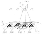
도 2는 본 발명을 구현화하는 형태의 일례에 있어서의 촬상의 모습을 도시하는 개념도이다.
도 3은 본 발명을 구현화하는 형태의 일례에 있어서의 디바이스 칩 C 각각의 위치 관계를 도시하는 평면도이다.
도 4는 본 발명을 구현화하는 형태의 일례에 있어서의 화상 Ps, 기준 화상 Pf, 검사 화상 Pk, 검사 화상 Pk와 기준 화상 Pf의 차분의 이미지를 나타내는 화상 도이다.
도 5는 본 발명을 구현화하는 형태의 일례에 있어서의 화상 Ps, 기준 화상 Pf, 검사 화상 Pk의 각 화소의 휘도값 그리고, 검사 화상 Pk와 기준 화상 Pf의 휘도값의 차분의 이미지를 나타내는 화상도이다.
도 6은 본 발명을 구현화하는 형태의 일례에 있어서의 흐름도이다.
2: 웨이퍼 보유 지지부
3: 촬상부
4: 상대 이동부
5: 칩 레이아웃 등록부
6: 기준 화상 등록부
7: 화상 처리부
1f: 장치 프레임
20: 적재대
30: 경통
31: 조명부
32: 하프 미러
33a, 33b: 대물 렌즈
34: 리볼버 기구
35: 촬상 카메라
41: X축 슬라이더
42: Y축 슬라이더
43: 회전 기구
71: 동적 마스크 처리부
72: 비교 검사부
CN: 제어부
W: 웨이퍼
C: 디바이스 칩
Cn: 완전 칩
Cb: 불완전 칩
F: 촬상 영역(시야)
Ri: 검사 영역
Rn: 비검사 영역
Ps: 검사 화상(처리 전)
Pk: 검사 화상(처리 후)
Pf: 기준 화상
L1: 조명광
L2: 웨이퍼측으로부터 입사한 광(반사광, 산란광)
T: 촬상 루트
Claims (2)
- 웨이퍼 상에 형성된 디바이스 칩의 반복 외관 패턴의 검사 대상 부위를 촬상하고, 기준 화상과 비교하여 당해 디바이스 칩의 검사를 행하는 웨이퍼 외관 검사 장치에 있어서,
상기 웨이퍼를 보유 지지하는 웨이퍼 보유 지지부와,
상기 검사 대상 부위가 포함된 화상을 촬상하는 촬상부와,
상기 웨이퍼 보유 지지부와 상기 촬상부를 상대 이동시키는 상대 이동부와,
상기 웨이퍼의 기준 자세 및 기준 위치에 대한 당해 웨이퍼의 검사 영역 및 비검사 영역의 위치 정보 그리고 디바이스 칩의 배치 정보를 규정하는 칩 레이아웃을 등록하는 칩 레이아웃 등록부와,
상기 기준 화상을 등록하는 기준 화상 등록부와,
상기 촬상부에서 촬상된 상기 화상을 처리하는 화상 처리부를 구비하고,
상기 화상 처리부는,
상기 검사 영역 및 상기 비검사 영역에 걸쳐 형성된 불완전 칩의 상기 검사 대상 부위가 촬상된 상기 화상에 대하여, 당해 화상을 구성하는 화소 중, 상기 비검사 영역에 상당하는 화소의 휘도값을, 당해 화상이 촬상된 상기 웨이퍼 상의 위치 정보와 상기 칩 레이아웃에 기초하여, 상기 기준 화상의 휘도값으로 치환 처리하여 검사 화상을 생성하는, 동적 마스크 처리부와,
상기 동적 마스크 처리부에서 생성된 상기 검사 화상을 상기 기준 화상과 비교하여, 상기 검사 대상 부위에 대하여 검사하는 비교 검사부를 구비한
것을 특징으로 하는 웨이퍼 외관 검사 장치. - 웨이퍼 상에 형성된 디바이스 칩의 반복 외관 패턴의 검사 대상 부위를 촬상하고, 기준 화상과 비교하여 당해 디바이스 칩의 검사를 행하는 웨이퍼 외관 검사 방법에 있어서,
상기 웨이퍼의 기준 자세 및 기준 위치에 대한 당해 웨이퍼의 검사 영역 및 비검사 영역을 규정하는 칩 레이아웃을 미리 등록하는 스텝과,
상기 기준 화상을 미리 등록하는 스텝과,
상기 웨이퍼와 촬상 수단을 상대 이동시키면서 상기 검사 대상 부위가 포함된 화상을 촬상하는 스텝과,
상기 화상을 처리하는 스텝을 갖고,
상기 검사 영역 및 상기 비검사 영역에 걸쳐 형성된 불완전 칩이 촬상된 상기 화상에 대하여, 당해 화상을 구성하는 화소 중, 상기 비검사 영역에 상당하는 화소의 휘도값을, 당해 화상이 촬상된 상기 웨이퍼 상의 위치 정보와 상기 칩 레이아웃에 기초하여, 상기 기준 화상의 휘도값으로 치환 처리하여 검사 화상을 생성하는 스텝과,
상기 검사 화상을 상기 기준 화상과 비교하여, 상기 검사 대상 부위에 대하여 검사하는 스텝을 갖는
것을 특징으로 하는 웨이퍼 외관 검사 방법.
Applications Claiming Priority (3)
| Application Number | Priority Date | Filing Date | Title |
|---|---|---|---|
| JP2019152538A JP7293046B2 (ja) | 2019-08-23 | 2019-08-23 | ウエーハ外観検査装置および方法 |
| JPJP-P-2019-152538 | 2019-08-23 | ||
| PCT/JP2020/022717 WO2021039019A1 (ja) | 2019-08-23 | 2020-06-09 | ウエーハ外観検査装置および方法 |
Publications (2)
| Publication Number | Publication Date |
|---|---|
| KR20220044742A KR20220044742A (ko) | 2022-04-11 |
| KR102764199B1 true KR102764199B1 (ko) | 2025-02-07 |
Family
ID=74678135
Family Applications (1)
| Application Number | Title | Priority Date | Filing Date |
|---|---|---|---|
| KR1020227004449A Active KR102764199B1 (ko) | 2019-08-23 | 2020-06-09 | 웨이퍼 외관 검사 장치 및 방법 |
Country Status (5)
| Country | Link |
|---|---|
| JP (1) | JP7293046B2 (ko) |
| KR (1) | KR102764199B1 (ko) |
| CN (1) | CN114222913B (ko) |
| TW (1) | TWI845721B (ko) |
| WO (1) | WO2021039019A1 (ko) |
Families Citing this family (1)
| Publication number | Priority date | Publication date | Assignee | Title |
|---|---|---|---|---|
| CN118817610A (zh) * | 2024-09-19 | 2024-10-22 | 苏州高视半导体技术有限公司 | 基于晶圆检测系统的晶圆检测方法及其相关产品 |
Citations (5)
| Publication number | Priority date | Publication date | Assignee | Title |
|---|---|---|---|---|
| JP2000346627A (ja) | 1999-06-07 | 2000-12-15 | Toray Eng Co Ltd | 検査装置 |
| JP2007155610A (ja) | 2005-12-07 | 2007-06-21 | Seiko Epson Corp | 外観検査装置および外観検査方法 |
| JP2008244197A (ja) | 2007-03-28 | 2008-10-09 | Hitachi High-Technologies Corp | 検査装置及び検査方法 |
| JP2009097958A (ja) | 2007-10-16 | 2009-05-07 | Tokyo Seimitsu Co Ltd | 欠陥検出装置及び欠陥検出方法 |
| JP2010151655A (ja) | 2008-12-25 | 2010-07-08 | Hitachi High-Technologies Corp | 欠陥検査方法及びその装置 |
Family Cites Families (8)
| Publication number | Priority date | Publication date | Assignee | Title |
|---|---|---|---|---|
| JPH02290036A (ja) | 1989-02-13 | 1990-11-29 | Tokyo Electron Ltd | 半導体ウエハの検査方法 |
| JP2939665B2 (ja) | 1991-03-04 | 1999-08-25 | 東京エレクトロン株式会社 | 半導体ウエハの測定方法 |
| JP2007163259A (ja) * | 2005-12-13 | 2007-06-28 | Dainippon Screen Mfg Co Ltd | 差分比較検査方法および差分比較検査装置 |
| US20100158346A1 (en) * | 2008-12-23 | 2010-06-24 | Wei Fang | Method and system of classifying defects on a wafer |
| JP2009283977A (ja) * | 2009-08-21 | 2009-12-03 | Hitachi High-Technologies Corp | 検査装置及び検査方法 |
| JP5536233B2 (ja) * | 2010-01-21 | 2014-07-02 | ヒューレット−パッカード・インデイゴ・ビー・ブイ | 印刷画像の自動検査 |
| TWI692700B (zh) * | 2017-10-05 | 2020-05-01 | 敖翔科技股份有限公司 | 智慧型的缺陷校正系統與其實施方法 |
| CN108280828B (zh) * | 2018-01-25 | 2020-11-10 | 上海闻泰电子科技有限公司 | 相机装配位置检测方法与装置 |
-
2019
- 2019-08-23 JP JP2019152538A patent/JP7293046B2/ja active Active
-
2020
- 2020-06-09 CN CN202080057392.9A patent/CN114222913B/zh active Active
- 2020-06-09 WO PCT/JP2020/022717 patent/WO2021039019A1/ja not_active Ceased
- 2020-06-09 KR KR1020227004449A patent/KR102764199B1/ko active Active
- 2020-07-14 TW TW109123703A patent/TWI845721B/zh active
Patent Citations (5)
| Publication number | Priority date | Publication date | Assignee | Title |
|---|---|---|---|---|
| JP2000346627A (ja) | 1999-06-07 | 2000-12-15 | Toray Eng Co Ltd | 検査装置 |
| JP2007155610A (ja) | 2005-12-07 | 2007-06-21 | Seiko Epson Corp | 外観検査装置および外観検査方法 |
| JP2008244197A (ja) | 2007-03-28 | 2008-10-09 | Hitachi High-Technologies Corp | 検査装置及び検査方法 |
| JP2009097958A (ja) | 2007-10-16 | 2009-05-07 | Tokyo Seimitsu Co Ltd | 欠陥検出装置及び欠陥検出方法 |
| JP2010151655A (ja) | 2008-12-25 | 2010-07-08 | Hitachi High-Technologies Corp | 欠陥検査方法及びその装置 |
Also Published As
| Publication number | Publication date |
|---|---|
| JP2021032672A (ja) | 2021-03-01 |
| CN114222913B (zh) | 2024-05-24 |
| JP7293046B2 (ja) | 2023-06-19 |
| TW202109022A (zh) | 2021-03-01 |
| CN114222913A (zh) | 2022-03-22 |
| WO2021039019A1 (ja) | 2021-03-04 |
| KR20220044742A (ko) | 2022-04-11 |
| TWI845721B (zh) | 2024-06-21 |
Similar Documents
| Publication | Publication Date | Title |
|---|---|---|
| CN101853797B (zh) | 用于检测晶片的系统和方法 | |
| CN101783306B (zh) | 检测晶片的系统和方法 | |
| TWI881180B (zh) | 外觀檢查裝置及方法 | |
| KR20100071621A (ko) | 반도체 칩 외관 검사 방법 및 그 장치 | |
| KR101802843B1 (ko) | 자동 비전 검사 시스템 | |
| CN112204384B (zh) | 切割芯片检查装置 | |
| JP7368141B2 (ja) | ウエーハ外観検査装置および方法 | |
| KR102764199B1 (ko) | 웨이퍼 외관 검사 장치 및 방법 | |
| JP2021110551A (ja) | 基板エッジ検査装置 | |
| JP2006329714A (ja) | レンズ検査装置 | |
| JP6775389B2 (ja) | 外観検査装置および外観検査方法 | |
| JP4960912B2 (ja) | 自動外観検査装置及び自動外観検査方法 | |
| JPH07209203A (ja) | 外観検査装置および外観検査方法 | |
| JPH11211420A (ja) | 光学式寸法測定方法および装置 | |
| WO2023162523A1 (ja) | ウエーハ検査装置 | |
| CN118451318A (zh) | 晶片外观检查装置 | |
| WO2024042562A1 (ja) | 検査装置及び検査方法 | |
| JP2020046393A (ja) | チップ体の検査装置 |
Legal Events
| Date | Code | Title | Description |
|---|---|---|---|
| PA0105 | International application |
Patent event date: 20220209 Patent event code: PA01051R01D Comment text: International Patent Application |
|
| PG1501 | Laying open of application | ||
| E701 | Decision to grant or registration of patent right | ||
| PE0701 | Decision of registration |
Patent event code: PE07011S01D Comment text: Decision to Grant Registration Patent event date: 20250108 |
|
| GRNT | Written decision to grant | ||
| PR0701 | Registration of establishment |
Comment text: Registration of Establishment Patent event date: 20250203 Patent event code: PR07011E01D |
|
| PR1002 | Payment of registration fee |
Payment date: 20250204 End annual number: 3 Start annual number: 1 |
|
| PG1601 | Publication of registration |