KR20060106005A - 백라이트 유닛 - Google Patents
백라이트 유닛 Download PDFInfo
- Publication number
- KR20060106005A KR20060106005A KR1020050028172A KR20050028172A KR20060106005A KR 20060106005 A KR20060106005 A KR 20060106005A KR 1020050028172 A KR1020050028172 A KR 1020050028172A KR 20050028172 A KR20050028172 A KR 20050028172A KR 20060106005 A KR20060106005 A KR 20060106005A
- Authority
- KR
- South Korea
- Prior art keywords
- light emitting
- electrodes
- common
- common electrode
- emitting lamp
- Prior art date
- Legal status (The legal status is an assumption and is not a legal conclusion. Google has not performed a legal analysis and makes no representation as to the accuracy of the status listed.)
- Granted
Links
Images




Classifications
-
- H—ELECTRICITY
- H01—ELECTRIC ELEMENTS
- H01J—ELECTRIC DISCHARGE TUBES OR DISCHARGE LAMPS
- H01J65/00—Lamps without any electrode inside the vessel; Lamps with at least one main electrode outside the vessel
- H01J65/04—Lamps in which a gas filling is excited to luminesce by an external electromagnetic field or by external corpuscular radiation, e.g. for indicating plasma display panels
- H01J65/042—Lamps in which a gas filling is excited to luminesce by an external electromagnetic field or by external corpuscular radiation, e.g. for indicating plasma display panels by an external electromagnetic field
- H01J65/046—Lamps in which a gas filling is excited to luminesce by an external electromagnetic field or by external corpuscular radiation, e.g. for indicating plasma display panels by an external electromagnetic field the field being produced by using capacitive means around the vessel
-
- B—PERFORMING OPERATIONS; TRANSPORTING
- B43—WRITING OR DRAWING IMPLEMENTS; BUREAU ACCESSORIES
- B43L—ARTICLES FOR WRITING OR DRAWING UPON; WRITING OR DRAWING AIDS; ACCESSORIES FOR WRITING OR DRAWING
- B43L7/00—Straightedges
- B43L7/027—Plural non-adjustable straightedges fixed at right angles
- B43L7/0275—Triangles
-
- G—PHYSICS
- G01—MEASURING; TESTING
- G01B—MEASURING LENGTH, THICKNESS OR SIMILAR LINEAR DIMENSIONS; MEASURING ANGLES; MEASURING AREAS; MEASURING IRREGULARITIES OF SURFACES OR CONTOURS
- G01B3/00—Measuring instruments characterised by the use of mechanical techniques
- G01B3/002—Details
- G01B3/004—Scales; Graduations
-
- G—PHYSICS
- G02—OPTICS
- G02F—OPTICAL DEVICES OR ARRANGEMENTS FOR THE CONTROL OF LIGHT BY MODIFICATION OF THE OPTICAL PROPERTIES OF THE MEDIA OF THE ELEMENTS INVOLVED THEREIN; NON-LINEAR OPTICS; FREQUENCY-CHANGING OF LIGHT; OPTICAL LOGIC ELEMENTS; OPTICAL ANALOGUE/DIGITAL CONVERTERS
- G02F1/00—Devices or arrangements for the control of the intensity, colour, phase, polarisation or direction of light arriving from an independent light source, e.g. switching, gating or modulating; Non-linear optics
- G02F1/01—Devices or arrangements for the control of the intensity, colour, phase, polarisation or direction of light arriving from an independent light source, e.g. switching, gating or modulating; Non-linear optics for the control of the intensity, phase, polarisation or colour
- G02F1/13—Devices or arrangements for the control of the intensity, colour, phase, polarisation or direction of light arriving from an independent light source, e.g. switching, gating or modulating; Non-linear optics for the control of the intensity, phase, polarisation or colour based on liquid crystals, e.g. single liquid crystal display cells
- G02F1/133—Constructional arrangements; Operation of liquid crystal cells; Circuit arrangements
- G02F1/1333—Constructional arrangements; Manufacturing methods
- G02F1/1335—Structural association of cells with optical devices, e.g. polarisers or reflectors
- G02F1/1336—Illuminating devices
- G02F1/133602—Direct backlight
- G02F1/133604—Direct backlight with lamps
-
- H—ELECTRICITY
- H01—ELECTRIC ELEMENTS
- H01J—ELECTRIC DISCHARGE TUBES OR DISCHARGE LAMPS
- H01J61/00—Gas-discharge or vapour-discharge lamps
- H01J61/02—Details
- H01J61/30—Vessels; Containers
- H01J61/32—Special longitudinal shape, e.g. for advertising purposes
- H01J61/325—U-shaped lamps
-
- G—PHYSICS
- G02—OPTICS
- G02F—OPTICAL DEVICES OR ARRANGEMENTS FOR THE CONTROL OF LIGHT BY MODIFICATION OF THE OPTICAL PROPERTIES OF THE MEDIA OF THE ELEMENTS INVOLVED THEREIN; NON-LINEAR OPTICS; FREQUENCY-CHANGING OF LIGHT; OPTICAL LOGIC ELEMENTS; OPTICAL ANALOGUE/DIGITAL CONVERTERS
- G02F1/00—Devices or arrangements for the control of the intensity, colour, phase, polarisation or direction of light arriving from an independent light source, e.g. switching, gating or modulating; Non-linear optics
- G02F1/01—Devices or arrangements for the control of the intensity, colour, phase, polarisation or direction of light arriving from an independent light source, e.g. switching, gating or modulating; Non-linear optics for the control of the intensity, phase, polarisation or colour
- G02F1/13—Devices or arrangements for the control of the intensity, colour, phase, polarisation or direction of light arriving from an independent light source, e.g. switching, gating or modulating; Non-linear optics for the control of the intensity, phase, polarisation or colour based on liquid crystals, e.g. single liquid crystal display cells
- G02F1/133—Constructional arrangements; Operation of liquid crystal cells; Circuit arrangements
- G02F1/1333—Constructional arrangements; Manufacturing methods
- G02F1/1335—Structural association of cells with optical devices, e.g. polarisers or reflectors
- G02F1/1336—Illuminating devices
- G02F1/133602—Direct backlight
- G02F1/133612—Electrical details
-
- G—PHYSICS
- G09—EDUCATION; CRYPTOGRAPHY; DISPLAY; ADVERTISING; SEALS
- G09G—ARRANGEMENTS OR CIRCUITS FOR CONTROL OF INDICATING DEVICES USING STATIC MEANS TO PRESENT VARIABLE INFORMATION
- G09G2330/00—Aspects of power supply; Aspects of display protection and defect management
- G09G2330/06—Handling electromagnetic interferences [EMI], covering emitted as well as received electromagnetic radiation
-
- G—PHYSICS
- G09—EDUCATION; CRYPTOGRAPHY; DISPLAY; ADVERTISING; SEALS
- G09G—ARRANGEMENTS OR CIRCUITS FOR CONTROL OF INDICATING DEVICES USING STATIC MEANS TO PRESENT VARIABLE INFORMATION
- G09G3/00—Control arrangements or circuits, of interest only in connection with visual indicators other than cathode-ray tubes
- G09G3/20—Control arrangements or circuits, of interest only in connection with visual indicators other than cathode-ray tubes for presentation of an assembly of a number of characters, e.g. a page, by composing the assembly by combination of individual elements arranged in a matrix no fixed position being assigned to or needed to be assigned to the individual characters or partial characters
- G09G3/34—Control arrangements or circuits, of interest only in connection with visual indicators other than cathode-ray tubes for presentation of an assembly of a number of characters, e.g. a page, by composing the assembly by combination of individual elements arranged in a matrix no fixed position being assigned to or needed to be assigned to the individual characters or partial characters by control of light from an independent source
- G09G3/3406—Control of illumination source
Landscapes
- Physics & Mathematics (AREA)
- Electromagnetism (AREA)
- Engineering & Computer Science (AREA)
- Plasma & Fusion (AREA)
- Nonlinear Science (AREA)
- General Physics & Mathematics (AREA)
- Mathematical Physics (AREA)
- Chemical & Material Sciences (AREA)
- Crystallography & Structural Chemistry (AREA)
- Optics & Photonics (AREA)
- Planar Illumination Modules (AREA)
- Liquid Crystal (AREA)
Abstract
Description
Claims (18)
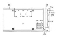
- 외곽 케이스상에 관(tube)의 양단이 동일 방향에 배열되며, 관(tube)의 양단에 제 1, 제 2 전극이 구성된 복수개의 발광램프들과;상기 발광램프의 상기 제 1, 제 2 전극과 접속된 제 1, 제 2 전원선들과;상기 발광램프의 양단에 인접한 상기 외곽 케이스의 측면에 배치된 공통전극 PCB와;상기 제 1, 제 2 전원선들과 접속되도록 상기 공통전극 PCB상에 이격 형성된 제 1, 제 2 공통전극과;상기 외곽 케이스의 배면에 상기 제 1, 제 2 공통전극에 전원을 인가시키기 위해 배치된 인버터를 포함하여 구성됨을 특징으로 하는 백라이트 유닛.
- 제 1 항에 있어서,상기 발광램프는 'U'자형으로 구성되어 있음을 특징으로 하는 백라이트 유닛.
- 제 1 항에 있어서,상기 공통전극 PCB에는 상기 발광램프 양단에 대응되는 부분에 복수개의 제 1, 제 2 접속점들이 있고, 상기 제 1, 제 2 접속점을 통해서 상기 제 1, 제 2 전원선과 상기 제 1, 제 2 공통전극이 각각 연결됨을 특징으로 하는 백라이트 유닛.
- 제 1 항에 있어서,상기 제 1, 제 2 전원선들은 상기 발광램프를 테이핑하기 전에 양단의 상기 제 1, 제 2 전극과 제 1, 제 2 전원선들을 각각 도전성을 갖는 호일로 감아서 접속시킴을 특징으로 하는 백라이트 유닛.
- 제 1 항에 있어서,상기 제 1, 제 2 공통전극의 각 일끝단에는 제 1, 제 2 공통전압 입력선이 상기 외곽 케이스 배면으로 돌출되어 있음을 특징으로 하는 백라이트 유닛.
- 제 3 항에 있어서,상기 제 1, 제 2 전원선은 상기 제 1, 제 2 접속점에 각각 납땝하여 접속됨을 특징으로 하는 백라이트 유닛.
- 제 1 항에 있어서,상기 제 1, 제 2 공통전극은 서로 이격되도록 굴곡지게 형성되어 있으며, 도전성 물질로 패턴 형성되어 있음을 특징으로 하는 백라이트 유닛.
- 제 7 항에 있어서,상기 제 1, 제 2 공통전극의 사이에 슬릿(Slit)이 형성되는 것을 포함함을 특징으로 하는 백라이트 유닛.
- 제 1 항에 있어서,상기 제 1, 제 2 공통전극은 각 표면에 실크(silk) 처리가 되어 있는 것을 더 포함함을 특징으로 하는 백라이트 유닛.
- 제 9 항에 있어서,상기 실크(silk) 처리는 상기 제 1, 제 2 공통전극의 각 표면에 비도전성 흰색 물감이 발라져서 이루어짐을 특징으로 하는 백라이트 유닛.
- 제 1 항에 있어서,상기 발광램프는 관의 양단 외부에 전극이 형성된 외부전극 발광램프로 구성함을 특징으로 하는 백라이트 유닛.
- 제 1 항에 있어서,상기 발광램프는 관의 양단 내부에 제 1, 제 2 전극이 형성된 냉음극관 램프로 구성하고, 상기 제 1, 제 2 전원선 대신에 상기 제 1, 제 2 전극에 연결된 제 1, 제 2 전원인입선을 사용하는 것을 더 포함함을 특징으로 하는 백라이트 유닛.
- 외곽 케이스상에 관의 양단이 동일 방향에 배열되고, 좌우측에 대칭적으로 배열되며, 좌측에 배열된 관(tube)의 양단 외부에 제 1, 제 2 외부전극이 구성되고, 우측에 배열된 관(tube)의 양단 외부에 제 3, 제 4 외부전극이 구성된 복수개의 발광램프(EEFL)들과;상기 발광램프의 상기 제 1 내지 제 4 외부전극과 각각 접속된 제 1 내지 제 4 전원선들과;상기 발광램프의 양단에 인접한 상기 외곽 케이스의 좌우측면에 각각 배치된 제 1, 제 2 공통전극 PCB와;상기 제 1, 제 2 전원선들과 접속되도록 상기 제 1 공통전극 PCB상에 이격 형성된 제 1, 제 2 공통전극과;상기 제 3, 제 4 전원선들과 접속되도록 상기 제 2 공통전극 PCB상에 이격 형성된 제 3, 제 4 공통전극과;상기 외곽 케이스의 배면에 상기 제 1, 제 2 공통전극 및 제 3, 제 4 공통전극에 전원을 인가시키기 위해 좌우측에 각각 배치된 제 1, 제 2 인버터를 포함하여 구성됨을 특징으로 하는 백라이트 유닛.
- 제 13 항에 있어서,상기 제 1 공통전극 PCB에는 상기 발광램프 양단에 대응되는 부분에 복수개의 제 1, 제 2 접속점들이 있고, 상기 제 1, 제 2 접속점을 통해서 상기 제 1, 제 2 전원선과 상기 제 1, 제 2 공통전극이 각각 연결되고,상기 제 2 공통전극 PCB에는 상기 발광램프 양단에 대응되는 부분에 복수개 의 제 3, 제 4 접속점들이 있고, 상기 제 3, 제 4 접속점을 통해서 상기 제 3, 제 4 전원선과 상기 제 3, 제 4 공통전극이 각각 연결됨을 특징으로 하는 백라이트 유닛.
- 제 13 항에 있어서,상기 제 1, 제 2 공통전극의 사이 및 상기 제 3, 제 4 공통전극의 사이에 슬릿(Slit)이 형성된 것을 특징으로 하는 백라이트 유닛.
- 제 13 항에 있어서,상기 제 1 내지 제 4 공통전극은 각 표면에 실크(silk) 처리가 되어 있는 것을 더 포함함을 특징으로 하는 백라이트 유닛.
- 제 13 항에 있어서,상기 발광램프는 관의 양단 내부에 내부전극이 형성된 냉음극관 램프로 구성하고, 상기 제 1 내지 제 4 전원선 대신에 제 1 내지 제 4 전원인입선을 사용하는 것을 더 포함함을 특징으로 하는 백라이트 유닛.
- 전체 화면이 N분할되고, 각 분할 영역에 관(tube)의 양단이 동일 방향에 배열되고, 각 관의 양단에 제 1, 제 2 전극이 구성되도록 외곽 케이스 상에 배열된 복수개의 발광램프들과;상기 각 분할 영역의 일측면에 일대일 대응되도록 구성된 N개의 공통전극 PCB와;상기 각 N개의 공통전극 PCB상에 상기 발광램프의 제 1, 제 2 전극과 제 1, 제 2 접속점을 통해 접속되도록 일정간격 이격 형성된 제 1, 제 2 공통전극과;상기 발광램프에 전원을 인가시키기 위해서 외곽 케이스의 배면 양측 중간부분에 배치된 제 1, 제 2 인버터를 포함함을 특징으로 하는 백라이트 유닛.
Priority Applications (2)
| Application Number | Priority Date | Filing Date | Title |
|---|---|---|---|
| KR1020050028172A KR101096691B1 (ko) | 2005-04-04 | 2005-04-04 | 백라이트 유닛 |
| US11/395,163 US7364316B2 (en) | 2005-04-04 | 2006-04-03 | Backlight unit |
Applications Claiming Priority (1)
| Application Number | Priority Date | Filing Date | Title |
|---|---|---|---|
| KR1020050028172A KR101096691B1 (ko) | 2005-04-04 | 2005-04-04 | 백라이트 유닛 |
Publications (2)
| Publication Number | Publication Date |
|---|---|
| KR20060106005A true KR20060106005A (ko) | 2006-10-12 |
| KR101096691B1 KR101096691B1 (ko) | 2011-12-22 |
Family
ID=37070173
Family Applications (1)
| Application Number | Title | Priority Date | Filing Date |
|---|---|---|---|
| KR1020050028172A Expired - Fee Related KR101096691B1 (ko) | 2005-04-04 | 2005-04-04 | 백라이트 유닛 |
Country Status (2)
| Country | Link |
|---|---|
| US (1) | US7364316B2 (ko) |
| KR (1) | KR101096691B1 (ko) |
Cited By (1)
| Publication number | Priority date | Publication date | Assignee | Title |
|---|---|---|---|---|
| KR100925546B1 (ko) * | 2006-12-11 | 2009-11-05 | 엘지디스플레이 주식회사 | 백라이트 유닛 및 이를 포함하는 액정표시장치모듈 |
Families Citing this family (2)
| Publication number | Priority date | Publication date | Assignee | Title |
|---|---|---|---|---|
| US7878698B2 (en) * | 2005-09-28 | 2011-02-01 | Sharp Kabushiki Kaisha | Backlight unit and liquid crystal display device |
| WO2010126226A2 (en) * | 2009-04-27 | 2010-11-04 | Lg Electronics Inc. | Back light unit and display device using the same |
Family Cites Families (10)
| Publication number | Priority date | Publication date | Assignee | Title |
|---|---|---|---|---|
| US20030142487A1 (en) * | 2002-01-29 | 2003-07-31 | Chi Mei Optoelectronics Corp. | Liquid crystal display device and backlight module thereof |
| JP4371675B2 (ja) | 2003-03-12 | 2009-11-25 | Necライティング株式会社 | 面光源、バックライト装置及び液晶ディスプレイパネル |
| TW200424475A (en) * | 2003-05-07 | 2004-11-16 | Au Optronics Corp | Back light module |
| TWI232986B (en) * | 2003-05-23 | 2005-05-21 | Au Optronics Corp | Backlight source |
| KR20060047404A (ko) * | 2004-04-23 | 2006-05-18 | 마츠시타 덴끼 산교 가부시키가이샤 | 구부러진 형광램프를 포함하는 백라이트 유닛,및 이백라이트 유닛을 포함하는 액정 디스플레이 장치 |
| KR101016289B1 (ko) * | 2004-06-30 | 2011-02-22 | 엘지디스플레이 주식회사 | 백라이트 유닛 |
| KR100760941B1 (ko) * | 2004-09-23 | 2007-09-21 | 엘지.필립스 엘시디 주식회사 | 백라이트 유닛 및 그의 구동 방법 |
| TWI265351B (en) * | 2004-12-06 | 2006-11-01 | Chi Mei Optoelectronics Corp | Backlight module |
| KR101137868B1 (ko) * | 2005-06-30 | 2012-04-23 | 엘지디스플레이 주식회사 | 백라이트 유닛 및 그의 구동방법 |
| KR101183447B1 (ko) * | 2005-06-30 | 2012-09-17 | 엘지디스플레이 주식회사 | 액정표시장치용 반사시트 및 이를 이용한백라이트어셈블리와 액정표시장치모듈 |
-
2005
- 2005-04-04 KR KR1020050028172A patent/KR101096691B1/ko not_active Expired - Fee Related
-
2006
- 2006-04-03 US US11/395,163 patent/US7364316B2/en not_active Expired - Fee Related
Cited By (1)
| Publication number | Priority date | Publication date | Assignee | Title |
|---|---|---|---|---|
| KR100925546B1 (ko) * | 2006-12-11 | 2009-11-05 | 엘지디스플레이 주식회사 | 백라이트 유닛 및 이를 포함하는 액정표시장치모듈 |
Also Published As
| Publication number | Publication date |
|---|---|
| US20060221639A1 (en) | 2006-10-05 |
| KR101096691B1 (ko) | 2011-12-22 |
| US7364316B2 (en) | 2008-04-29 |
Similar Documents
| Publication | Publication Date | Title |
|---|---|---|
| KR100493386B1 (ko) | 백 라이트 유닛 | |
| KR101074391B1 (ko) | 백라이트 유닛 | |
| KR100623845B1 (ko) | 백라이트 어셈블리 및 이를 구비한 액정표시장치 | |
| KR100525440B1 (ko) | 백 라이트 유닛 | |
| KR20080053880A (ko) | 백라이트 유닛 및 이를 포함하는 액정표시장치모듈 | |
| KR100641005B1 (ko) | 백라이트 유닛 | |
| US7999784B2 (en) | Backlight unit of liquid crystal display device and method for driving the same | |
| KR101068385B1 (ko) | 액정표시장치 백라이트 어셈블리 및 전극판 구조 | |
| KR101137868B1 (ko) | 백라이트 유닛 및 그의 구동방법 | |
| KR101096691B1 (ko) | 백라이트 유닛 | |
| KR100587371B1 (ko) | 백라이트 유닛 및 그의 구동방법 | |
| KR101157951B1 (ko) | 백라이트 유닛 | |
| KR100929206B1 (ko) | 액정표시장치모듈 | |
| KR100418929B1 (ko) | 액정표시장치의 백라이트 | |
| KR101318223B1 (ko) | 액정표시장치모듈 | |
| KR100418930B1 (ko) | 액정표시장치의 백라이트 | |
| KR100480829B1 (ko) | 백라이트 유닛의 구동방법 | |
| KR101055205B1 (ko) | 형광램프 및 이를 구비한 백라이트 유닛 | |
| KR101009681B1 (ko) | 백라이트 유닛 및 이를 이용한 액정표시모듈 | |
| KR20080073572A (ko) | 액정표시장치 및 백라이트 구조 | |
| KR20050067935A (ko) | 백라이트 유닛 | |
| KR20060134349A (ko) | 백라이트 유닛 | |
| KR20080047813A (ko) | 백라이트 어셈블리 및 이를 이용한 액정 표시 장치 |
Legal Events
| Date | Code | Title | Description |
|---|---|---|---|
| PA0109 | Patent application |
St.27 status event code: A-0-1-A10-A12-nap-PA0109 |
|
| PG1501 | Laying open of application |
St.27 status event code: A-1-1-Q10-Q12-nap-PG1501 |
|
| PN2301 | Change of applicant |
St.27 status event code: A-3-3-R10-R13-asn-PN2301 St.27 status event code: A-3-3-R10-R11-asn-PN2301 |
|
| A201 | Request for examination | ||
| PA0201 | Request for examination |
St.27 status event code: A-1-2-D10-D11-exm-PA0201 |
|
| R18-X000 | Changes to party contact information recorded |
St.27 status event code: A-3-3-R10-R18-oth-X000 |
|
| E902 | Notification of reason for refusal | ||
| PE0902 | Notice of grounds for rejection |
St.27 status event code: A-1-2-D10-D21-exm-PE0902 |
|
| P11-X000 | Amendment of application requested |
St.27 status event code: A-2-2-P10-P11-nap-X000 |
|
| P13-X000 | Application amended |
St.27 status event code: A-2-2-P10-P13-nap-X000 |
|
| R18-X000 | Changes to party contact information recorded |
St.27 status event code: A-3-3-R10-R18-oth-X000 |
|
| E701 | Decision to grant or registration of patent right | ||
| PE0701 | Decision of registration |
St.27 status event code: A-1-2-D10-D22-exm-PE0701 |
|
| GRNT | Written decision to grant | ||
| PR0701 | Registration of establishment |
St.27 status event code: A-2-4-F10-F11-exm-PR0701 |
|
| PR1002 | Payment of registration fee |
St.27 status event code: A-2-2-U10-U11-oth-PR1002 Fee payment year number: 1 |
|
| PG1601 | Publication of registration |
St.27 status event code: A-4-4-Q10-Q13-nap-PG1601 |
|
| R18-X000 | Changes to party contact information recorded |
St.27 status event code: A-5-5-R10-R18-oth-X000 |
|
| FPAY | Annual fee payment |
Payment date: 20141124 Year of fee payment: 4 |
|
| PR1001 | Payment of annual fee |
St.27 status event code: A-4-4-U10-U11-oth-PR1001 Fee payment year number: 4 |
|
| PR1001 | Payment of annual fee |
St.27 status event code: A-4-4-U10-U11-oth-PR1001 Fee payment year number: 5 |
|
| FPAY | Annual fee payment |
Payment date: 20161118 Year of fee payment: 6 |
|
| PR1001 | Payment of annual fee |
St.27 status event code: A-4-4-U10-U11-oth-PR1001 Fee payment year number: 6 |
|
| FPAY | Annual fee payment |
Payment date: 20171116 Year of fee payment: 7 |
|
| PR1001 | Payment of annual fee |
St.27 status event code: A-4-4-U10-U11-oth-PR1001 Fee payment year number: 7 |
|
| FPAY | Annual fee payment |
Payment date: 20181114 Year of fee payment: 8 |
|
| PR1001 | Payment of annual fee |
St.27 status event code: A-4-4-U10-U11-oth-PR1001 Fee payment year number: 8 |
|
| PC1903 | Unpaid annual fee |
St.27 status event code: A-4-4-U10-U13-oth-PC1903 Not in force date: 20191215 Payment event data comment text: Termination Category : DEFAULT_OF_REGISTRATION_FEE |
|
| PC1903 | Unpaid annual fee |
St.27 status event code: N-4-6-H10-H13-oth-PC1903 Ip right cessation event data comment text: Termination Category : DEFAULT_OF_REGISTRATION_FEE Not in force date: 20191215 |